 English
 Arabic
 Chinese (Simplified)
 Dutch
Dutch French
 German
 Italian
 Portuguese
 Russian
 Spanish

Ball Grid Array (BGA) package technology places small solder spheres beneath a component. You build modern bga assembly layouts by placing parts onto a pcb surface. Regular cameras cannot check hidden solder joints under the component package. The solid bga body blocks your view entirely. You cannot find hidden pcb assembly defects using just your eyes.
Advanced bga x-ray inspection relies on differences in material thickness. An x-ray beam passes through the pcb. Thick solder absorbs x-ray energy, while lighter pcb layers let the radiation pass. You inspect every hidden bga joint without damaging the parts. This x-ray method checks joint strength and spots problems quickly. Professional BGA Assembly Services make sure products work well. Careful bga pcb assembly testing promises lasting dependability for critical electronic devices.
Key Takeaways
- BGA packages cover their solder connections under the chip, which makes normal visual checking impossible.
- X-ray testing looks inside dark parts to find hidden problems like gaps and short circuits fast.
- 3D X-ray machines check detailed circuit board layers to measure solder joint strength correctly.
- Official rules say that total empty spaces in the solder must remain below 25 percent to keep the connection reliable.
What is BGA Assembly and Why Visual Inspection Fails
Fundamentals of BGA Assembly Services
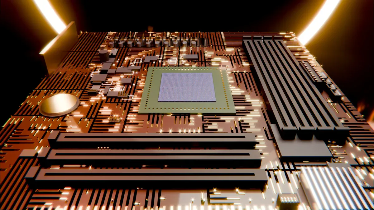
Modern bga assembly services rely on tightly packed part designs. A bga component features small solder balls arranged directly under its body. First, you place this component right onto a surface mount pcb. Next, heat melts these solder spheres onto copper pads during reflow soldering. Engineers often pick bga assembly services to build smaller, tighter pcb designs.
However, this design hides every single solder connection beneath the main chip. Consequently, you cannot see any solder joints after securing the part to a pcb. High-quality precision bga assembly demands total control over every step. Reliable professional bga pcb assembly needs exact heat settings throughout the build process. Furthermore, advanced bga pcb assembly helps prevent broken or cracked solder joints. You can trust bga assembly services to deliver fully working circuit boards. Standard bga assembly produces fantastic results for complex devices. Ultimately, robust bga assembly ensures your electronics last for a very long time.
Limitations of Optical Inspection in SMT
Basic optical tools depend on standard lights and external surface cameras. These cameras only scan the outer surfaces of your pcb. Unfortunately, component bodies block the camera view of hidden parts completely. Because of this, cameras often miss serious pcb assembly defects tucked away underneath the chip.
Because most solder joints are hidden beneath the package, optical inspection alone cannot fully evaluate the integrity of every connection. AOI systems are also limited by line-of-sight visibility and cannot directly inspect hidden solder joints underneath BGA packages.
Standard optical tools frequently overlook hidden faults inside the board. Therefore, you should use x-ray systems to find invisible assembly defects. Powerful x-ray radiation travels through parts to expose deep internal structures. Simple visual bga inspection just cannot check the actual solder strength on a pcb. The table below lists three common hidden issues:
| Defect Type | Reason Optical Inspection Cannot Detect/Evaluate |
|---|---|
| Open Solder Joints | They may not be visible externally as they are hidden beneath the BGA package, requiring inspection of the internal connection integrity. |
| Solder Voids (Internal) | These are gas-filled cavities trapped within the solder joint, requiring visualization of the joint’s internal structure. |
| Solder Bridging (Hidden) | When bridging occurs between hidden joints beneath the package, it is not within the line-of-sight of optical systems. |
Strong x-ray beams easily travel right through the component package. Then, high-definition x-ray images clearly reveal differences in solder density. Advanced precision x-ray equipment quickly locates tiny solder voids hidden inside your pcb. Modern x-ray scanning keeps production quality high for every pcb project. Ultimately, you can catch and remove hidden assembly defects right away.
Mechanics of BGA X-Ray Inspection for Circuit Boards
2D and 3D X-Ray Inspection Capabilities
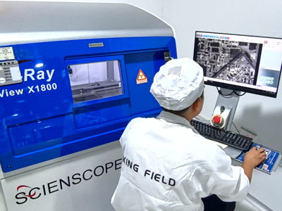
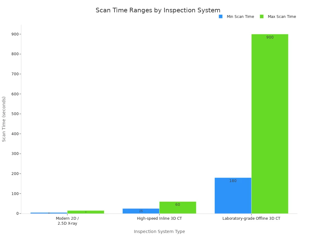
You can evaluate complex pcb designs using modern x-ray inspection capabilities. Standard 2D equipment captures quick top-down images of your board layout. This flat image helps you locate hidden bridge connections fast. However, complex builds require high-resolution pcb x-ray inspection to evaluate depth. High-speed inline 3D systems scan a pcb in 25–60 seconds. Modern pcb x-ray inspection services rely on these distinct x-ray inspection capabilities to maximize manufacturing throughput.
The 2D X-ray inspection system has the ability to detect detail down to 0.5 µm, which represents the finest resolvable feature size.
You need 3D tomography to verify solder joint integrity across layered components. Advanced 3D bga x-ray inspection creates cross-sectional slice views of every joint. This detailed analysis of hidden solder joints reveals severe defects beneath the bga package. You can quickly see how different technologies detect specific bga defects below:
| X-ray Technology | Detection Capability for Head-in-Pillow Defects |
|---|---|
| 2D X-Ray | Limited – provides flat view, lacks depth, hard to detect defects |
| 2.5D X-Ray | Moderate – tilted perspective offers better visibility |
| 3D X-Ray (CT) | Superior – fully visualizes the defect, shows separation between solder layers |
Different equipment types offer varying scan speeds for your bga pcb project. High-volume bga assembly lines use fast systems to keep production moving efficiently.
Material Density Contrast in Solder Testing
Material thickness controls how much x-ray energy moves through your circuit board. Heavy solder metals block energy to form dark spots on the screen image. Light board materials let rays pass through easily, making pale areas. This clear difference helps high-resolution pcb x-ray inspection systems locate hidden air bubbles. Today’s bga x-ray checking tests exact thickness variations across hidden connections.
You can check small bga solder balls down to 0.3 mm with modern x-ray testing tools. This method checks inner empty spots to protect overall board quality. Rules like IPC-7095D and IPC-A-610 say an inner void area below 25% for each ball is fine. Any empty space over 25% makes a fault that hurts device strength. Expert pcb x-ray inspection services watch these limits to ensure top product standard.
Good bga checking boosts the long-term working safety of important electronic tools. Standard bga components need strict testing to confirm hidden wire links. You can trust targeted bga x-ray inspection to find hidden physical flaws before shipping. Leading pcb x-ray inspection services use these smart x-ray inspection capabilities to check total board strength. Exact thickness readings guard final pcb performance in tough working conditions, which raises overall product trust.
How KING FIELD Guarantees BGA Solder Joint Reliability
Common Hidden Defects Identified by X-Ray
Catching invisible circuit board problems early helps keep your electronic devices working well. Dense component chips often cover big issues under heavy metal solder connections. Modern scanners create clear pictures to show hidden assembly flaws without breaking your parts. Professional pcb x-ray inspection services spot these five major internal flaws:
- Solder Voids: Trapped gas creates air bubbles that weaken connections and lower long-term strength.
- Solder Bridging: Extra liquid metal spills into neighboring spaces, causing accidental power shorts.
- Electrical Shorts: Melted metal traces incorrectly join different signal paths during heat processing.
- Open Circuits: Broken contact paths leave gaps between component spheres and copper board spots.
- Head-in-Pillow (HiP): Bent chips touch paste without melting together, which ruins connection strength.
IPC-A-610 is the inspection standard while J-STD-001 defines process controls. High-reliability electronics require strict adherence to both specifications during manufacturing.
Setting up scanner machines correctly helps technicians find tiny internal cracks inside each chip link. Key settings for finding small voids include:
- Tube voltage stability
- Focal spot size (<1 µm)
- Detector pixel pitch
- Geometric magnification (up to 2000×)
- Thermal stability of the sealed-tube X-ray source
Tough testing rules help guarantee strong product quality across many different market uses:
| Standard | Application | BGA Voiding Limit | Context |
|---|---|---|---|
| IPC-A-610 Class 3 | Medical electronics | ≤10% (Target Condition) | Required for long-term reliability |
| IPC-A-610 Class 1 | General consumer electronics | ≤25% | Non-critical applications |
Through careful testing steps, pcb x-ray inspection services find hidden flaws before boards ship out.
Advanced SMT Quality Control at KING FIELD
KING FIELD offers more than twenty years of factory experience for every client project. You get help from pcb x-ray inspection experts who ensure defect-free circuit boards. Our technical workers carefully check connection strength across all bga pcb assembly jobs. We run fine-tuned bga x-ray inspection tools to shield high-reliability electronics from breaking later.
Our pairs automated surface mounting tools with direct x-ray picture checks. We scan every board level to protect product quality for mission-critical electronics. Modern bga x-ray inspection finds deep hidden bubbles, bridges, and loose links under thick covers. You skip expensive fix costs because early defect finds guard total product work.
BGA X-Ray Inspection Process
Material Density Contrast Scan
Defect Detection & Void Analysis
Quality Verification & Reporting
Our strong factory steps make full bga testing necessary for high-reliability electronics. KING FIELD adjusts bga assembly services to fit tough industrial, medical, and car uses. Our technical team tweaks oven heating levels to stop part bending before damage happens. Careful bga assembly methods protect thin wire paths on crowded board surfaces.
We provide adaptable factory orders while keeping steady connection strength for customers worldwide. Industrial-grade pcb x-ray inspection services remove hidden building risks completely. You can depend on our bga assembly work to pass tough international quality rules. KING FIELD keeps improving every bga pcb assembly path using steady quality checks. Our big focus on careful testing brings high manufacturing success to your builds.
You can keep your circuit boards safe by using bga x-ray inspection. Modern bga components block your view of hidden bga solder joints beneath the bga package. Powerful x-ray beams spot unseen assembly flaws with ease. Advanced bga x-ray inspection guards the strength of every bga solder joint on your board.
Combining accurate bga assembly techniques with smart 2D/3D x-ray testing improves overall build quality. These helpful pcb x-ray inspection services find hidden defects before your products ship out. This complete approach lets you create high-reliability electronics while keeping total pcb yield very high.
KING FIELD provides excellent circuit board manufacturing for customers around the world. We carefully refine your bga assembly process on every single bga pcb. You achieve outstanding results for your high-reliability electronics projects. Our thorough pcb x-ray inspection services promise long-lasting product reliability. You can trust KING FIELD for complete bga pcb performance.
FAQ
What makes a bga component different from other pcb parts?
A bga package has tiny solder spheres underneath it instead of side pins. You place this bga component right on top of a pcb surface. This clever design helps save valuable space on your pcb. However, the chip body hides all the solder joints during assembly.
Why do you need x-ray testing for bga assembly?
Normal cameras cannot see underneath the dark chip packages. An x-ray machine sends safe rays through the board to check hidden links. The x-ray beam shows hidden density changes right away. You can easily find big problems like voids or shorts inside your bga board.
What specific defects can an x-ray scanner detect?
An x-ray tool spots solder voids, bridging, and broken paths. The machine catches Head-in-Pillow issues very fast. Scanning your pcb stops future product failures. This careful check protects total product reliability across every making batch.
How does x-ray inspection improve pcb reliability?
Detailed x-ray testing finds tiny solder flaws before shipping. Finding problems early keeps weak pcb builds out of final assembly. You check total joint strength on every bga layout. Smart testing boosts long-term device reliability for your hardest jobs.
What voiding limit applies to bga solder joints on a pcb?
Common rules like IPC-A-610 need a bga void space under 25%. Modern x-ray tools measure inner air bubbles correctly. You keep top pcb quality across every single project. Checking every bga part protects your finished pcb assembly.