 English
 Arabic
 Chinese (Simplified)
 Dutch
Dutch French
 German
 Italian
 Portuguese
 Russian
 Spanish

You need professional PCB layout services to change your circuit blueprints into real board layouts. Skilled PCB design services turn simple electronic ideas into dependable hardware. Expert engineering teams finish your PCB layout design using precise wire routing and heat control.
You will receive important technical files for smooth PCB production:
- Gerber and ODB++ layout files
- Accurate NC drill data and building drawings
- Combined 3D CAD models for outer case fitting
KING FIELD brings more than twenty years of work experience to your custom PCB design projects. Our team provides full design, PCB making, and total assembly services to ensure your product succeeds.
Key Takeaways
- Expert PCB layout services turn simple circuit diagrams into sturdy, real-world circuit boards.
- Full design sets give correct factory files to stop expensive making errors.
- Good component placement boosts air movement and shields sensitive electronics from strong heat.
- Checking your design early speeds up product making and saves money on fixing boards.
Scope and Process of PCB Layout Services

Expert pcb layout services turn simple circuit diagrams into real circuit board designs. Smart engineering teams lead your custom pcb design through organized hardware steps. They give you the best design settings for making test boards and big factory runs.
Schematic Capture and Component Placement
The design process connects basic circuit ideas with real pcb board parts. You must change drawing symbols into correct physical component footprints. Engineers use clear step-by-step actions to ensure perfect netlist file transfers:
- List basic circuit needs like working voltage, current levels, and signal types.
- Pick parts using proper power ratings and matching physical shapes.
- Make the main schematic drawing with normal component symbols.
- Add exact footprint patterns to every single schematic part.
- Run a basic Electrical Rule Check to fix simple wiring mistakes.
- Create a clean netlist file that moves data into the pcb software.
After exporting the netlist, careful component placement starts. Smart component placement cuts down electrical noise and controls heat across board areas. You must group working parts together to make signal paths much easier to draw. Designers also place parts by their electrical jobs, like power areas or sensor parts, to make wiring simple. Good component placement keeps cool chips away from hot power parts. Putting main plugs near board edges makes connecting cables much easier. Wise component placement stops overlapping lines, lowers unwanted power loss, and helps routing. Best component placement improves air movement and makes checking boards simple. Careful part placement guarantees good physical space inside product cases.
Layer Stackup Design, Routing, and DFM
Choosing the right layer stackup directly changes total board performance. Multilayer pcb stackups give you solid reference ground planes. Picking good board materials like standard FR-4 or high-frequency Rogers keeps signal speeds steady. An 8-layer pcb layout design provides great signal quality and strong power flow.
Next, engineers draw wire lines across signal layers using strict design rules. High-speed routing needs accurate line width math to hit matching power targets.
| Aspect | Standard Trace Routing | Impedance-Controlled Trace Routing |
|---|---|---|
| Core Objective | Basic trace connectivity | Match target impedance like 50Ω single-ended |
| Trace Parameters | Variable trace width | Exact trace width and trace spacing |
| Signal Integrity | Potential signal reflections | Preserved signal integrity with low noise |
Controlled line impedance stops signal bounces that hurt overall signal quality. Engineers draw important lines right next to flat reference ground planes. This step protects the return path and keeps overall signal quality safe. Leaving big gaps between nearby lines reduces noise during differential routing. Drawing shorter lines shrinks loop areas and cuts unwanted signal noise. Placing ground holes near signal holes protects main power lines and key paths.
Design for Manufacturability testing stops costly pcb factory mistakes. Doing early DFM checks during design steps avoids extra board remakes and cuts factory costs. Full DFM reviews check line spaces, hole sizes, and metal rings before board making starts.
Good DFM reviews prevent chemical traps, thin solder mask spots, and bad hole spaces.
KING FIELD offers top engineering services using major software tools like Altium, Cadence, and Mentor Graphics. We supply complete pcb layout services with free EMC reviews and full layer checks. Our extra design services improve your factory production and ensure easy board manufacturing.
Essential Deliverables from PCB Design Services
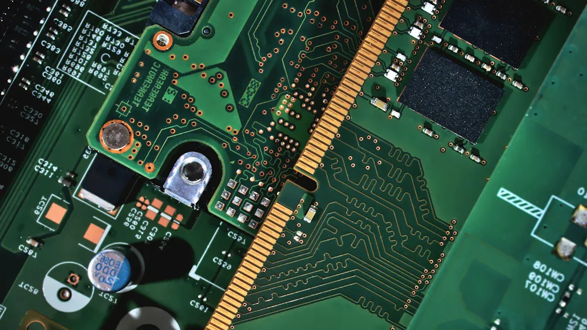
Professional pcb design services deliver complete technical packages to transform electrical schematics into physical circuit boards. Choosing expert pcb design services ensures smooth hardware fabrication and avoids expensive factory mistakes. You receive complete production files that detail all design parameters and manufacturing parameters. Engineering services facilitate quick project transfers by providing unified documentation sets and detailed layout designs.
Fabrication and Drill Data Package
Your fabrication package provides every physical detail that board fabricators need for production. You receive Gerber RS274X or ODB++ files that contain layer specifications for copper traces, solder masks, and silkscreen layers.
| Aspect | Gerber (Traditional) | IPC-2581 (Streamlined) |
|---|---|---|
| File Structure | Requires 20-30 separate files for layers, drills, and assembly data | Single XML-based file containing all design data (copper layers, drill, netlist, BOM, assembly) |
| Embedded Intelligence | 2D images with no design intent or material specs | Rich metadata: stack-up details, impedance requirements (e.g., 100Ω differential pairs), dielectric constants (e.g., FR-4 with Dk 4.2) |
| Error Prevention | High risk of mismatched or missing files causing delays/defects | Consolidated data with validation checks minimizes miscommunication and missing information |
| Collaboration | One-way data transfer | Bidirectional communication enabling manufacturer feedback (e.g., flagging unmanufacturable trace widths below 0.15mm) before production |
Exporting ODB++ files puts all CAD data, process parameters, and manufacturing workflow details into a single ZIP file. Modern IPC-2581 formats stream design data through one XML file that includes impedance routing requirements like 100Ω differential pairs. Signal routing paths require precise routing strategies to protect high-speed lines.
Missing drill files or ambiguous layer labeling will halt factory production instantly.
Fabrication data packages include Excellon ASCII drill files that define hole sizes, tolerances, and plating status. Proper drill files prevent drill bits from cutting into copper traces. Clear layer stackup drawings detail dielectric thicknesses and copper cladding weights. Engineers also verify finished signal traces and board outlines to protect pcb functionality. Top pcb manufacturing services rely on these precise routing clearances and files to maintain high manufacturing efficiency. Reliable pcb prototyping services help engineers test initial hardware quickly through fast prototyping turnaround.
Assembly Drawings, BOM, and CAD Source Files
Complete assembly documentation ensures correct component placement across every pcb board. Your Bill of Materials (BOM) provides essential procurement data for part sourcing.
- Reference designators like R1 or U1 mark exact part locations on the pcb stackup.
- Manufacturer part numbers specify exact components to eliminate purchasing errors.
- Component descriptions define electrical values, tolerances, and design intent.
- Package footprint types specify physical dimensions like 0402 or SSOP-8.
- Quantity fields track required component counts for overall design budgeting.
Pick-and-place files coordinate directly with assembly drawings to guide automated component placement machines. These files provide accurate placement coordinates on the pcb surface, including Mid X and Mid Y positions, board layer views, and part rotation angles. Assembly drawings provide visual layout verification for factory operators. These drawings show part placement orientation, like IC pin 1 indicators or LED polarity symbols. They also detail strict soldering rules and special adhesive needs.
Your deliverable package includes 3D STEP models along with native schematic and layout source files. Linking 3D STEP models inside the pcb design allows visual checking for mechanical enclosure fit. This integration verifies trace routing clearances and protects traces against physical interference while matching design requirements. Assembly services streamline electronic production across the overall design workflow, while turnkey services bring your ideas to market. Complete deliverable packages help KING FIELD execute smooth one-stop pcb assembly under strict ISO9001 and IATF16949 quality standards.
Strategic Advantages of KING FIELD PCB Layout Solutions
Accelerated Development and Reduced Rework
You shorten development cycles with an experienced pcb manufacturer. Early design reviews fix hidden flaws before physical pcb layout creation starts. Experienced pcb engineers catch component design flaws and signal integrity issues early. This proactive step prevents expensive revision cycles and reduces factory rework.
By consolidating all processes with one supplier, customers can experience improved communication, quicker problem-solving, and reduced overall costs.
Turnkey pcb design services streamline hardware execution by identifying routing bottlenecks immediately. Advanced software runs automated design rule checks. The team secures your overall signal integrity through precise impedance planning during wire routing. Early testing protects sensitive routing lines against electromagnetic interference. Design teams align every schematic with manufacturing requirements.
- Early flaw identification: Senior design engineers spot placement mistakes before fabrication.
- First-pass optimization: Experienced design teams eliminate bottlenecks to pass checks on your first attempt.
- Automated rule validation: PCB design software catches trace spacing errors early.
Rapid prototyping allows quick physical testing in real conditions. Fast turnaround pcb prototyping services help you validate custom pcb design choices quickly. You resolve placement issues before full factory production.
| Certification | Reliability Role |
|---|---|
| ISO 9001:2015 | Validates quality management systems for consistent manufacturing |
| IATF16949 | Guarantees quality and security for automotive electronics |
KING FIELD bridges the gap between initial pcb prototyping and volume creation. Our pcb manufacturing services follow strict quality standards, including RoHS compliance. Integrated engineering teams optimize every layout for seamless assembly. You achieve faster launches with dependable performance.
Expert pcb layout services transform your schematic ideas into physical hardware. Professional pcb design services bridge the gap between circuit theory and real pcb production. You protect your electronic design project from costly manufacturing delays through accurate drill files and Gerber data packages. Clean design documentation eliminates factory confusion and prevents production mistakes.
Partnering with an experienced team speeds up your pcb development cycle. KING FIELD combines precise pcb layout design with full turnkey production support. You receive top quality design check reviews and fast pcb prototype creation. Contact KING FIELD today to start your next pcb design and assembly project.
FAQ
What deliverables do professional pcb design services provide?
You get complete Gerber files, NC drill data, and ODB++ packages. These files detail copper traces, layer stackups, and drill holes. You also receive a full BOM to check pcb hardware design parameters before factory manufacturing starts.
Why does part placement matter during circuit board layout?
Smart component placement lowers electrical noise and keeps your pcb from getting too hot. Good placement keeps hot power parts away from cool chips. This clean setup shortens trace lines, improves signal routing paths, and keeps signal integrity safe across your pcb board.
How does pcb layout design protect signal integrity?
Good design matches target line impedance and stops noise reflections. Engineers draw short differential traces right beside reference ground planes. Controlled routing cuts down loop areas and protects important signal paths on your pcb.
Which software tools support your custom pcb layout services?
KING FIELD engineers use Altium, Cadence, and Mentor Graphics for pcb layout projects. Our design team turns your pcb schematics and traces into accurate physical board files. We offer fast prototyping turnaround times as short as 7 days for custom design samples.
Can KING FIELD assist with flexible design services on site?
Yes, we offer flexible talent dispatch services. Our engineers work right at your building during key design steps to help your team. This support speeds up routing fixes and improves your overall pcb design project.