 English
 Arabic
 Chinese (Simplified)
 Dutch
Dutch French
 German
 Italian
 Portuguese
 Russian
 Spanish

Yes, capacitors are attached to BGA devices using a careful process: solder paste printing, pick-and-place, reflow soldering, and inspection. This bga assembly method keeps power steady for high-speed electronics. Decoupling capacitors are very important. Placing them on the bottom side of the bga pcb assembly lowers inductance and boosts signal quality. You get a practical guide covering capacitor choice, assembly steps, issues like tombstoning, and reliability checks. The BGA design depends on these methods. The BGA structure needs careful assembly to keep working well.
Key Takeaways
- Put decoupling capacitors on the bottom of the PCB. This makes the current path shorter and reduces inductance. You get better signal quality.
- Pick MLCCs for high-frequency noise removal. They have low ESL and respond quickly. Tantalum capacitors store a lot of energy, but they filter poorly above a few megahertz.
- Control the reflow profile carefully. Use a peak temperature of 235–250°C for 30–60 seconds. This makes sure the solder joints are strong and the BGA is not harmed.
- Use X-ray to check hidden solder joints. It finds voids, cracks, bridging. This step makes sure of reliability.
- You can stop tombstoning by heating the board more slowly at first. Aim for 1.0–2.0°C each second and let the soak time last longer. This way, the heat spreads evenly.
BGA Decoupling Capacitors
MLCCs and Tantalum Capacitors
You have two main capacitor families for bga decoupling: multilayer ceramic capacitors (MLCCs) and tantalum capacitors. MLCCs are best for high-frequency decoupling because they have low equivalent series inductance (ESL) and fast response. Tantalum capacitors give higher capacitance values for storing bulk energy, but they cannot filter noise above a few megahertz well. For most bga pcb assembly designs, you will pick MLCCs for local decoupling and use tantalum parts for voltage regulation help.
Package size directly affects performance. The table below shows typical ESL values for common MLCC packages:
| Package Size | Typical ESL (nH) | Typical Value Range | Best Application |
|---|---|---|---|
| 0805 | 0.5–1.0 | 1 µF to 10 µF | Bulk decoupling |
| 0402 | 0.3–0.5 | 10 nF to 100 nF | Local IC decoupling |
| 0201 | ~0.3 | 100 pF to 10 nF | High-speed, >100 MHz decoupling |
The 0402 package is a good choice for bga designs. Its lower ESL raises the self-resonant frequency, so it can filter into the gigahertz range. You also need to think about derating. DC bias lowers effective capacitance, especially in small packages like 0402. Temperature also matters. X5R capacitors lose stability above 85°C, while X7R parts work up to 125°C with better consistency. For bga components near hot spots, pick X7R or X6 dielectrics and check capacitance under real bias conditions.
Understanding Decoupling Capacitor Placement
Placement decides how well your decoupling network works. You should mount high-frequency MLCCs on the bottom side of the PCB, right under the IC power-pin area. This bga assembly method shortens the high-frequency current path. Short connections and low-inductance vias lower mounting inductance compared to topside placement, where longer vias add more parasitic inductance in the current loop.
Via placement also matters. Put vias on the sides of capacitor pads rather than on the ends. Side placement lowers ESL by about 200 pH for a two-via setup. Adding parallel vias reduces inductance further. For a 1206 footprint, four vias between pads cut ESL by 53% compared to two vias. For 0603 and smaller packages, you lack space between pads, so put vias next to pad edges. A four-via design gives about half the ESL of a two-via design. Tightly pair power and ground vias to reduce loop inductance. For bga design, focus on via-in-pad structures to shorten the distance between power pins and capacitors. These processes directly improve signal integrity in high-speed electronics. Every assembly decision you make affects the final performance of your bga pcb assembly.
The BGA Assembly Process
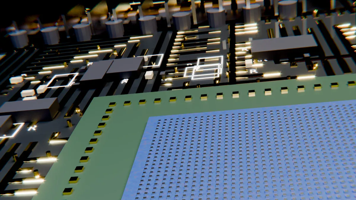
The bga assembly process follows a careful order. Each step depends on the one before it. You must control every stage well to get strong solder joint formation.
Solder Paste and Placement
Solder paste printing begins the process. You put solder paste through a stencil onto the PCB pads. The size of the stencil openings matters. For fine-pitch BGAs with 0.5 mm pitch or less, use a 1:1 opening-to-pad size. For wider 0.8 mm pitch, make the opening 0.95 times the pad width. Standard BGAs with pitch above 1.0 mm need a round opening that is 0.05 mm smaller than the pad. Ceramic BGAs need a larger opening, increased by 0.05–0.08 mm, to handle heat expansion differences.
The solder mask thickness also changes how paste is placed. Uneven mask thickness over 1.5 mils (38 µm) causes uneven paste and gaps. You want a smooth mask between 0.8 and 1.2 mils (20–30 µm) for best bga pcb assembly results.
You must control the room during solder paste printing. Keep temperature at 20°C–25°C and humidity at 40%–60%. These settings stop the paste from changing thickness, which can cause printing problems. Clean the stencil every 5 to 10 prints to stop paste from piling up in openings. Buildup leads to too little solder and bridges in solder balls.
After printing, the pick-and-place machine puts each capacitor and the BGA device in place. New machines place parts with 15 µm accuracy. This precision keeps defect rates below 0.01% in normal conditions. Feedback systems check the actual position against the design data in less than 2 ms. These systems adjust the nozzle rotation and force, stopping skew errors.
Reflow Soldering for BGA
Reflow soldering melts the solder paste and solder balls to make strong connections. The BGA package has short leads, which lowers inductance and boosts high-frequency work. This design benefit only works if the reflow process makes good joints.
You need a careful temperature plan with four zones. The preheating zone slowly raises heat to 100–150°C over 60–90 seconds. This stops thermal shock. Keep the heating rate at 1–3°C per second during preheating. The soaking zone holds temperature at 150–180°C for 60–120 seconds. This turns on the flux and removes oxidation.
The reflow zone reaches a top temperature of 235–250°C for 30–60 seconds. For lead-free Sn-Cu solder, the peak must be 18–33°C above the 217°C melting point. Keep the peak below 250°C to avoid BGA damage. The time above melting should be 30–60 seconds. Too short gives cold joints; too long gives solder balls or pad lift.
The cooling zone lowers temperature from 250°C to 100°C over 60–90 seconds. Fast cooling stops too much intermetallic compound from forming. Keep the IMC layer at 5 µm or less for strong joints.
Different reflow profiles work for different needs. The Ramp-Soak-Spike (RSS) profile uses a 2–4°C/s rate and cuts down voids in BGA joints. The Ramp-to-Spike (RTS) profile uses a 1–3°C/s rate and reduces head-on-pillow defects. Pick based on your paste chemistry and part needs.
Controlling moisture in PCBs before assembly is very important. Baking removes water that the board has soaked up. This water can cause solder defects like popcorning, especially in BGAs.
These processes work for standard boards and advanced 3d stacked bga assembly setups. Each assembly step needs careful work. The bga pcb assembly flow links capacitor placement with solder balls using careful heat control. Your electronics rely on this careful balance. Every bga assembly choice affects the final reliability of your product.
BGA Assembly Inspection and Testing
X-Ray Inspection for Solder Joints
X-ray inspection shows what your eyes cannot see under the bga package. Visual checks and automated optical inspection only look at surface features. The solder balls stay hidden under the device, so you need penetrating imaging to check solder joint quality. X-ray systems find voids, cracks, bridging, and misalignment that would otherwise go unnoticed until field failure.
For fine-pitch bga assemblies, you need sub-micron resolution. Standard microfocus tubes offer focal spot sizes of 5 µm or less. High-end nanofocus systems achieve under 1 µm. This resolution determines the smallest void you can detect within each ball. Without it, small defects pass through inspection unnoticed.
Common defects you will encounter include:
- Voids: Air pockets trapped inside solder balls, often from flux outgassing. Voids larger than 25% of ball volume weaken the joint considerably.
- Cracks: Fractures from thermal stress or mechanical shock, causing intermittent connections.
- Bridging: Excess solder creating unintended connections between adjacent balls, leading to shorts.
- Misalignment: Balls not centered on PCB pads, reducing contact area and risking open circuits.
- Head-in-pillow defects: Solder ball and paste fail to coalesce, creating a weak bond.
X-ray also reveals solder mask defects and alignment problems invisible to surface inspection. Damaged masks cause improper solder flow, showing as excessive solder between balls. Misplaced components produce uneven or stretched ball shapes. These issues occur beneath the package, so X-ray remains the only reliable detection method.
Popcorning presents another challenge. Moisture trapped in the polymer molding converts to steam during reflow, expanding the package like popcorn. This expansion can press on liquid solder, causing bridging between adjacent balls. Lead-free solders increase this risk due to higher reflow temperatures, raising moisture sensitivity levels by one to three levels.
Electrical Testing and Validation
X-ray confirms physical integrity, but electrical testing proves functionality. You need both for complete bga pcb assembly validation. In-circuit testing checks each connection for opens and shorts. Boundary scan testing verifies digital signal paths through the bga device itself.
Functional testing exercises the complete electronics under real operating conditions. You apply power, send test signals, and measure responses. This step catches issues that structural inspection misses, such as marginal connections that pass X-ray but fail under load.
The assembly process does not end at the reflow oven. Your inspection and testing processes determine whether the bga assembly meets reliability standards. Each test adds confidence that your solder paste printing and reflow parameters produced sound joints. For mission-critical applications like aerospace or medical devices, void limits tighten from 30% down to 10%. You must adjust your acceptance criteria based on your industry requirements.
BGA Assembly Challenges and Solutions
Tombstoning and Misalignment
Tombstoning is one of the most annoying problems in bga pcb assembly. A small capacitor stands up on one end during reflow, and the connection breaks completely. This happens because solder paste on one pad melts just before the other pad. The uneven wetting force then pulls the part upright.
Several things cause this issue. Uneven solder paste application puts more paste on one pad. Uneven heating happens when a PCB has unbalanced copper distribution. Mismatched pad sizes create unequal thermal mass. The table below lists the main causes:
| Cause | Description | Impact |
|---|---|---|
| Uneven heating | One pad melts earlier | Creates imbalance in solder wetting |
| Asymmetric pad design | Unequal pad size or shape | Uneven thermal mass |
| Solder paste issues | Wrong volume or uneven printing | Poor wetting force balance |
| PCB thermal imbalance | Unequal copper distribution or routing | One pad heats slower |
| Component size | Small MLCC/resistors | Higher sensitivity to surface tension |
| Reflow profile issues | Fast ramp or poor soak control | Uneven solder melting |
| Contamination | Oxidation or moisture in paste/pads | Weak solder bonding |
If multiple 0402 parts across different board areas tombstone, you likely have a profile issue, not a paste issue. Your ramp rate hits the board too fast. Lower your preheat ramp rate to 1.0–2.0°C/sec and extend the soak time so the temperature becomes perfectly uniform.
Misalignment is another related challenge. You can prevent many placement errors with smart pad design. Put decoupling capacitors on the bottom side directly under the bga package. This shortens the power-loop path and lowers inductance. Use short via pairs and multiple ground vias to connect each capacitor to the bga power and ground balls. Avoid long dog-bone power pin fanouts because they add loop inductance. Design your fanout and decoupling placement together, not one after the other, so the bottom layer has enough room.
Thermal Stress and Reliability
Thermal stress threatens long-term reliability in every bga assembly. The bga package, PCB, and nearby capacitors all expand at different rates when heated. This mismatch creates mechanical strain on solder balls during each power cycle. Over time, this strain causes fatigue cracks that hurt solder joint quality.
Underfill material offers a strong solution. This epoxy flows under the bga package after reflow and hardens. It reduces solder joint fatigue from thermal expansion mismatch between the component and PCB. Underfill also spreads mechanical stress more evenly from the solder balls across the whole package-board system. This greatly improves thermal cycling performance.
Your reflow profile directly affects thermal stress resistance. A controlled cooling zone prevents too much intermetallic compound from forming. Keep the IMC layer thin for stronger joints. These processes apply equally to standard boards and advanced 3d stacked bga assembly setups.
Every assembly decision you make affects final reliability. Solder paste printing quality, placement accuracy, and thermal control all matter. Your electronics depend on this careful balance. The bga design rewards precision at every step. Proper bga pcb assembly techniques help your product survive years of thermal cycling without failure.
Your bga assembly work moves through four stages: capacitor selection, bottom-side placement, reflow soldering, and inspection. The short leads of a bga device reduce inductance naturally. This design benefit makes proper decoupling capacitor placement even more critical. Your bga pcb assembly process balances material science with precision engineering. Each stage builds on the one before it. Poor capacitor selection leads to power noise. Bad placement adds inductance. Wrong reflow settings create weak joints. Every bga depends on this careful sequence. The electronics you build rely on it. Could a single misaligned capacitor ruin the performance of your high-speed bga design? A part that shifts by just 0.1 mm changes the current path. The answer shows why every detail matters in assembly.
FAQ
Why do you place decoupling capacitors on the bottom side of the board?
You put them right under the BGA power pins. This makes the current path shorter between the capacitor and the IC. Shorter paths mean lower inductance. Lower inductance makes signal quality better in your high-speed electronics. The bottom-side spot works best for this job.
What causes tombstoning during bga assembly?
Tombstoning occurs when solder paste on one pad melts before the other pad. Uneven heating, mismatched pad sizes, or bad paste printing cause this issue. You can fix it by slowing your preheat ramp rate to 1.0–2.0°C per second and making the soak time longer.
How does X-ray inspection help with bga components?
X-ray lets you see solder joints hidden under the package. You can find voids, cracks, bridging, and misalignment that visual checks miss. For fine-pitch ball grid array devices, you need sub-micron resolution to spot small defects. This inspection step keeps your final product quality safe.
Can you use the same reflow profile for every assembly?
No. Different boards and components need different thermal profiles. The Ramp-Soak-Spike profile cuts down voids in solder joints. The Ramp-to-Spike profile stops head-on-pillow defects. You must match your profile to your paste chemistry and component needs. Your bga pcb assembly quality depends on this choice.
What role does underfill play in 3d stacked bga assembly?
Underfill epoxy flows under the package after reflow and hardens. It lowers solder joint fatigue from thermal expansion mismatch. The material spreads mechanical stress evenly across the package-board system. This process boosts thermal cycling performance a lot. Your assembly processes gain from this extra protection.