 English
 Arabic
 Chinese (Simplified)
 Dutch
Dutch French
 German
 Italian
 Portuguese
 Russian
 Spanish

A heavy copper PCB uses thick metal foil over 3 oz/ft², with 2 oz/ft² or more as the basic starting point, to reduce heat loss when sending strong electric currents. On the other hand, High-Density Interconnect technology uses thin copper foils under 1 oz or 35 µm with microvias to fit signal paths into tiny spaces. Car engineers pick circuit designs based on exact electrical needs. Designing a great automotive PCB for EV applications means looking at current capacity, heat control, saved space, building difficulty, and total cost balances. These careful tests guarantee great power delivery and dependable performance in important vehicle electronic systems.
Key Takeaways
- Heavy copper PCBs use thick metal lines to carry strong electric currents safely.
- Thick copper PCB lines lower electricity resistance and quickly cool down power parts.
- HDI technology uses tiny drilled holes and thin wires to fit control circuits into small spaces.
- Engineers combine thick copper and HDI layers on single boards for small hybrid designs.
Heavy Copper Automotive PCB for EV Applications
Ampacity and Thermal Dissipation
Engineers choose heavy copper foil weights from 2 to 20 oz/ft² for heavy copper pcb traces. These thick metal paths lower electrical resistance across internal traces on an automotive pcb for ev applications. Less resistance lowers heat buildup and stops sudden voltage drops during high current loads. Electrodeposited copper offers a high thermal conductivity of 401 W/(m-K). This natural property helps thick copper planes move heat away from active power parts fast. Heavy copper pcb manufacturing turns internal copper layers into efficient flat heat sinks.
Standard circuit boards rely on thin copper foils below 2 oz/ft². A direct comparison of heavy copper vs standard pcb designs shows clear benefits for heat management. Heavy copper pcb manufacturing boosts the max current carrying capacity without making surface traces wider. Specialized heavy copper pcb manufacturing also builds board strength against physical stress and severe thermal expansion. IPC-6012DS and IPC-6012FA standards guarantee board toughness during harsh vibration and thermal cycling. Thermal management stays simple because heavy copper pcb manufacturing removes heavy external wire buses.
Subsystems in High Power EVs
Electric vehicle systems use heavy copper pcb designs to send large currents safely through the vehicle. Key subsystems like power inverters and motor controllers send power directly to drive motors. On-board chargers handling 11 kW power levels use these sturdy boards to keep steady thermal performance. Heavy copper pcb manufacturing allows smooth power flow inside compact dc-dc converters. Power distribution systems also use thick copper structures instead of heavy wiring harnesses. These assemblies easily handle high power applications throughout the drive chassis.
High power applications demand great board reliability under harsh driving conditions. Heavy copper pcb manufacturing improves the battery management system power rails. Specialized heavy copper pcb manufacturing powers extra energy units and high-voltage charging systems. These electric drive subsystems create strong high power requirements. Heavy copper pcb manufacturing delivers great thermal performance and reliable electrical execution across all car systems.
HDI Technology for EV Signal Density
Microvias and Fine Trace Routing
High-Density Interconnect designs use thin copper foils measuring 35 µm or less to craft intricate circuit boards. Engineers place laser-drilled microvias smaller than 0.15 mm wide to join nearby board layers. Circuit builders use IPC-2226 for layout rules and IPC/JPCA-2315 for microvia design, while choosing parts with IPC/JPCA-4104 rules. Modern HDI factory methods make fine line widths and spaces under 50 µm to route tight trace grids.
| Via type | Definition or aspect ratio |
|---|---|
| Microvia | Laser-drilled interconnect with aspect ratio 1:1 or less |
| Blind via | Connects outer layer to inner layer without passing through board |
| Buried via | Connects internal layers only with aspect ratio below 8:1 |
Makers limit stacked microvias to two levels because heat growth causes physical stress. Designers choose staggered microvias over three or more layers to boost long-term hardware strength. Build rules match IPC-6012 for stiff boards and IPC-6013 for flexible circuits, while high-frequency units use IPC-6018 rules. Tiny target pads and capture pads save valuable board space and speed signal flow past large BGA packages.
Control Units and BMS Logic
Modern self-driving car electronics need quick signal processing alongside strict noise protection. ADAS control units must protect high-frequency signal health while keeping power loss under 0.5 dB/cm at 2 GHz. Microvia routing shortens total trace lengths while cutting trace crosstalk down to -60 dB or less. Main computer chips use these tight routing rules to squeeze control circuits into small modules.
All battery management system setups need exact tracking for cell voltages and pack temperatures. The battery management system uses dense HDI logic layers to run chips right next to loud electrical parts in power systems. Shielding layers supply 80 to 100 dB EMI noise protection to block high-frequency signal disruption. This strong noise blocking works from 100 MHz to 10 GHz to protect EV safety systems and maintain steady low power signals.
Heavy Copper vs HDI for High Power EVs
Thermal and Electrical Performance
Engineers compare heat control and current capacity when picking circuit layouts for modern electric vehicles. Heavy copper pcb manufacturing uses thick metal layers to safely carry higher electrical current across power circuits. These thick conductors send energy efficiently while keeping nearby components cool during operation. Thick copper layers lower the electrical resistance across internal traces. Low trace resistance stops heat from building up during continuous power delivery. The tough design cuts energy loss in an automotive pcb for ev applications without needing bulky heatsinks or extra cooling parts. A direct test of heavy copper vs standard pcb designs shows better heat control in thick trace layouts. Heavy copper pcb manufacturing builds flat thermal channels that quickly move heat away from high-power parts.
High-Density Interconnect designs focus on squeezing tight signal paths into small spaces rather than carrying massive electrical current. Narrow line widths and small laser microvias shrink control circuits into tiny physical board areas. However, thin HDI foil carries far less power than thick copper lines. High power currents cause extra heat on thin HDI layers, while heavy copper pcb manufacturing offers stable thermal performance during heavy current output. Designers balance tight space limits against total power needs in modern car systems. Heavy copper pcb manufacturing guarantees steady power flow across heavy load circuits without heat failure during peak usage. High current traces need thick metal parts to keep resistance low and protect car safety in all driving conditions. Engineers select HDI boards for logic control units that need high pin counts and small circuit footprints.
Cost and Manufacturing Yield
Building these circuit boards creates different factory challenges for each technology. Heavy copper pcb manufacturing needs longer chemical etching times to strip thick metal from between circuit lines. Etching thick copper forces factory machines to run much slower inside chemical bath tanks. Filling gaps between deep trace channels needs special lamination steps to stop air bubbles inside inner layers. Inspectors check trace edges under microscopes to make sure side walls remain smooth and clean. On the other hand, HDI manufacturing uses precise laser microvia drilling tools and complex repeated lamination steps.
| Evaluation Metric | Heavy Copper PCB | HDI PCB |
|---|---|---|
| Layer count range | 2 to 8 layers | 4 to 18+ layers |
| Mechanical durability | High structural rigidity | Flexible thin stackup |
| Relative unit cost | Moderate production cost | Higher tooling and processing cost |
| Thermal cycling yield | Lower stress thermal performance | Higher microvia thermal stress risks |
Heavy copper pcb manufacturing strengthens board durability against hard bumps, rough road vibration, and car body motion. Heavy copper pcb boards easily pass tough car vibration tests under AEC-Q200 standards. Small microvias inside HDI boards suffer heat stress during extreme hot and cold weather cycles. This stress can increase system failure rates over long driving lifespans. Heavy copper pcb manufacturing provides higher factory output for high-current electric power distribution units. Automotive test engineers check board toughness under strict hot and cold temperature tests. Heavy copper builds resist heat wear while protecting internal wire paths from physical cracking. Modern hybrid designs mix both methods when systems need dense signal paths right next to raw power lines. Heavy copper pcb manufacturing improves power flow, while HDI layers handle fast control logic commands inside tiny spaces.
Hybrid Heavy Copper and HDI Solutions
Combined Stackup Architectures
Modern electric vehicles need advanced circuit board layers. Engineers mix heavy copper layers with thin interconnect layers inside one board. Thick inner layers send huge currents through high power systems. Meanwhile, thin outer layers move quick signals from small computer chips. Heavy copper pcb manufacturing joins these different copper sizes during careful building steps. Factory teams fill big spaces around thick copper lines using fluid resin glue. This glue stops clear air bubbles inside the pressed center.
Hybrid layers save precious circuit space inside tiny car compartments. Heavy copper pcb manufacturing fits power lines directly inside internal board sections. External microvias join tight control chips straight to internal power layers. This design removes extra wiring bundles inside motor drive units. Heavy copper pcb manufacturing cuts total build weight across high-voltage drive units. Car factories make these mixed boards using normal material like high-Tg FR-4. The finished layers offer great electrical division between power lines and fragile signal paths.
Rigid-Flex Design Integration
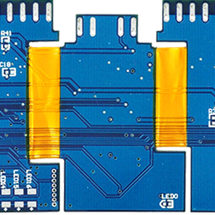
Rigid-flex circuit setups give great layout options for vehicle hardware teams. Designers mix tough heavy copper pcb parts with bending plastic circuit strips. Heavy copper pcb manufacturing glues thick copper parts onto thin flexible base sheets. The stiff parts hold heavy power parts inside the battery management system. The flex parts turn around tight spots inside vehicle frames. This smart bending cuts building mistakes during car assembly.
Heavy copper pcb manufacturing must follow IPC-6013 Class 3 standards to ensure long-term reliability in dynamic automotive environments.
Subsystem Zone,Copper Foil Thickness,Primary Functional Role
Power Section,3 to 10 oz/ft²,High Current Transmission
Control Section,0.5 to 1 oz/ft²,Dense Microvia Logic Routing
Flex Interface,1 oz/ft² Polyimide,Dynamic Chassis Bending
Heavy copper pcb manufacturing adds physical strength to strong wire connection spots. Moving flex cables replace standard plug parts between inside electronic boxes. Designers get physical freedom while saving valuable setup space inside tiny motor covers. Heavy copper pcb manufacturing shields weak inner circuits against sudden temperature changes. Electric car makers use these joined designs to get ideal heat control and top space savings.
Choosing the right design requires clear evaluation of electrical current limits, thermal management, power density, and space boundaries. Automotive hardware engineers follow a clear decision process:
- Determine total power needs for the electric car subsystem.
- Choose heavy copper pcb manufacturing to handle heat performance.
- Select HDI technology for tight signal trace routing.
- Combine both using hybrid heavy copper pcb manufacturing for one vehicle board.
Early vendor collaboration optimizes heavy copper pcb manufacturing workflows. Heavy copper pcb manufacturing reviews reduce overall production costs. Smart heavy copper pcb manufacturing adjustments improve factory yield. Proven heavy copper pcb manufacturing testing protects durability across the automotive industry. Reliable heavy copper pcb manufacturing safeguards your automotive pcb for ev applications. Heavy copper pcb manufacturing improves total system reliability.
FAQ
What defines a heavy copper pcb in electric vehicles?
A heavy copper pcb uses thick foil weighing over 3 oz/ft². Special heavy copper pcb manufacturing creates wide pathways to move extreme heat across an automotive pcb for ev applications. Wise heavy copper pcb manufacturing also cuts trace resistance. Proven heavy copper pcb manufacturing ensures steady power delivery inside the car.
How does heavy copper vs standard pcb performance differ in high power applications?
Checking heavy copper vs standard pcb designs shows better heat control in thick metal choices. Standard boards use thin foils under 2 oz/ft². Custom heavy copper pcb manufacturing allows steady work in high power applications. Precise heavy copper pcb manufacturing prevents dangerous heat damage near active drive circuits.
Why do battery management system designs use hybrid boards?
A modern battery management system needs tight logic routing right next to heavy power rails. Dedicated heavy copper pcb manufacturing creates thick power paths for high-voltage charging systems. At the same time, heavy copper pcb manufacturing includes tiny HDI microvias. This smart mix protects low-power signals across the battery management system.
How does board architecture impact field failure rates in EVs?
Heat stress during hot cycles increases field failure risks inside tiny microvia designs. Heavy copper pcb manufacturing offers strong board strength against rough car vibration. Custom heavy copper pcb manufacturing meets AEC-Q200 standards with ease. Advanced heavy copper pcb manufacturing protects internal trace integrity across harsh driving environments.