What Makes Multilayer PCBs Unique and Efficient
Multilayer PCBs revolutionize modern electronics with their compact design and exceptional efficiency. Their structure, composed of multiple conductive and insulating layers, allows you to achieve higher circuit density and better signal integrity. These features make them indispensable for creating smaller, more advanced products like smartphones and micro projectors.
The advantage of the multilayer PCB circuit board is that the lines can be distributed in multiple layers to be designed more precisely. This allows for smaller products to be realized, such as mobile phone circuit boards and micro projectors, while also increasing design flexibility and better control over signal integrity.
Key benefits include reduced board size, improved electromagnetic interference (EMI) shielding, and enhanced reliability. Multilayer PCBs accommodate complex circuits, supporting the trend toward miniaturization and high-speed applications. Their ability to handle intricate designs makes them a cornerstone of technological innovation.
Key Takeaways
- Multilayer PCBs help create smaller designs, making them key for modern gadgets like phones and medical tools.
- These PCBs improve signal quality and cut down on interference, ensuring they work well in fast systems.
- Their layered design handles tricky circuits, helping make tiny devices without losing features.
- Though they have many benefits, multilayer PCBs cost more and take longer to make, which designers should think about.
- Good design and picking the right materials are important to make multilayer PCBs last and work well in tough conditions.
What Is a Multilayer PCB?
Definition and Features
A multilayer PCB is a type of printed circuit board that consists of three or more conductive layers stacked together. These layers are separated by insulating materials and bonded into a single, compact structure. This unique design allows you to create intricate circuit layouts in a smaller space, making it ideal for modern electronic devices.
Key features of multilayer PCBs include:
- High Component Density: By utilizing inner layers for circuit traces, these PCBs support more components in less space.
- Improved Signal Integrity: The layered structure ensures signals maintain their strength and quality.
- Electromagnetic Shielding: Proper placement of power and ground layers enhances shielding against electromagnetic interference (EMI).
- Controlled Impedance: This feature ensures consistent electrical performance, reducing signal loss.
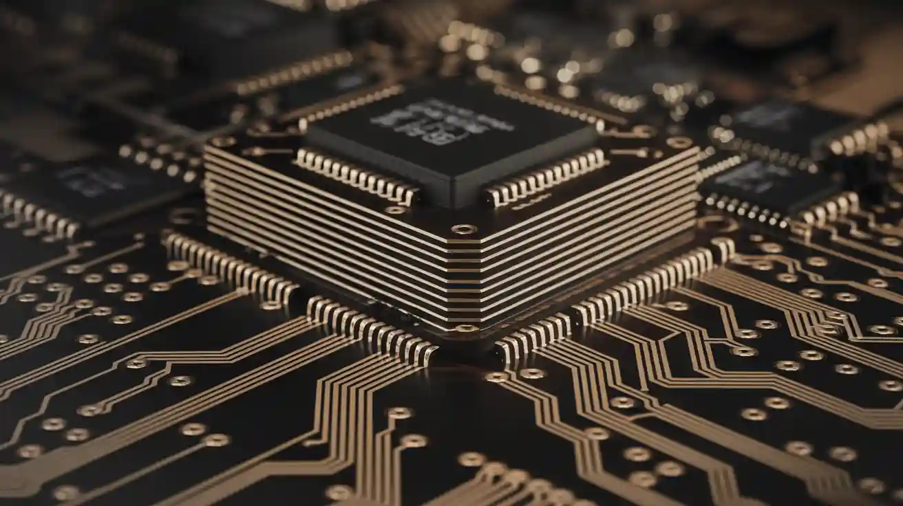
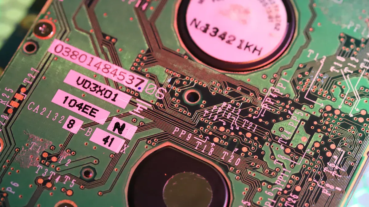
The structure of a multilayer circuit board includes an inner core surrounded by alternating layers of conductive copper and insulating material. Copper-plated holes, known as vias, connect the layers electrically, enabling seamless communication between components.
Comparison with Single- and Double-Layer PCBs
When comparing multilayer PCBs to single- and double-layer PCBs, the differences become clear. Single-layer PCBs have only one conductive layer, while double-layer PCBs feature two. Multilayer PCBs, on the other hand, consist of three or more layers, offering significantly higher functionality.
| Feature/Type | Single-Layer PCB | Double-Layer PCB | Multilayer PCB |
|---|---|---|---|
| Number of Layers | One conductive layer | Two conductive layers | Three or more conductive layers |
| Component Density | Low | Moderate | High |
| Signal Integrity | Basic | Improved | Superior |
| Size | Larger | Smaller | Compact |
| Applications | Simple devices like calculators | Consumer electronics like radios | Advanced gadgets like smartphones |
Multilayer PCBs excel in applications requiring high-speed, high-density circuits. Their compact design and advanced features make them indispensable in industries like telecommunications, medical devices, and aerospace systems.
Tip: If you’re designing a product that demands high performance and minimal size, a multilayer PCB is your best choice.
Structure of a Multilayer PCB
Core and Prepreg Layers
The core and prepreg layers form the backbone of a multilayer circuit board. The core is a rigid, pre-laminated sheet of fiberglass reinforced with epoxy resin and copper foil. It provides structural stability and serves as the foundation for the conductive layers. Prepreg, on the other hand, is a semi-cured fiberglass material impregnated with resin. It acts as both an insulating layer and a bonding agent between the core and other layers.
Key properties of these materials include:
- Resin Content: Determines the thickness and dielectric properties of the laminate.
- Mechanical Strength: Ensures rigidity and resistance to flexing stresses.
- Dimensional Stability: Minimizes expansion during manufacturing, ensuring precise alignment of layers.
Prepreg’s malleability before lamination allows for flexibility during assembly, while its cured state provides strong insulation and bonding. Together, the core and prepreg layers ensure the structure and composition of the PCB remain robust and reliable.
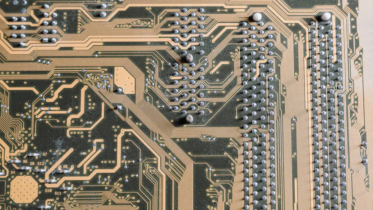
Conductive and Insulating Materials
Multilayer PCBs rely on a combination of conductive and insulating materials to achieve high performance. Conductive layers, typically made of copper, form the circuit traces that carry electrical signals. These layers are separated by insulating materials, such as fiberglass-reinforced epoxy or polyimide, which prevent electrical interference and maintain signal integrity.
Modern manufacturing techniques enhance the efficiency of these materials:
- Sequential Lamination: Builds the PCB layer by layer, enabling complex designs.
- Photoimageable Dielectrics: Allow for finer line resolution and smaller vias, critical for high-density circuits.
- Advanced Plating Techniques: Ensure reliable connections in high-aspect-ratio vias.
This combination of materials and techniques ensures that the PCB can handle high-speed signals while maintaining power integrity.
Role of Vias in Connectivity
Vias are essential for connecting the conductive layers in a multilayer PCB. These small, copper-plated holes allow electrical signals to travel between layers, enabling seamless communication between components. There are three main types of vias:
- Through-Hole Vias: Extend through all layers of the PCB.
- Blind Vias: Connect outer layers to one or more inner layers.
- Buried Vias: Connect only inner layers, remaining invisible from the surface.
Studies highlight the importance of vias in maintaining signal and power integrity. For example, research shows that ground vias near signal vias reduce signal distortion by providing consistent return paths. Advanced techniques, such as optical alignment systems, ensure precise via placement, further enhancing connectivity and performance.
Tip: Proper via design is crucial for minimizing signal loss and ensuring reliable operation in high-speed circuits.
Advantages of Multilayer PCBs
Space Efficiency and Compact Design
Multilayer PCBs excel in space efficiency, making them ideal for modern electronics. By stacking multiple layers of conductive and insulating materials, these PCBs allow you to fit more circuit traces into a smaller area. This compact design supports the growing demand for miniaturized devices like smartphones, wearables, and IoT-enabled products.
The increasing popularity of portable gadgets and medical devices highlights the importance of compact PCBs. For instance, multilayer PCBs integrate various components into a single structure, reducing the overall size of devices without compromising functionality. This efficiency is crucial for industries like healthcare, where space-saving designs enable advanced wearable medical instruments.
| Metric | Value |
|---|---|
| Expected Market Size by 2031 | $99.11 billion |
| CAGR during forecast period | 5.2% |
| Revenue share in consumer electronics | 27% |
The rollout of 5G technology further amplifies the need for compact, high-performance PCBs. Enhanced manufacturing processes now make it possible to achieve higher circuit densities while maintaining cost-efficiency.
High Functionality and Performance
Multilayer PCBs deliver exceptional functionality and performance, making them indispensable in high-speed and high-density applications. Their layered structure minimizes electromagnetic interference (EMI) and ensures superior signal integrity. This is particularly important for devices requiring reliable and consistent electrical performance.
Rigorous testing procedures validate the high functionality of these PCBs. Signal integrity analysis, impedance measurements, and EMI testing ensure optimal performance. Specialized design software and high-quality materials further enhance their capabilities. For example, careful layer stackup planning reduces signal loss and improves electrical performance.
The ability to handle complex circuits makes multilayer PCBs a cornerstone of modern technology. Whether you’re designing telecommunications equipment or advanced gaming devices, these PCBs provide the reliability and efficiency you need.
Durability and Reliability
Durability is a key advantage of multilayer PCBs. These boards undergo extensive testing to ensure they can withstand harsh conditions. Environmental testing evaluates their resistance to extreme temperatures, humidity, and chemical exposure. High Accelerated Temperature and Humidity Stress Testing (HAST) reveals weaknesses like delamination and corrosion, ensuring long-term reliability.
Temperature cycling tests assess the PCB’s ability to endure repeated temperature variations, identifying potential failures in solder joints and interconnections. Salt spray testing measures resistance to corrosive environments, which is critical for marine and industrial applications.
These rigorous evaluations confirm that multilayer PCBs maintain their integrity under critical conditions. Their robust structure and composition make them a reliable choice for industries like aerospace and automotive, where durability is non-negotiable.
Tip: When designing for demanding environments, prioritize multilayer PCBs to ensure long-lasting performance.
Support for Complex and High-Speed Circuits
Multilayer PCBs are essential for handling complex and high-speed circuits. Their unique structure, which includes multiple conductive and insulating layers, allows you to design intricate circuits while maintaining signal integrity. These PCBs excel in applications where high-frequency signals and dense component layouts are critical.
High-speed circuits demand precise control over electrical performance. Multilayer PCBs achieve this by minimizing signal loss and electromagnetic interference (EMI). The layered design ensures that power and ground planes provide effective shielding, while controlled impedance reduces signal distortion. This makes them ideal for advanced technologies like 5G communication systems, high-performance computing, and automotive radar systems.
To understand the technical capabilities of multilayer PCBs, consider the following metrics:
| Metric | Description |
|---|---|
| S-parameters | Measure transmission line performance across frequencies, crucial for signal integrity. |
| Surface Roughness | Impacts signal losses; understanding its metrics is essential for high-speed performance. |
| Skin Effect | Describes current flow near conductors’ surfaces at high frequencies, affecting signal quality. |
| Differential Insertion Loss | Requires meticulous measurement techniques like S21 and SDD21 for accurate assessment. |
These metrics highlight the importance of precise material selection and advanced manufacturing techniques. For example, copper roughness plays a significant role in bonding laminates and affects high-speed performance. Collaborating with PCB fabricators ensures accurate measurement techniques and optimal design outcomes.
Multilayer PCBs also support complex circuits by enabling dense routing of traces. The additional layers provide more space for signal paths, reducing the need for long, convoluted routes. This improves signal quality and reduces latency, which is critical for applications like data centers and medical imaging devices.
Tip: When designing high-speed circuits, prioritize materials with low dielectric loss and ensure proper via placement to maintain signal integrity.
The advantages of multilayer PCBs in supporting complex and high-speed circuits make them indispensable in modern technology. Their ability to handle intricate designs and maintain performance under demanding conditions ensures they remain a cornerstone of innovation.
Disadvantages of Multilayer PCBs
Higher Costs and Complexity
Multilayer PCBs come with significantly higher costs compared to simpler alternatives. The need for sophisticated materials, such as high-quality copper and advanced insulating layers, drives up production expenses. Additionally, the intricate design requirements demand skilled engineers and specialized software, further increasing costs. Manufacturing processes like sequential lamination and advanced plating techniques also add to the complexity.
For instance, the cost analysis below highlights the expense differences between various PCB types:
| PCB Type | Design Cost per Square Inch | Manufacturing Cost per Square Inch | Design Time |
|---|---|---|---|
| Simple 2-Layer | $0.50 – $2.00 | $0.10 – $0.50 | Low |
| 4-Layer | $1.00 – $3.50 | $0.20 – $0.75 | Medium |
| 6-Layer | $2.00 – $5.00 | $0.40 – $1.00 | Medium to High |
| 8+ Layer | $3.50 – $10.00+ | $0.80 – $2.00+ | High |
The increased number of layers and the need for rigorous testing and quality control make multilayer PCBs a more resource-intensive choice. While these costs are justified for high-performance applications, they may not be suitable for budget-sensitive projects.
Challenges in Repair and Maintenance
Repairing and maintaining multilayer PCBs can be challenging due to their complex structure. Identifying faults in the inner layers often requires advanced diagnostic tools and expertise. Accessing these layers without damaging the surrounding traces or components is another significant hurdle.
- Difficulty pinpointing damaged layers.
- Ensuring proper isolation during repairs to prevent short circuits.
- Maintaining electrical continuity across all layers.
Simple soldering techniques may suffice for minor repairs, but complex issues often require a systematic approach and expert intervention. For example, repairing a buried via or an internal trace demands precision and advanced equipment. These challenges make multilayer PCBs less ideal for applications where frequent maintenance is expected.
Longer Manufacturing Time
The production of multilayer PCBs takes considerably longer than that of single- or double-layer boards. Each layer requires precise alignment, lamination, and drilling, which are time-consuming processes. Advanced techniques like optical alignment systems and sequential lamination further extend production timelines.
This extended manufacturing time not only delays project completion but also contributes to higher costs. Industries relying on rapid prototyping or quick turnarounds may find this a significant drawback. However, for applications requiring high performance and reliability, the longer production time is often a necessary trade-off.
Note: While multilayer PCBs offer unmatched performance, their disadvantages—higher costs, repair challenges, and longer production times—should be carefully considered during the design phase.
Applications of Multilayer PCBs
Consumer Electronics and Gadgets
Multilayer PCBs play a pivotal role in the evolution of consumer electronics. Their compact design allows you to create smaller, more portable devices without sacrificing performance. By stacking multiple layers, these PCBs optimize electrical pathways, enabling faster and more efficient gadgets. This makes them essential for products like smartphones, laptops, and gaming consoles.
- Multilayer PCBs enhance reliability by reducing wiring errors and improving connection durability.
- They support high-speed circuits, ensuring seamless performance in advanced gadgets.
- Their ability to integrate complex circuits into a small footprint drives innovation in wearable technology and IoT devices.
The growing demand for smarter, more efficient electronics highlights the importance of multilayer PCBs. Market analysis predicts the multilayer PCB industry will reach $144.7 billion by 2032, driven by sectors like consumer electronics. This underscores their critical role in shaping the future of technology.
Telecommunications Equipment
The telecommunications industry relies heavily on multilayer PCBs to meet the demands of modern communication systems. These PCBs support high-speed data transmission and ensure signal integrity, making them indispensable for advanced equipment.
Applications include:
- Wireless communication systems and mobile phone towers.
- High-speed servers, routers, and electronic data storage devices.
- Satellite systems, video conferencing technologies, and VoIP systems.
Multilayer PCBs provide the reliability and performance needed for these applications. Their layered structure minimizes electromagnetic interference, ensuring clear and uninterrupted communication. As the industry evolves with 5G and beyond, the demand for these PCBs will continue to grow.
Medical Devices and Instruments
In the healthcare sector, multilayer PCBs enable the development of advanced medical devices. Their compact design and high functionality make them ideal for applications where precision and reliability are critical.
Examples of medical devices using multilayer PCBs include:
- Wearable health monitors and diagnostic equipment.
- Imaging systems like MRI and CT scanners.
- Surgical instruments and life-support systems.
These PCBs ensure accurate signal transmission and robust performance, even in demanding environments. Their ability to integrate multiple functions into a single board reduces device size, improving portability and usability. This makes them a cornerstone of innovation in medical technology.
Note: The diverse applications of multilayer PCBs across industries highlight their versatility and importance in modern technology.
Automotive and Aerospace Systems
Multilayer PCBs play a critical role in the automotive and aerospace industries, where reliability and performance are paramount. These sectors demand circuit boards that can withstand extreme conditions, including high temperatures, vibrations, and electromagnetic interference. The unique structure of multilayer PCBs, with their stacked layers of conductive and insulating materials, makes them ideal for such high-demand environments.
In the automotive industry, these PCBs power essential systems like engine control units, advanced driver-assistance systems (ADAS), infotainment systems, and various sensors. Their compact design allows for efficient integration into modern vehicles, where space is often limited. Additionally, the ability to route complex traces across multiple layers ensures optimal performance and signal integrity, even in high-speed applications.
The aerospace sector relies on multilayer PCBs for avionics, navigation systems, and communication equipment. These applications require extremely high reliability and performance, as any failure could have catastrophic consequences. For instance, Airbus Defense and Space awarded contracts in August 2024 for multilayer PCBs used in the Eurofighter Typhoon and A400M military transport aircraft. This highlights the trust placed in these PCBs for mission-critical systems.
| Industry | Application Examples | Requirements |
|---|---|---|
| Automotive | Engine control units, ADAS, infotainment systems, sensors | High reliability, temperature demands |
| Aerospace | Avionics, navigation systems, communication equipment | Extremely high reliability and performance |
The layered design of these PCBs also enhances durability, ensuring they can endure the harsh conditions often encountered in automotive and aerospace environments. For example, the thermal stability of the materials used in multilayer PCBs prevents warping or delamination under extreme heat. This makes them a reliable choice for applications where safety and precision are non-negotiable.
Tip: When designing PCBs for automotive or aerospace systems, prioritize materials with high thermal resistance and ensure proper layer stackup to meet stringent industry standards.
The versatility and robustness of multilayer PCBs make them indispensable in these industries. Their ability to handle complex circuits, maintain signal integrity, and endure challenging conditions ensures they remain a cornerstone of innovation in automotive and aerospace technologies.
Manufacturing Process of Multilayer PCBs
Design and Layer Stacking
The design and layer stacking phase forms the foundation of the multilayer pcb manufacturing process. During this stage, you define the number of layers and their specific functions. Each layer serves a unique purpose, such as routing signals, providing power, or acting as a ground plane. For example:
| Layer Number | Layer Type | Purpose |
|---|---|---|
| 1 | Top Signal | Primary signal routing |
| 2 | Ground Plane | Provides a reference ground for signals |
| 3 | Inner Signal 1 | Additional signal routing |
| 4 | Inner Signal 2 | Further signal routing |
| 5 | Power Plane | Distributes power to components |
| 6 | Bottom Signal | Final signal routing |
To ensure optimal performance, you must follow key design guidelines. These include using dedicated ground planes, controlling impedance, and shielding high-speed signals. Symmetry in layer stacking is also critical for maintaining structural integrity and minimizing warping during manufacturing.
Lamination and Drilling
Lamination and drilling are crucial steps in the multilayer pcb manufacturing process. Lamination involves bonding the layers together using heat and pressure. This process ensures the layers remain tightly secured, providing both insulation and structural stability. The number of lamination cycles depends on the complexity of the pcb, ranging from two to more than four cycles. Typically, a pressure of 250 pounds per square inch is applied during this step.
Drilling follows lamination and creates vias that connect the layers. Advanced drilling techniques, such as laser drilling, ensure precision and minimize damage to the surrounding traces. Material selection plays a vital role here. Dielectric materials with a high glass transition temperature (Tg ≥ 180°C) and low Z-axis expansion are recommended to withstand the heat and stress of lamination and drilling.
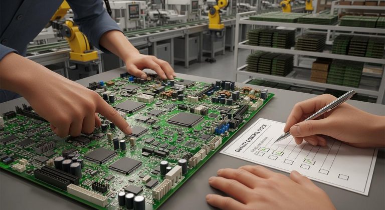
Testing and Quality Control
Testing and quality control ensure that the final pcbs meet industry standards. Various protocols validate the performance and reliability of the boards. For instance:
| Testing Protocol | Description |
|---|---|
| DFM (Design for manufacturability) | Ensures the board design is manufacturable, adhering to quality and cost guidelines. |
| Automated Optical Inspection (AOI) | Uses high-resolution cameras and laser scanners for automated comparison of pcb images. |
| Time Domain Reflectometer (TDR) | Measures characteristic impedance and checks for electrical discontinuities in pcb traces. |
| Flying Probe Test | A cost-effective in-circuit test for prototypes, using movable test probes based on software input. |
| First Article Inspection (FAI) | Validates that all required standards are met for the first manufactured circuit board. |
These testing methods identify defects early, ensuring the multilayer pcbs deliver consistent performance. Automated systems like AOI and TDR enhance accuracy and reduce human error, making them indispensable in modern manufacturing.
Tip: Collaborate with experienced manufacturers to ensure your pcbs undergo rigorous testing and meet all quality benchmarks.
Multilayer PCBs redefine efficiency and innovation in modern technology. Their compact structure and stacked layers enable high-density circuits, making them indispensable for industries like automotive, telecommunications, and consumer electronics. These PCBs excel in applications requiring complex traces and high-speed performance, such as battery management systems in electric vehicles and advanced communication devices.
The market for multilayer PCBs continues to grow, with projections showing steady expansion. For instance:
| Year | Market Size (USD Million) | CAGR (%) |
|---|---|---|
| 2024 | 24.9 | N/A |
| 2025 | 25.38 | N/A |
| 2033 | 26.35 | 1.9 |
Their lightweight and flexible design further enhance their versatility, supporting intricate functions like cell monitoring and thermal management. Despite challenges like higher costs and longer manufacturing times, the benefits of multilayer PCBs far outweigh the drawbacks. Their ability to handle complex circuits ensures they remain a cornerstone of technological advancement.
Note: As industries demand smaller, faster, and more reliable devices, multilayer PCBs will continue to play a pivotal role in shaping the future of electronics.
FAQ
What is the maximum number of layers a multilayer PCB can have?
The number of layers in a multilayer PCB depends on the application and manufacturing capabilities. Most designs range from 4 to 12 layers, but advanced applications, like aerospace systems, can exceed 50 layers. Consult your manufacturer for specific limitations.
How do you ensure signal integrity in multilayer PCBs?
You can ensure signal integrity by using proper layer stackup, controlled impedance, and dedicated ground planes. Minimizing crosstalk and electromagnetic interference (EMI) through careful routing also plays a critical role. Advanced simulation tools help validate designs before manufacturing.
Are multilayer PCBs suitable for flexible designs?
Yes, multilayer PCBs can be manufactured as rigid-flex boards. These combine rigid and flexible layers, allowing you to design compact, foldable circuits. They are ideal for wearable devices, medical instruments, and other applications requiring flexibility and durability.
How do you choose materials for multilayer PCBs?
Material selection depends on your application. High-frequency circuits require low-loss dielectrics, while automotive or aerospace systems need materials with high thermal resistance. Collaborate with your PCB fabricator to select materials that meet your performance and environmental requirements.
Can multilayer PCBs be recycled?
Recycling multilayer PCBs is challenging due to their complex structure and material composition. Specialized processes recover valuable metals like copper and gold. However, designing for sustainability and reducing waste during manufacturing can minimize environmental impact.
Tip: Partner with eco-conscious manufacturers to explore sustainable PCB options.