
 English
 Arabic
 Chinese (Simplified)
 Dutch
Dutch French
 German
 Italian
 Portuguese
 Russian
 Spanish
Why does pcb thermal management feel so tricky?
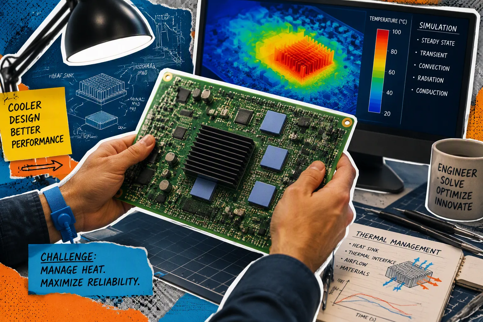
PCB thermal management feels tricky because it makes you carefully balance materials, shapes, and system limits that often work against each other. Getting heat out of a packed board is like trying to drain a clogged sink while someone keeps adding more dishes. This balance is a key problem in PCB design. For example, FR4 insulates electricity very well but does not move heat well. Metal core PCBs need special layers to block electricity and prevent shorts, which is a trade-off. Ceramic materials move heat 20–100 times better than FR4 while still insulating electricity, but their high cost limits their use. This post explains the physics, common mistakes, and practical tips for better heat control.
Key Takeaways
- Balance materials and shapes to move heat away from hot parts.
- Use copper pours and thermal vias to spread heat and reduce temperatures.
- Keep tall parts away from other components to avoid airflow shadows.
- Pick passive cooling for low power, and active cooling for high power.
- Test early models and run simulations early to make thermal management an easier job.
The Physics Behind PCB Thermal Management
Why Heat Paths Are Never Straightforward
Heat leaves a component through a chain of thermal resistances. Each link in that chain slows the flow, much like a narrow pipe restricts water. The die-to-package interface, the solder joint, the copper pad, the dielectric layer, and the surrounding air all add resistance. Engineers call this stack the thermal resistance path. A weak link anywhere in the chain limits the whole system.
Copper thickness matters a lot here. Thin copper foil carries less heat sideways, so heat builds up near the source. Thick copper spreads heat over a wider area and lowers the local temperature. Designers often choose heavy copper layers for this reason. The dielectric material also plays a role. FR4 does not conduct heat well, so most heat must travel through copper instead of through the board itself.
Heat paths bend, split, and merge. A via array under a power device gives a vertical route to inner copper planes. Those planes then spread heat sideways. If the planes are broken into pieces, the path narrows and thermal resistance rises. A continuous ground plane usually works far better than several small islands.
Balanced copper distribution keeps temperatures even across the board. A study showed that a 20% difference in copper density across a PCB can cause temperature variations of up to 10°C in high power applications. Balancing copper distribution reduces these temperature gradients, directly supporting how well balanced copper reduces thermal unevenness.
How Power Density Creates Hot Spots
Modern components pack more power into smaller footprints. A tiny die can dissipate several watts across a few square millimeters. That concentration creates a hot spot, a small region much hotter than the rest of the board. Hot spots speed up aging, shift component values, and eventually cause failures.
Real designs show this pattern again and again. The table below summarizes documented cases.
| Case Study | Design / Power Context | Hot Spot Formation Mechanism | Impact on Component Reliability | Mitigation / Outcome |
|---|---|---|---|---|
| Sealed offshore electronics enclosure | Sealed passive enclosure; submerged seawater at 30°C and outdoor air at 40°C; target component temperature below 60°C | Weak natural convection and poor internal conduction to enclosure walls; hot spot spreading resistance significantly contributed to overall temperature rise | Passive design was insufficient for the outdoor air case, creating risk that components would exceed the 60°C limit | Recommended increased external surface area with fins or bonded heat sink, improved internal conduction and reduced interface resistance, and heat pipes or vapor chambers to reduce spreading resistance |
| Multi-cold-plate liquid cooling system for EV battery | 4 kW liquid cooling system with four cold plates, heat exchanger, DC-DC converter, and onboard charger | Thermal performance needed balancing with manufacturability and flow distribution; localized heat concentration risk in cold plate and loop design | Ineffective kilowatt-scale cooling could lead to thermal stress and reduced reliability of EV battery and power electronics | Optimized cold plate geometry and system flow; 10-pass serpentine tube design maximized heat transfer while maintaining acceptable pressure drop and manufacturability |
| Ruggedized rack system | Sealed 241 W ruggedized rack with 55°C ambient limit | Baseline CFD identified thermal violations; airflow inefficiencies and heat sink limitations created hot spot risks | Thermal violations threatened component reliability before failure; sealed systems required holistic optimization | Revised heat pipe routing, heat sink replacement, fan reconfiguration, and removal of airflow obstructions; all components achieved thermal compliance |
| Passive aluminum enclosure | Sealed passive aluminum enclosure dissipating 75.8 W at 25°C ambient | Interface resistance and restricted airflow limited passive cooling; internal conduction and external convection interaction governed performance | Thermal constraints could prevent target performance and increase component temperatures | Improved thermal interface materials, better heat spreading, optimized fin geometry, reduced obstructions, and added vent gaps to enhance natural convection pathways |
| 150 kW fast-charge cabinet retrofit | 150 kW fast-charge cabinet; axial fans switched to EC centrifugal blower | Peak-load thermal buildup risk; service filter pressure drop increase of 40% could reduce flow and cause hot spots | Thermal derating and repeated warranty returns were prevented | Field validation showed inlet temperature reduction of 8°C under peak load and about 30% fan power reduction while maintaining flow |
A 150 kW fast-charge cabinet was retrofitted from axial fans to an EC centrifugal blower. Field validation demonstrated an inlet temperature reduction of 8°C under peak load and approximately 30% lower fan power, while maintaining airflow even when a service filter increased pressure drop by 40%. This thermal management change prevented thermal derating and avoided repeated warranty returns, directly linking hot-spot/thermal control in a high-power-density design to improved component reliability.
These cases share a lesson. Hot spots form where heat generation outpaces local heat dissipation. Spreading resistance, interface resistance, and blocked airflow all make the problem worse. Designers who address these factors early avoid expensive redesigns later.
Common Thermal Management Pitfalls
Ignoring Via Thermal Resistance
A via is a copper tube. Many designers think it works like a perfect heat pipe. That idea fails in real boards. Each via adds its own thermal resistance to the heat path. Plating thickness, drill diameter, and via length all affect that resistance. Thin plating or a long barrel slows heat flow. The heat path then gets stuck at the via group. This bottleneck raises the temperature of the part above it.
Engineers often put just a few vias under a power device and call it done. A small group can only move limited heat. Heat crowds into those few barrels. The local temperature rises. The fix needs more vias, wider barrels, or thicker plating. Each choice affects routing space and cost. Ignoring this detail hurts the whole thermal plan. A careful PCB design review finds this error before production. Good PCB thermal management starts with this knowledge.
Symmetrical Spreading and Air Flow Shadows
Heat does not spread in a perfect circle. Designers sometimes think it spreads evenly around a hot part. Real boards break that symmetry. Copper planes end. Traces make narrow paths. Nearby parts block the way. One side of a device can run much hotter than the other. This uneven heat stresses solder joints and shortens their life. High power designs suffer most from this effect. Balancing copper across the board reduces these differences.
Airflow is another trap. A tall part creates an air flow shadow. Parts behind it sit in still air. They overheat even when the fan moves plenty of air. Increasing space between traces helps spread heat. But small PCBs rarely allow that. Designers then must use other thermal methods. A thermal simulation that ignores these shadows gives false trust. Map airflow paths early in the layout process.
A common mistake is trusting a simulation that shows even heat but ignores real air flow shadows and gaps in copper.
Practical Thermal Management Strategies
Copper Pours, Thermal Vias, and Trace Spacing
Copper pours give heat a wide path to flow. A big copper area under a hot part spreads heat to the sides and lowers the local temperature. Designers join these pours to inner layers using thermal vias. Each via acts like a small vertical tube. A group of vias moves much more heat than one barrel. AllPCB’s guide says filled thermal vias under a thermal pad on boards thicker than 0.7 mm can cut thermal resistance by up to 20%. That cut matters in high power uses where every degree counts.
Trace spacing also affects heat flow. Wider spacing between traces spreads heat over a larger area. Small boards often lack that space. Designers then use copper pours and via arrays instead. A solid ground plane works better than many small islands because it moves heat without breaks. This method forms the backbone of good PCB thermal management.
Heatsinks, Enclosures, and Placement
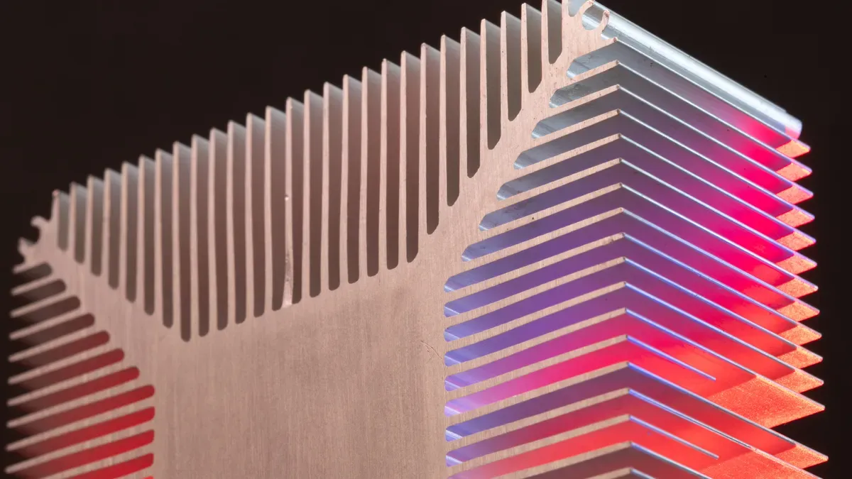
A heatsink draws heat off the part’s surface. Thermal pillars and thick pads fill the space between the part and the sink. These parts lower resistance at the connection. Active cooling adds fans or pumps when passive ways are not enough. The table below compares these two options.
| Cost-Effectiveness Factor | Passive Cooling | Active Cooling |
|---|---|---|
| Bill-of-materials cost | Lower (no fans, pumps, or TECs) | Higher (fans, pumps, TECs, mounting hardware) |
| Assembly complexity | Minimal; simple heatsink or copper pour | Increased; requires wiring, ducting, placement |
| Power draw | None (zero operating cost) | Consumes power for fans or pumps |
| Reliability and maintenance | High (no moving parts) | Lower MTBF due to wear parts |
Where you place parts decides how well heat leaves. A tall part creates an airflow shadow. Parts behind it stay in still air and get too hot. Designers line up parts with vent paths so air reaches every hot spot. A case that conducts heat spreads it through its walls. Thermal relief patterns balance heat flow when soldering. These patterns slow heat loss at pad connections, keeping solder joints clean.
Every choice here affects how well heat moves. A copper pour costs little and uses no power. A fan moves more heat but adds noise, cost, and parts that wear out. Engineers balance these factors with space and money. Good thermal plans mix passive and active methods only when needed. This balance keeps PCB design practical and reliable.
Thermal Management Trade-offs and Decisions
Cost, Space, and Manufacturability
Every thermal choice comes with a cost. Designers must balance cost, space, and how easy something is to build. A copper pour is cheap and adds no extra parts. A fan moves more heat but brings noise, uses power, and can wear out. Small devices have the tightest limits. Via-in-pad thermal vias put heat paths right under a component. They save board space because they need no extra room. But adding too many vias can make the board weaker or block routing on other layers. Designers must plan carefully so they do not hurt the overall pcb design.
Real examples show this balance. A high-power LED module might use a QFN package with 10–15 via-in-pad thermal vias. These vias carry heat to a bottom copper layer and keep the LED junction below 100°C at 5W or more. A smartphone processor might use 20 microvias at 0.1 mm diameter to send heat to an internal ground plane. This keeps temperatures safe during heavy use without making the footprint bigger. Each added via raises manufacturing cost and complexity. Engineers must decide when the thermal gain is worth the expense.
A Decision Framework
A simple framework helps you pick the right thermal management strategies. First, set the design goal. Is the limit a junction temperature, a surface temperature, or a cost target? Second, list the constraints. Space, budget, and assembly methods all narrow your options. Third, match the technique to the goal. Passive methods like copper pours and thermal vias work well for low-cost, low-power boards. Active cooling works for high power applications where passive methods are not enough.
Heat sink geometry also matters. The table below shows how each parameter affects cooling.
| Parameter | Function | Impact on Cooling |
|---|---|---|
| Height | Increases total surface area | Can block air in tight spaces |
| Thickness | Conducts heat upwards | Adds weight and material cost |
| Pitch | Airflow channel width | Balances pressure drop |
| Profile | Shape optimization | Affects turbulence creation |
Flared fins work when vertical clearance is tight but horizontal space is ample. Plate fins suit linear airflow. Pin fins offer omnidirectional air entry. Thermal analysis through simulation and testing must confirm every choice. A design that looks good on paper can fail in real air. Engineers should simulate early, test prototypes, and iterate as constraints become clear. This approach turns thermal management from guesswork into a manageable task.
Tricky does not mean impossible. A systematic approach turns thermal management from a guessing game into a manageable engineering task. Early simulation reveals heat paths before layout freezes. Awareness of trade-offs guides every choice.
Readers should start with the decision framework. They can select thermal management strategies that match their design goals. They then iterate as constraints become clearer. This method works for low-power boards and high power applications alike. Each pass through the framework sharpens the thermal picture. Engineers who test prototypes and refine their assumptions build reliable products. The physics stays complex, but the process stays under control.
FAQ
Why does FR4 make heat removal harder?
FR4 is good at stopping electricity but bad at moving heat. Heat has to move through copper instead of the board. Designers add copper pours, planes, and thermal vias to give heat a better path. Without those, heat builds up near the source and makes local temperatures higher.
Do more thermal vias always lower temperatures?
No. Each via has its own resistance to heat flow. Plating thickness, drill size, and barrel length limit how much heat a via moves. A small group of vias can create a bottleneck. More vias help, but space and cost set real limits.
Why do airflow shadows matter so much?
A tall part blocks air from reaching parts behind it. Those parts sit in still air and get hotter, even when a fan moves plenty of air. Designers line up parts with vent paths so air reaches every hot spot. Simulation that ignores these shadows gives false confidence.
Can simulation alone confirm a thermal design?
No. Simulation helps early layout choices, but real air and real interfaces act differently. Engineers should simulate early, then test prototypes and refine assumptions. This step-by-step method turns thermal management from guesswork into a manageable task.