 English
 Arabic
 Chinese (Simplified)
 Dutch
Dutch French
 German
 Italian
 Portuguese
 Russian
 Spanish
How Does SMT PCB Assembly Help Create Smaller Devices?
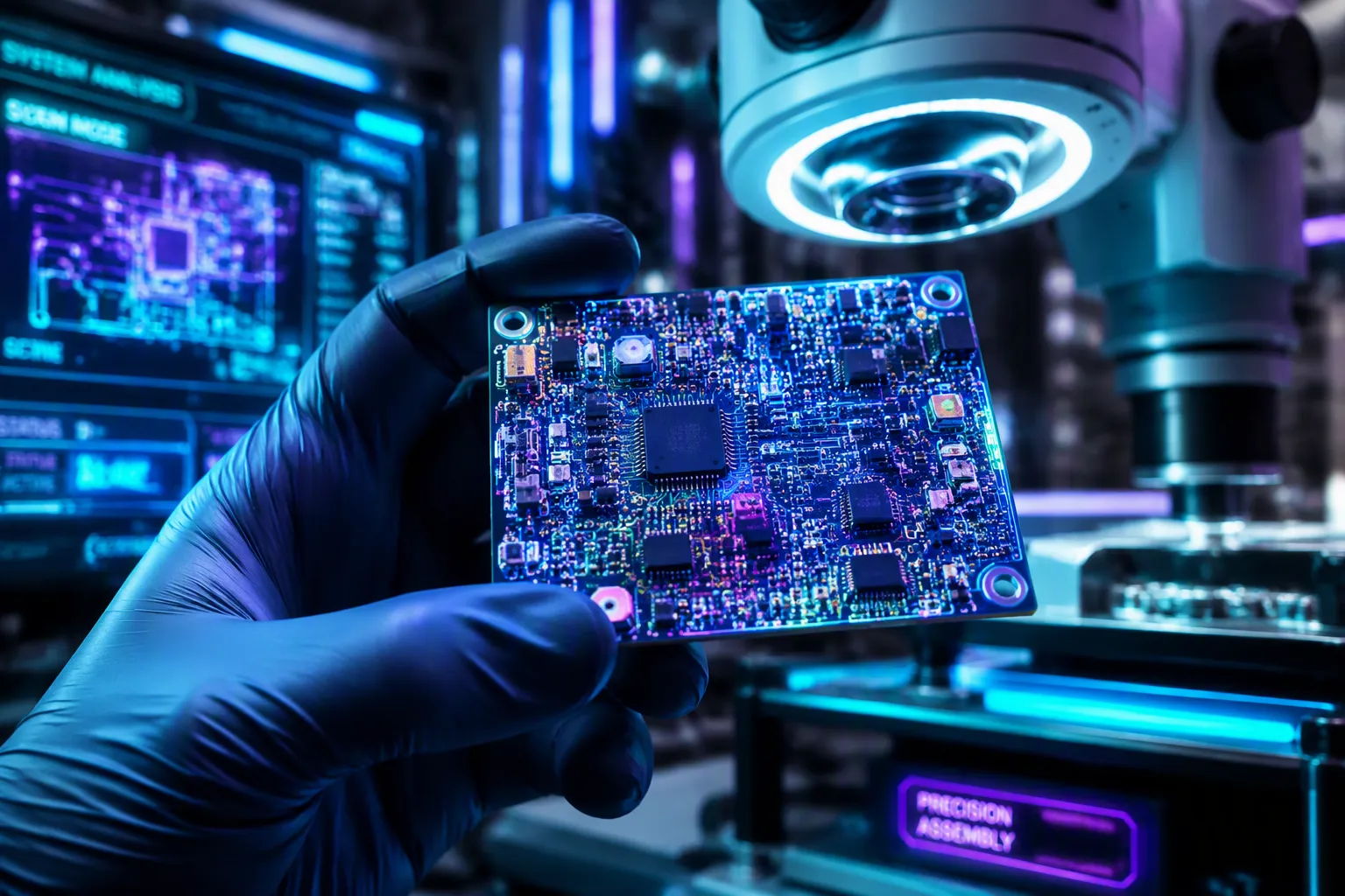
SMT PCB assembly helps make smaller devices by removing through-holes, using smaller surface-mount parts, and fitting more components in less space. Surface mount technology is a way to attach electronic parts right onto the surface of a printed circuit board. Older through-hole assembly needed holes drilled through the PCB and bulky parts with long leads. That process wasted useful space on every board. This process changed everything for modern electronics. You will learn each technical reason behind this change and see real devices that got smaller because of it. The process of SMT PCB assembly now powers almost every compact gadget you use today.
Key Takeaways
- SMT uses tiny parts that take up far less space than older through-hole parts.
- SMT gets rid of through-holes, which lets you use both sides of the board and saves space.
- SMT can fit up to 100 components per square inch, making devices smaller and more powerful.
- Smaller spacing and more pins let you add more features without making the board larger.
- Automated machines place very small parts with great accuracy, which allows them to make small, complicated devices.
How SMT PCB Assembly Shrinks Devices
SMT PCB Assembly vs. Through-Hole
Surface mount technology is a way to build circuit boards where you attach components right onto the PCB surface using machines. Through-hole assembly, the older method, makes you drill holes through the PCB and push component leads through them. This difference creates a huge gap in how small your final device can be.
One big difference shows up in component density. The table below compares how many components you can fit per square inch with each technique.
| Mounting Technique | Component Density per Square Inch |
|---|---|
| SMT | Up to 100 components |
| Through-Hole | Typically 10–20 components |
With SMT, you can fit five to ten times more parts in the same space. That directly makes your final product smaller.
The manufacturing process also differs a lot. SMT uses reflow soldering, which heats solder paste to attach components to the board surface. Through-hole assembly needs wave soldering or hand soldering on the other side after you insert leads. The whole pcb assembly process for SMT skips pre-drilled holes, so you can place components on both sides of the PCB. This doubles the space you can use. The automated pick-and-place process can position tiny parts like 0402 and 0201 packages with amazing precision. These small packages are common in medical wearables, compact industrial controllers, and portable electronics. Human hands could never reach this level of accuracy. The process depends on computer-controlled machines to place hundreds of components per minute.
The differences also show up in the final product. A PCBA made with SMT is lighter, smaller, and more reliable than one made with through-hole parts. You get a finished board that fits easily into tight enclosures.
Three Core Reasons for Miniaturization
SMT delivers smaller devices for three core reasons.
First, the components themselves are smaller. Surface-mount parts have short leads or no leads at all. They take up much less room than through-hole parts. Resistors and capacitors come in ultra-small sizes like 0402. You can fit many more components on a board without making the board bigger. Designers pick these tiny packages for compact devices like wireless earbuds and smartwatches.
Second, you get rid of through-holes. Drilling holes uses up precious PCB space and stops you from placing components in those spots. SMT frees that space completely. You can now use both sides of the board to place parts. This effectively doubles the available real estate. You can fit the same functionality on a board half the size.
Third, you get higher component density. As the table showed, SMT allows up to 100 components per square inch, compared to only 10–20 for through-hole. This high density means you can pack more features into a small area. You do not need to make your device larger just to add more functions. The circuit board assembly process for SMT makes this possible by supporting fine-pitch parts and small footprints.
Each reason builds on the others. Smaller parts, no wasted holes, and dense placement all work together. The result is a PCB that holds the same capability in a fraction of the space. This is why almost every modern compact gadget relies on SMT.
Smaller Components, Smaller Boards
Surface Mount vs. Through-Hole Parts
The size gap between surface-mount and through-hole parts is huge. Through-hole components have big bodies with long metal leads. Those leads must go through drilled holes in the pcb. They use up space on both sides of the board. Surface-mount parts are different because they have short leads or none at all. They sit right on the pcb surface. This one difference saves a lot of space on every board you design.
Think about a common through-hole axial resistor. It is a typical through-hole axial resistor with wire leads sticking out from each end. A matching surface-mount resistor in the 0603 package is only 0.06 by 0.03 inches. That is a huge drop in footprint. The same comparison works for capacitors, diodes, and integrated circuits. Every surface-mount component uses far less board space than its through-hole equivalent.
The history of component sizes shows this clearly. Through-hole technology ruled from the late 1950s through the 1970s. The early 1980s brought a mixed-technology phase that combined both methods. From the 1990s onward, the surface-mount age took over fully with tiny, lead-less packages. Today the smallest standardized SMD package is the 01005, measuring just 0.4 mm by 0.2 mm. You find these tiny components inside smartphones, wearables, and medical electronics. This size reduction directly makes your device’s compact form possible.
Why Smaller Parts Matter
Smaller components lead straight to smaller boards and smaller devices. Swapping through-hole parts for surface-mount parts can shrink your pcb size by about 60 to 70 percent. Think about what that means for your product. You fit the same circuit into a fraction of the space.
This shrinkage opens new possibilities. With smaller parts, you get higher component density on your board. More components fit into every square inch. You can also place parts on both sides of the pcb. This doubles the area you have for component placement. Double-sided component placement gives you a key advantage over through-hole technology. Its leads already use up space on both sides.
The result changes what you can build. A device that once needed a large enclosure now fits in your pocket or on your wrist. The ongoing miniaturization of electronic components pushes this trend forward. Each generation of smaller resistors, capacitors, and integrated circuits lets you pack more functionality into the same device volume.
No Holes, No Wasted Space
How Through-Holes Consumed Board Area
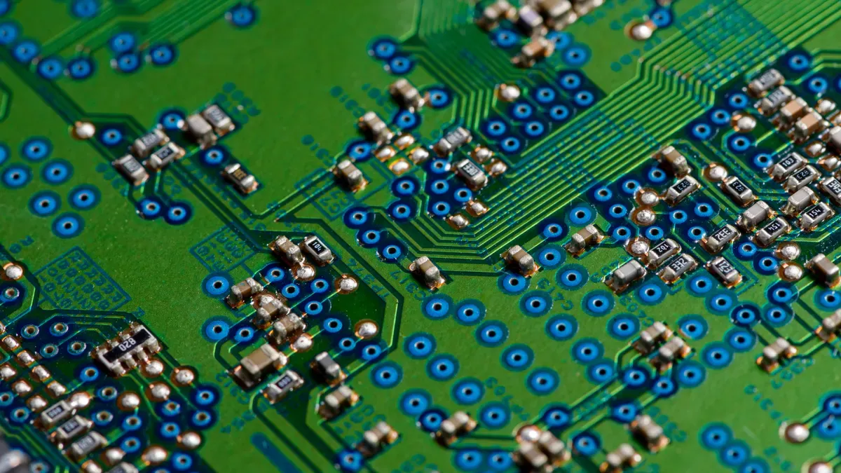
Through-hole assembly made you drill a hole through the whole pcb for each component lead. Every hole took up room on the top layer and the bottom layer at once. You could not put any part on that hole or right under it. The drill also needed a keep-out zone around it, so the wasted space was even bigger than the hole. A board with hundreds of through-holes lost a lot of usable surface to empty rings and clearance zones.
This problem got worse as your design added more parts. Each new through-hole component needed its own drilled hole and its own keep-out area. The board had to grow bigger just to hold the holes, not the electronics. That is why older devices were so bulky. The pcb itself was mostly empty space around drill points.
Using Both Sides of the Board
SMT changes this fully. You mount components right onto the surface, so no holes are needed. Both the top and bottom layers become fully open for placement. This doubles your usable area without making the board any bigger. Double-sided SMT assembly places and solders parts on both faces of the pcb, which supports much more complex and compact designs.
The results show it clearly. A PCBGOGO customer making smart wristbands started with single-sided SMT. That approach needed tightly packed parts and an extra interposer board, which raised cost and power use. After moving several components to the bottom layer with double-sided SMT, the pcb area shrank by 30 percent. The product thickness dropped by 2 mm, and battery life improved by 15 percent.
Double-sided placement also opens design choices that single-sided boards cannot offer. You can keep RF sections away from noisy digital circuits by placing them on opposite faces. Shorter trace routing between layers improves signal integrity. You can also separate heat-sensitive parts from heat-generating ones. Electric vehicle battery monitoring systems use SMT boards that pack more than 100 components per square inch. That density delivers greater sensor coverage and smarter power management without added bulk or weight.
Finer Pitch, More Function
What Pin Count and Pitch Mean
Pin count is simply the number of electrical connections a component has. A tiny resistor might have two pins. A smartphone processor can have several hundred. Pitch is the distance from the center of one pin to the center of the next pin. You measure it in millimeters.
Common pitch ranges vary from standard values to very fine pitches for high-density components. For example, standard packages like QFPs and SOICs use typical pitches, while fine-pitch packages like small-outline packages or BGAs use finer pitches. As pitch shrinks, you can fit more connections into the same package footprint.
A higher pin count means the chip can do more work. But adding pins forces you to reduce pitch. That is where the trade-off lives. As pitch shrinks, you fit more connections into the same package footprint.
This relationship drives miniaturization. Each step down in pitch unlocks more capability. It also raises assembly difficulty. At standard pitches, placement works fine. At very fine pitches, you need specialized stencils and tighter process controls.
Packing More Into Less Space
Finer pitch and higher pin count let you pack more functionality into your pcb. A QFP package with a fine lead spacing holds many more pins than a coarser version of the same body size. Smartphone processors use these fine-pitch packages to maximize connections in very limited board space.
The result is impressive. Higher pin counts support devices that need greater processing power. Microprocessors and system-on-chip designs rely on this density. You get more computing power in a package that sits on your fingertip.
This capability demands advanced circuit board methods. HDI technology supports fine-pitch BGAs and high-pin-count ICs. It lets designers integrate new features without making your device bigger. You can pack more components into the same board area.
However, finer pitch raises precision demands across every assembly step. At very fine pitches, the gap between leads becomes very small. Solder paste printing needs careful control. Placement machines must align each part with high accuracy. The payoff is worth it. You get far greater performance from the same small pcb space. Two sides of the board. No wasted real estate from holes. Just dense, capable electronics that fit in your pocket.
Precision Placement by Automation
Solder Paste, Pick-and-Place, Reflow
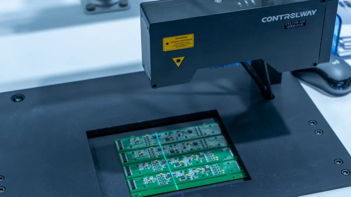
The pcb assembly process starts with solder paste printing. A stencil deposits solder paste onto the pads where components will sit. This step matters because the paste must hold parts in place and form strong joints during reflow. Smaller pads and finer pitch parts need thinner stencils and tighter aperture tolerances. Any excess paste can cause bridges, and too little paste leads to weak connections.
Next comes component placement. Pick-and-place machines use fine-tuned nozzles and vacuum mechanisms to lift and position parts onto the pcb. Placement precision is critical because smaller components and dense layouts leave no room for error. Even slight misalignment can cause shorts, opens, or tombstoning. After placement, the board moves through a reflow oven. The solder paste melts and then solidifies to form electrical connections. The reflow temperature profile must be precise. You need enough heat for complete reflow, but not so much that sensitive parts get damaged. For miniaturized assemblies, tighter process control prevents voids, solder bridges, and component damage.
Why Automation Is Essential
Human hands could never place parts this small with this accuracy. Modern pick-and-place machines achieve high placement accuracies through vision system alignment and regular calibration. High-speed pick-and-place machines can reach very high component placement rates with excellent accuracy. These systems use high-resolution cameras and precision servo motors to handle 01005 resistors measuring just 0.4 mm by 0.2 mm.
A typical SMT design needs a placement tolerance tight enough to ensure proper soldering. Automated lines deliver this repeatability at speeds no manual process can match. The automated nature of SMT assembly also lowers labor costs and reduces human error. This improves product quality and consistency across batches. After soldering, automated optical inspection scans the board for misplaced parts or solder bridges. X-ray inspection checks hidden connections on BGAs and QFNs. Each step in the process builds on the last. Precision at every stage determines how far miniaturization can go without sacrificing yield or reliability.
Real Devices Made Possible by SMT
Smartphones, Wearables, and Earbuds
Think about the smartphone in your pocket. It has a fast processor, several cameras, and wireless radios inside a thin case. None of this works without SMT. Every smartphone uses a complex pcb covered in tiny surface-mount components. The processor, memory chips, and power management circuits all sit on that board. Without SMT, your phone would be as thick as a brick.
Wireless earbuds show this even more clearly. Each bud holds a Bluetooth chip, battery, microphone, speaker driver, and touch sensors. All these parts fit inside a case smaller than your fingertip. Through-hole parts could never fit this many components. The pcb inside each earbud holds dozens of surface-mount parts on both sides. That is why your earbuds feel almost weightless in your ears.
Fitness trackers and smart rings work the same way. These devices must sense your heart rate, count your steps, and talk to your phone. All that power comes from a tiny board packed with sensors and processors. SMT makes these products possible by letting makers shrink the board while keeping every feature.
Smartwatches, Fitness Trackers, and Medical Wearables
Smartwatches push miniaturization even further. A modern smartwatch has a color touchscreen, GPS receiver, heart rate monitor, accelerometer, gyroscope, barometer, and wireless charging coils. Every single function depends on surface-mount components placed with automated precision. The result is a full computer on your wrist that lasts all day on a small battery.
Medical wearables save lives through this same technology. Hearing aids now fit completely inside your ear canal. Continuous glucose monitors stick to your arm and send data wirelessly. Implantable pacemakers watch your heart from inside your chest. Each device uses SMT to pack critical electronics into the tightest possible space. The board inside a modern hearing aid is extremely small. It holds dozens of components that process sound in real time without any delay.
What makes all these devices work is one shared technology. Smaller parts sit on both sides of the pcb. Dense placement packs more function into less space. Automated assembly places every tiny part with precision. The gadgets you use every day prove that SMT changes what electronics can achieve.
SMT PCB assembly is the main reason today’s small electronics exist, not just another option. Smaller parts, no through-holes, higher density, finer pitch, and automated precision all push this change. Your smartphone, earbuds, and smartwatch show it works. The circuit board assembly process fits more function into less space. Looking ahead, miniaturization will keep going with flexible, stretchable, and wearable designs. The demand for miniaturized circuit board assembly will continue to expand. Medical devices and IoT will push even further. The pcb assembly process will keep improving quality and testing. Reflow, reflow, reflow, reflow, reflow, reflow, reflow. Testing, testing, testing, testing, testing. Process, process, process, process, process. Quality, quality, quality. Pcb, pcb, pcb.
FAQ
How much smaller can SMT make a circuit board?
You can shrink a pcb by about 60 to 70 percent when you swap through-hole parts for surface-mount parts. Double-sided placement doubles your usable area. Finer pitch and higher pin counts pack more function into the same footprint. The process keeps improving every year.
Why can’t you use human hands to place SMT components?
Modern pick-and-place machines reach high placement accuracies. They handle 01005 resistors measuring just 0.4 mm by 0.2 mm. High-speed systems place components at very high rates. Human hands could never match this precision or speed. The process depends on automation.
What role does testing play in SMT assembly?
Testing catches misplaced parts and solder bridges after reflow. Automated optical inspection scans every board. X-ray inspection checks hidden connections on BGAs and QFNs. This testing protects quality and keeps your yield high. Each testing step builds on the last.
Does SMT work for both sides of a PCB?
Yes. SMT lets you mount components on the top and bottom layers. No through-holes block either side. This doubles your usable board area without making the pcb bigger. Double-sided assembly supports complex, compact designs. The process handles both faces with equal precision.
What everyday devices rely on SMT?
Your smartphone, wireless earbuds, and smartwatch all depend on SMT. Hearing aids, fitness trackers, and continuous glucose monitors use it too. These devices pack processors, sensors, and batteries into tiny spaces. Testing ensures each one works reliably. The process makes modern wearables possible.