What is PCB Cloning and How It Shapes Modern Electronics
PCB cloning, or PCB Clone, refers to the process of duplicating an existing printed circuit board design, including its layout, components, and connections. This technique plays a pivotal role in modern electronics by enabling you to replicate successful designs efficiently. It can significantly reduce costs associated with maintaining legacy systems, allowing companies to avoid expensive upgrades. By copying existing designs instead of starting from scratch, you save time and resources. Additionally, PCB cloning facilitates design optimization, leading to cost-effective manufacturing and faster time-to-market for new products. These benefits make PCB Clone a cornerstone for innovation and product development in the electronics industry.
Key Takeaways
- PCB cloning helps copy circuit board designs, saving time and money.
- It lowers costs by cutting prototype expenses and speeds up product launches.
- Cloning lets you change and improve designs to fit specific needs.
- Always follow ethical rules in cloning to avoid breaking laws.
- PCB cloning is important for electronics and medical tools, boosting innovation.
Understanding PCB Cloning
What is PCB Cloning?
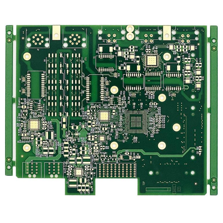
PCB cloning refers to the process of replicating an existing printed circuit board design, including its layout, components, and connections. This technique involves reverse engineering a PCB to extract its design files, such as the Gerber file, bill of materials (BOM), and schematics. By doing so, you can reproduce the board with high precision, ensuring it functions identically to the original.
The cloning process typically includes several steps, such as extracting the integrated circuit (IC) program, reverse engineering the PCB, building prototypes, and testing the final product. The table below outlines these steps in detail:
| Step | Description | Completion Percentage |
|---|---|---|
| IC Unlock | Extract the IC program | 25% |
| PCB Reverse Engineering | Get Gerber file, BOM list & Schematics From PCB Sample | 50% |
| PCB Prototype | Build New Boards By Using the Extract IC Program & PCB Files | 75% |
| Testing & Debug | Check the Function of the New Board, Fix incompatibility & Debug other errors. Update New Corrections into PCB files | 100% |
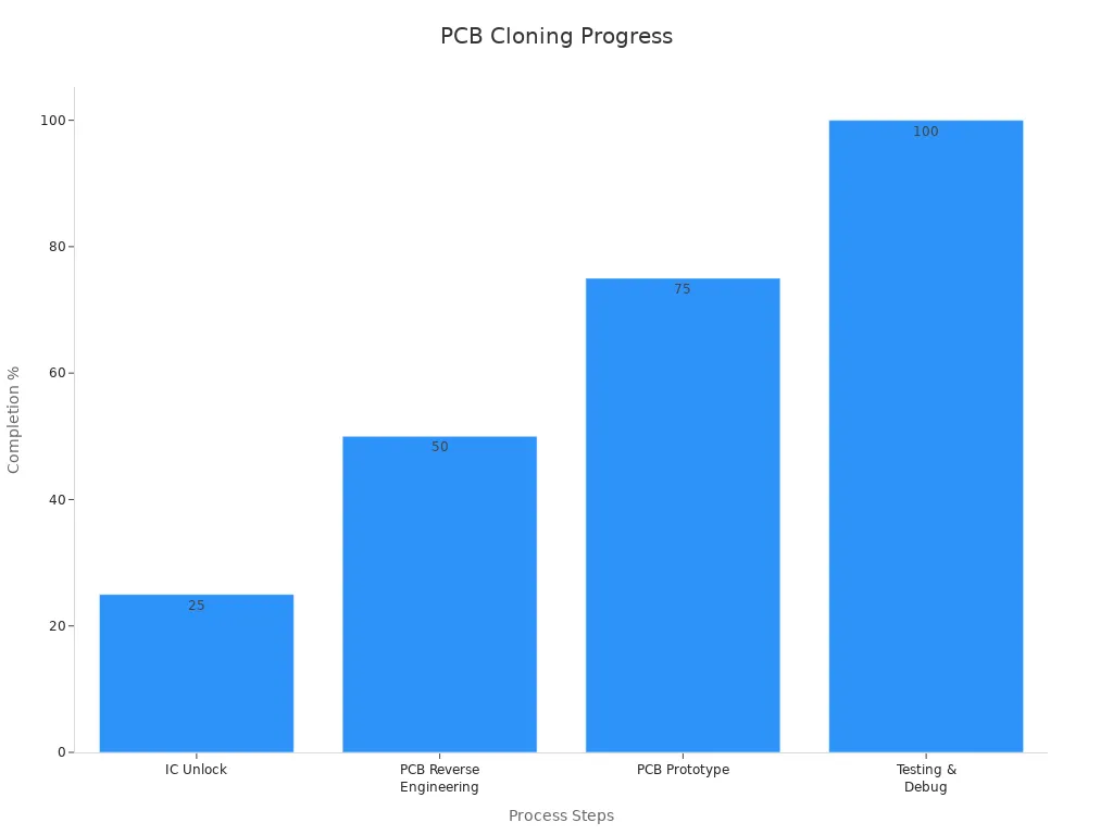
This structured approach ensures that the cloned PCB meets the required specifications and performs reliably in its intended application.
Why is PCB Cloning Important?
PCB cloning plays a crucial role in modern electronics by addressing several industry challenges. It enables you to replicate existing designs, saving time and resources that would otherwise be spent on creating new layouts from scratch. This is particularly valuable when dealing with legacy systems or obsolete components, where original design files may no longer be available.
The demand for efficient and reliable printed circuit boards (PCBs) is increasing across various industries, particularly due to the growing adoption of Internet of Things (IoT) devices.
Cloning also supports cost-effective manufacturing by reducing prototyping expenses and accelerating time-to-market. For example, companies can quickly produce prototypes for testing and validation, ensuring faster product launches. Additionally, it allows for design optimization, enabling engineers to modify and improve existing designs without starting over.
As the global market for electronic devices continues to expand, the need for high-quality PCBs has become more critical than ever.
By leveraging PCB cloning, you can stay competitive in a fast-paced industry while meeting the growing demand for innovative and reliable electronic devices.
Common Misconceptions About PCB Cloning
Despite its benefits, PCB cloning is often misunderstood. One common misconception is that cloning is synonymous with intellectual property theft. While unethical cloning practices exist, legitimate cloning focuses on reverse engineering for innovation, repair, or optimization purposes. When done ethically and within legal boundaries, cloning can drive technological advancements and reduce costs.
Another misconception is that cloning compromises quality. In reality, modern cloning techniques use advanced imaging tools and software to ensure high precision and reliability. For instance:
The market for cloned electronics is expanding, driven by sophisticated imaging tools and the rise of contract manufacturing, which allows for easier exploitation of design files by cloners.
Some also believe that cloning is only useful for copying outdated designs. However, it is widely used in cutting-edge industries, including medical equipment, consumer electronics, communication devices, and industrial control systems. This versatility makes it a valuable tool for both legacy and modern applications.
By understanding these misconceptions, you can better appreciate the potential of PCB cloning as a legitimate and innovative practice in electronics design and manufacturing.
The Process of PCB Cloning
Reverse Engineering the PCB
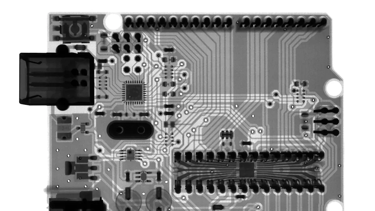
Reverse engineering the PCB is the first and most critical step in the pcb cloning process. This involves analyzing the existing circuit board design to understand its layout, components, and connections. You begin by scanning the pcb using advanced imaging tools to capture details like component placement and routing. This step ensures that every element of the board is accurately documented.
The process also includes intellectual property verification. By reverse engineering the pcb, you can confirm compliance with legal standards and resolve potential disputes. This stage lays the foundation for creating a cloned pcb that matches the original in both functionality and design.
| Stage | Description |
|---|---|
| Intellectual Property | Verification of intellectual property rights through reverse engineering to support legal disputes. |
| PCB Scanning | Scanning the circuit board to capture details like component placement and routing. |
| Reverse Analysis | Analyzing components and circuit routing from the scanned PCB to ensure accuracy. |
| Generate Files | Creating engineering files using CAD tools, including Gerber, PDF, and schematic diagrams. |
| PCB Clone/Copy | Cloning existing PCBs to reproduce an exact copy of the board. |
Extracting the Circuit Design
Once the reverse engineering phase is complete, the next step is extracting the circuit design. This involves generating essential engineering files such as Gerber files, schematic diagrams, and the bill of materials (BOM). These files serve as the blueprint for the cloned pcb, ensuring that every detail of the original design is replicated.
During this stage, precision is crucial. Errors in extracting data can lead to functional issues in the final product. For example, IC unlocking has an error rate of 25%, while reverse engineering the pcb has a 50% error rate. Advanced tools and techniques help minimize these errors, ensuring the cloned pcb meets the required specifications.

Reproducing the PCB Design
The final step in the pcb cloning process is reproducing the pcb design. Using the extracted files, you can create an exact replica of the original circuit board. This involves manufacturing the board, assembling the components, and testing the final product to ensure it functions as intended.
Testing and debugging play a vital role in this stage. Any incompatibilities or errors identified during testing are corrected, and the updated design is incorporated into the final files. This iterative process ensures that the cloned pcb is reliable and ready for deployment.
By following these steps, you can successfully complete the pcb cloning process, creating a high-quality replica that meets your specific needs.
Testing the Cloned PCB
Testing the cloned PCB is a critical step in ensuring its functionality and reliability. After completing the reverse engineering and reproduction phases, you must validate the board’s performance through rigorous testing procedures. This step guarantees that the cloned PCB matches the original design and operates as intended.
Several testing methods are commonly used to verify the functionality of cloned PCBs. Each method targets specific aspects of the board’s design and performance:
| Testing Method | Description |
|---|---|
| In-Circuit Testing (ICT) | Activates and powers individual components on the PCB, providing high coverage rates (85-90% common). |
| Automated Optical Inspection | Uses 2D or 3D cameras to capture images of the PCB, comparing them to a schematic to identify deviations for further inspection. |
| Functional Testing | Validates the product’s functionality using external equipment and ensures compliance with industry standards. Though effective, this method can be time-consuming. |
In-circuit testing (ICT) is particularly effective for identifying issues at the component level. It ensures that each element of the cloned PCB functions correctly within the circuit. Automated optical inspection (AOI) complements ICT by visually analyzing the board for defects such as soldering errors or misaligned components. Functional testing evaluates the overall performance of the board, ensuring it meets the intended application requirements.
Testing also involves debugging and refining the cloned PCB. Any discrepancies or errors discovered during testing must be addressed promptly. For example, if a component fails to activate during ICT, you may need to revisit the reverse engineering process to identify the root cause. This iterative approach ensures successful PCB cloning and prepares the board for deployment in real-world applications.
By employing these testing methods, you can achieve high reliability and precision in your cloned PCB. Testing not only validates the cloning process but also enhances the board’s quality, ensuring it meets industry standards and customer expectations.
Applications of PCB Cloning in Modern Electronics
Prototyping and Product Development
PCB cloning plays a vital role in prototyping and product development. When you replicate an existing electronic product, you can bypass the lengthy design phase and focus on refining the prototype. This process accelerates time to market, allowing you to test and validate designs faster. By leveraging PCB clone prototype services, you gain access to proven layouts and components, reducing the risk of errors during development.
The role of PCB cloning in PCB redesign and development extends beyond replication. It enables you to develop a PCB with alterations tailored to specific requirements. For instance, you can modify existing designs to improve performance or integrate new features. This flexibility makes cloning indispensable for creating innovative products that meet evolving market demands.
| Benefit/Application | Description |
|---|---|
| Reduced time to market | Shortens the product development process by enabling the reuse of proven designs. |
| Customization of designs | Allows companies to modify existing designs or create unique products tailored to specific needs. |
| Streamlined processes | Helps streamline manufacturing processes, saving time and money. |
By utilizing PCB clone services, you can mass produce multiple PCB copies for testing and validation, ensuring cost efficiency and quality assurance throughout the development cycle.
Repairing and Replacing Obsolete Components
PCB cloning offers a practical solution for repairing and replacing obsolete components. When legacy systems require maintenance, you can replicate the original PCB to restore functionality without redesigning the entire board. This approach supports cost efficiency and quality assurance, helping you maintain older products while improving their reliability.
PCB cloning is particularly effective for extending the lifespan of valuable equipment. It provides replacements for outdated components, ensuring continued operation of legacy systems.
Manufacturers often choose cloning for its ability to bypass the design phase, leading to faster production times. By replicating existing designs, you can address compatibility issues and ensure seamless integration with older systems.
- PCB cloning allows manufacturers to bypass the design phase, leading to faster production times.
- It supports legacy products by providing replacements for outdated components, extending the lifespan of valuable equipment.
- PCB cloning is chosen for its cost-saving benefits, helping businesses maintain older products and improve quality.
This application highlights the versatility of PCB cloning in preserving the functionality of legacy systems while minimizing costs.
Cost-Effective Manufacturing
Cost-effective manufacturing is one of the most significant applications of PCB cloning. By replicating existing designs, you eliminate the need for extensive research and development, reducing production costs. This process ensures that you can mass produce multiple PCB copies with precision and accuracy, meeting high demand without compromising quality.
The scalability of PCB cloning enhances its value in manufacturing. You can replicate proven designs across multiple locations, streamlining the production process and ensuring consistency. This capability supports accelerated time to market, enabling you to deliver products faster and more efficiently.
PCB cloning provides a cost-effective alternative by replicating existing designs. It improves scalability, allowing for precise and accurate production across multiple locations.
Additionally, PCB cloning facilitates customization, allowing you to develop a PCB with alterations that meet specific requirements. Whether you need to optimize performance or adapt designs for new applications, cloning provides the flexibility to achieve your goals.
By integrating PCB clone services into your manufacturing strategy, you can achieve cost efficiency and quality assurance, ensuring the success of your products in competitive markets.
Customization and Optimization of Designs
PCB cloning empowers you to customize and optimize electronic designs with precision and efficiency. By replicating proven layouts, you can modify existing designs to meet specific requirements or enhance performance. This flexibility allows you to adapt products for various applications, ensuring they align with evolving market demands.
One of the key advantages of PCB cloning lies in its ability to streamline the design process. Instead of starting from scratch, you can build upon existing designs, saving time and resources. For instance, if you need to integrate additional features or improve functionality, cloning provides a reliable foundation for these modifications. This approach not only accelerates development but also minimizes the risk of errors.
Customization through PCB cloning enables you to tailor designs for unique applications, whether it’s for consumer electronics, industrial systems, or medical devices.
Optimization is another critical benefit. Cloning allows you to refine layouts for better performance, such as improving signal integrity or reducing power consumption. By analyzing and modifying existing designs, you can achieve higher efficiency and reliability in your products. This process ensures that your designs remain competitive in a rapidly advancing industry.
The table below highlights the benefits of using PCB cloning for customization and optimization:
| Benefit | Description |
|---|---|
| Efficiency in Design Duplication | Reduces time and effort in recreating complex circuits by allowing swift duplication of design elements. |
| Consistency and Reliability | Ensures consistent performance and quality by replicating proven PCB layouts, crucial for large-scale manufacturing. |
| Cost Reduction | Saves costs associated with new design creation, including labor and resources, leading to lower production costs. |
| Error Minimization | Reduces the likelihood of design errors by using tried-and-tested layouts, enhancing product reliability. |
| Simplified Troubleshooting | Familiar layouts make it easier to identify and resolve issues, improving maintenance efficiency. |
| Faster Time-to-Market | Speeds up the design process, enabling quicker production cycles and market entry. |
| Easy Documentation and Compliance | Eases documentation burdens by ensuring replicated designs meet industry standards and regulations. |
| Enhanced Scalability | Facilitates scaling operations by allowing easy modification of layouts for different production volumes. |
By leveraging these benefits, you can create designs that are not only cost-effective but also scalable and reliable. For example, if you need to produce a high volume of PCBs for a new product line, cloning ensures consistency across all units. This scalability is essential for meeting production demands without compromising quality.
PCB cloning also simplifies compliance with industry standards. Replicating designs that already meet regulatory requirements reduces the burden of documentation and testing. This ensures that your products are ready for market entry without unnecessary delays.
Advantages of PCB Cloning
Time and Cost Efficiency
PCB cloning offers significant advantages in reducing both time and costs during product development. By replicating existing designs, you eliminate the need for lengthy research and prototyping phases. This streamlined approach allows you to focus on refining and testing products, accelerating their journey to market.
- PCB cloning can cut development time from years to just a few months.
- It enables the introduction of advanced products at lower prices, making innovation more accessible.
For example, companies leveraging this technology can quickly adapt to market demands by producing cost-effective prototypes. This efficiency not only saves resources but also ensures that your products remain competitive in fast-paced industries.
Scalability for Production
Scalability is another key benefit of PCB cloning. When you replicate proven designs, you ensure consistency across large-scale manufacturing operations. This capability is essential for meeting high production demands without compromising quality.
By using cloning, you can reproduce identical PCBs across multiple production facilities, maintaining uniformity in design and performance. This consistency supports streamlined manufacturing processes, reducing errors and improving efficiency.
PCB cloning simplifies scaling operations, allowing you to meet growing market demands while maintaining product reliability.
Additionally, the ability to replicate designs ensures that your production lines can adapt to varying volumes, whether you’re producing a limited batch or scaling up for mass production.
Flexibility in Design Modifications
PCB cloning empowers you to modify and optimize designs with ease. Instead of starting from scratch, you can build upon existing layouts to incorporate new features or improve functionality. This flexibility allows you to adapt products to meet specific requirements or align with emerging technology trends.
- Rapid modifications and upgrades to existing designs accelerate product development.
- Secondary product development enables analysis and improvement of existing designs, leading to innovative features.
- Companies can maintain competitive market positioning by adapting designs to current demands.
For instance, if you need to enhance signal integrity or reduce power consumption, cloning provides a reliable foundation for these adjustments. This process ensures that your products remain efficient, reliable, and ready to compete in evolving markets.
By leveraging PCB cloning, you gain the ability to innovate quickly while minimizing risks, ensuring your designs stay ahead in the electronics industry.
Supporting Innovation in Electronics
PCB cloning serves as a powerful tool for driving innovation in the electronics industry. By allowing you to replicate and modify existing designs, it opens up opportunities to create custom solutions and optimize performance. Whether you are an engineer refining a product or an enthusiast adding unique features, cloning provides the flexibility to experiment and innovate.
One of the most significant contributions of PCB cloning lies in its ability to accelerate the prototyping process. Instead of starting from scratch, you can use cloned PCBs as a foundation for testing and refining new ideas. This approach not only saves time but also reduces the risk of errors during development. Engineers can quickly iterate on designs, ensuring that the final product meets both functional and market requirements.
PCB reverse engineering further enhances innovation by offering insights into existing technologies. It enables you to adapt systems, replicate functionality, and even update outdated designs. This capability is particularly valuable in industries where technological advancements occur rapidly, such as consumer electronics and medical devices.
The table below highlights how PCB cloning fosters innovation:
| Evidence Description | Purpose |
|---|---|
| Clone PCBs can modify existing devices or create custom versions by altering designs. | Useful for enthusiasts to add features or optimize performance. |
| Clone PCBs serve as prototypes for testing and refining new ideas. | Allows engineers to experiment quickly without starting from scratch. |
| PCB Reverse Engineering empowers engineers to adapt and innovate. | Provides insights into technology and supports system updates and functionality replication. |
By leveraging these capabilities, you can push the boundaries of what is possible in electronics. PCB cloning not only supports creativity but also ensures that your innovations are practical and cost-effective. This combination of flexibility and efficiency makes it an indispensable tool for modern product development.
Legal and Ethical Considerations of PCB Cloning
Intellectual Property and Compliance
PCB cloning involves replicating existing designs, which makes intellectual property (IP) compliance a critical aspect of the process. You must ensure that your cloning activities respect the rights of original creators and adhere to legal standards. Various IP protections regulate PCB designs, including copyright, patents, trademarks, and trade secret laws.
| Type of IP Right | Description |
|---|---|
| Copyright Infringement | Protects original PCB designs; copying without permission is illegal. |
| Patent | Grants exclusive rights to the design’s form or shape; copying a patented design can lead to legal action. |
| Trademark Infringement | Protects brand identity; unauthorized similar products can result in legal consequences. |
| Trade Secret Law | Protects confidential design information; cloning without permission is illegal. |
You should conduct thorough research to verify that the PCB design you plan to clone does not infringe on these protections. This step ensures compliance and avoids legal disputes, safeguarding your reputation and business operations.
Guidelines for Ethical PCB Cloning
Ethical PCB cloning practices focus on legitimate purposes, such as equipment repair, maintenance, or innovation. To maintain ethical standards, you should follow these recommendations:
- Respect intellectual property rights and avoid unauthorized duplication of proprietary designs.
- Conduct detailed patent and copyright research to ensure compliance.
- Use cloning as a foundation for innovation rather than mere replication.
- Clearly communicate the nature of cloned products to customers, highlighting any improvements.
- Consider partnerships with original manufacturers for authorized cloning.
By adhering to these guidelines, you can ensure that your cloning process aligns with industry standards and contributes positively to the electronics sector.
Addressing Ethical Concerns in the Industry
The electronics industry faces ethical challenges related to PCB cloning, particularly concerning counterfeit components and unauthorized duplication. You must address these concerns by implementing strict ethical practices and conducting thorough investigations to avoid breaching intellectual property rights.
Counterfeit chips pose significant risks, including security vulnerabilities and hidden functionalities. These issues can lead to privacy risks in smart home devices or even life-threatening consequences in autonomous vehicles. Fraudulent practices also increase costs for victims and damage trust within the industry.
To mitigate these risks, you should prioritize transparency, comply with legal standards, and focus on creating innovative solutions. Ethical cloning not only protects your clients but also fosters trust and reliability in your products.
PCB cloning involves replicating an existing PCB design, including its layout, components, and connections. This process, which includes reverse engineering, design extraction, and testing, allows you to reproduce reliable and functional PCBs efficiently. By leveraging PCB clone techniques, you can accelerate innovation, reduce costs, and extend the life of legacy products.
Its role in modern electronics is undeniable. It supports faster prototyping, cost-effective manufacturing, and design optimization. However, you must prioritize legal compliance and ethical practices to avoid intellectual property violations. Responsible cloning ensures that your products contribute positively to the industry while maintaining trust and integrity.
FAQ
What is the difference between PCB cloning and designing a PCB from scratch?
PCB cloning involves replicating an existing design, while designing from scratch requires creating a new layout and circuit. Cloning saves time and resources by using proven designs, whereas scratch designs offer complete customization but demand more effort and expertise.
Is PCB cloning legal?
PCB cloning is legal if you respect intellectual property rights. You must ensure the design is not protected by patents, copyrights, or trade secrets. Always conduct thorough research and obtain necessary permissions to avoid legal issues.
Can PCB cloning improve product performance?
Yes, PCB cloning allows you to optimize existing designs. By analyzing and modifying layouts, you can enhance performance, reduce power consumption, or integrate new features. This process ensures your products remain competitive and efficient.
How does Klong PCB benefit small businesses?
PCB cloning helps small businesses reduce costs and accelerate product development. By replicating existing designs, you avoid expensive R&D phases. This approach enables faster prototyping, cost-effective manufacturing, and quicker market entry, making it ideal for limited budgets.
What industries benefit most from PCB cloning?
Industries like consumer electronics, medical devices, and industrial automation benefit significantly. PCB cloning supports innovation, repairs obsolete systems, and ensures cost-effective production, making it a versatile tool across various sectors.