 English
 Arabic
 Chinese (Simplified)
 Dutch
 French
 German
 Italian
 Portuguese
 Russian
 Spanish


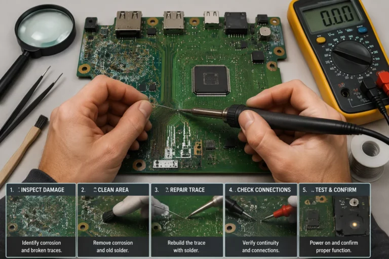
PCB electrical testing finds shorts, opens, and other connection defects. It does this by sending electrical signals to the bare board and measuring the response. These three defect types cover the faults that matter most: unwanted bridges between traces, broken connections, and wrong net paths. Electrical testing finds each one by measuring directly, not by guessing from looking. The sections below explain how these defects are found, the methods used, what testing cannot detect, and how it compares with AOI and X-ray. Readers will see where electrical testing fits and where other inspection tools do the work for a pcb build.
Key Takeaways
Electrical testing finds shorts, opens, and wrong connections. It does this by sending signals through the board and measuring the response.
Bed-of-nails fixtures check many points at the same time to save time, while flying probe testing moves probes from point to point for more flexibility.
Electrical testing can’t find hidden problems. These include copper thickness, internal voids, or cosmetic flaws.
Use electrical testing along with AOI and X-ray to catch all kinds of defects.
Put test points in place early, check the netlist, and test again after rework to keep boards reliable.
What PCB Electrical Testing Is
PCB electrical testing sends electrical signals to a bare or assembled board. It then measures the resistance or continuity response. The tester compares each measurement against the netlist, the data file that lists every intended connection. A board passes when every net matches the design and no unintended path exists. This check gives direct proof that the board matches the design connectivity.
Electrical Test Versus Visual Inspection
Visual inspection looks at surfaces. It finds missing parts, solder bridges, and obvious damage. Electrical testing confirms the actual connectivity that visual methods cannot verify. A board may look perfect yet still contain a short circuit, an open connection, or an unexpected component reading. Only electrical testing (such as flying-probe testing) can expose these defects.
The two methods see different things, as the table below shows.
Aspect | Visual Inspection | Electrical Testing |
|---|---|---|
Internal or hidden shorts | Cannot detect | Detects via continuity checks |
Micro-cracks within layers | Cannot detect | Detects opens or shorts from cracks |
Electrical performance issues | Cannot detect | Verifies functionality |
Surface-visible defects | Can detect | Not its primary purpose |
Impedance mismatches | Cannot detect | Detects incorrect values |
Internal via breaks | Cannot detect without advanced tools | Detects through functional verification |
Visual inspection is still valuable for surface work. Electrical testing answers a different question: does the board actually conduct as designed?
How Signals Reveal Connectivity
The tester sends a signal through one point and reads the response at another. A low resistance between two points that should be isolated signals a short. A high resistance along a path that should conduct signals an open. This approach verifies the continuity of all nets in a single pass.
An e-test therefore catches faults that leave no visible trace. The netlist defines the expected pattern, and the tester flags any deviation. Coverage depends on probe access to test points, so designers should place test pads with this step in mind. A pcb built without test access limits what the tester can confirm.
Defects Electrical Testing Detects

Opens, Shorts, and Incorrect Nets
A bare board test checks the board against the netlist and marks any mismatch. The tester looks for three main things: continuity along every path it should have, isolation between paths that should stay apart, and full agreement with the design data. This check catches the most common electrical faults in one pass.
Open circuits: a path that should conduct shows high resistance or no continuity at all.
Short circuits: two nets that should stay apart show a low-resistance bridge, and the fault can make the circuit work incorrectly.
Incorrect net connections: a trace reaches the wrong pad, so the board conducts but not the way it was designed.
Broken traces: a partial or full break in a conductor stops the signal from flowing.
Missing vias: a layer-to-layer connection never forms, so nets stay isolated.
Many of these defects can’t be seen by eye. A short under a component or a hairline crack inside a trace leaves no mark on the surface. Isolation testing confirms that no unwanted shorts exist between traces, and continuity testing confirms that every net conducts. Together, these two checks give pcb electrical testing its main power. A board that passes both matches its design connections, and a board that fails points the technician to a specific net.
Broken Traces and Missing Vias
Broken traces and missing vias are both open faults, yet each fails in its own way. A broken trace usually comes from a scratch, an etch fault, or a flex crack. The conductor narrows or splits, and resistance climbs until the signal weakens or stops. A missing via breaks the vertical link between layers. The outer traces look fine, and the board still passes a quick look. Only an e-test that probes both ends of the net finds the gap.
Electrical tests handle both cases the same way: they measure end-to-end continuity against the netlist. A failed reading flags the net, and the technician traces the fault to the break or the missing via. This step matters on multilayer pcb builds, where inner-layer faults hide completely from view. Solder bridges on assembled boards also fall into this group, and in-circuit testing catches them by checking isolation between adjacent pins.
The defect list above shows why electrical testing is the base for connectivity checks. Opens, shorts, incorrect values, and missing parts all produce a measurable electrical signature. A tester reads that signature directly, so the result reflects real behavior rather than appearance. That directness sets electrical testing apart from every visual method, and it explains why bare board tests check the board against the netlist for shorts or opens before any assembly begins.
Bed-of-Nails and Flying Probe Testing

Two kinds of hardware do electrical testing on production boards. Each one works best for a different volume and design stage.
Fixture-Based Bed-of-Nails
A bed-of-nails fixture holds a grid of spring-loaded probes. Each probe presses down on a test point on the pcb. The tester then touches all nodes at once and reads every net at the same time. This parallel access makes the method very fast. Bed-of-nails ICT finishes tests in 5–15 seconds per board, so thousands of boards can be tested daily without operator fatigue. A typical cycle runs 5–10 seconds per board. The fixture finds opens, shorts, wrong components, and missing parts in that single pass.
The trade-off is in the fixture itself. Cost and setup grow with board complexity.
Limitation Category | Detail |
|---|---|
Fixture cost | Development-grade fixtures start around $999; production-grade fixtures cost $5,000–$15,000+ |
Complex boards | Custom fixtures can exceed $30,000, which makes the method less workable for runs under 500 units |
Design-specific setup | A test point moved by even 0.05 inches can make the fixture useless |
Setup time | Fixtures take weeks to design and build |
Flying Probe Testing
Flying probe testing uses moving probes that travel to each test point in turn. No dedicated fixture is needed. The system is programmed in hours rather than weeks, which fits prototypes and low-volume builds. Flying probe testing finds shorts, opens, resistance and capacitance problems, polarity errors, micro-shorts, reversed components, and missing parts. It also catches passive component value errors, open solder joints, and track impedance deviations through a 4-wire Kelvin test.
The method is slower because probes move point by point. Test time grows with node count, since each point is contacted sequentially. On a 500-point board, the step-by-step path explains the gap against bed-of-nails.
KING FIELD offers fly-probe, AOI, X-ray, and 100% function testing as part of its manufacturing flow. The One-Stop Industrial PCBA – LED Driver and Inverter PCB Assembly – 5-7 Days Prototype – 100% AOI and X-Ray Tested shows how these methods combine on one build. The service runs fly-probe, AOI, X-ray, and 100% function testing to find shorts, opens, missing components, incorrect values, and other electrical faults before shipment.
What Electrical Testing Cannot Detect
Copper Thickness, Voids, and Reliability
Electrical signals only show that a net conducts. They do not tell you how well the copper carries current over time. Copper thickness, internal voids, and long-term reliability are beyond what an e-test can confirm. A void inside a via may still pass continuity, but the thin wall can crack under thermal cycling later. A board can pass every net check and still fail in the field.
Some faults hide even from a passing reading. Barrel cracks from improper desmear, poor adhesion of barrel walls, and eventual inner layer separation can stay undetected until pcb electrical testing or, worse, only during field use. Hidden internal layer issues and defects that never show as electrical failures also fall outside the test’s reach. The method is limited to electrical functional faults, so its detection range and precision have limits. A technician reading a pass result should treat it as proof of connection, not proof of build quality.
Cosmetic Issues and the AOI/X-ray Comparison
Cosmetic flaws — scratches, solder mask discoloration, marking errors — leave no electrical signature. AOI and X-ray cover that ground. AOI catches surface placement and soldering faults fast, while X-ray goes through the board to image hidden joints, voids, and cracks. Each tool answers a different question about the same board. Neither replaces the other, and neither replaces electrical testing.
Criterion | AOI | X-ray | Electrical Test |
|---|---|---|---|
Defect detection | Surface features | Internal structures | Opens, shorts, net errors |
Internal voids | No | Yes | No |
Functional verification | No | No | Yes |
Reliability prediction | No | Partial (voids, cracks) | No |
The three methods work well together. AOI handles rapid surface faults, X-ray images hidden joints, and the tester verifies connectivity that visual methods cannot confirm. A pcb build that runs all three closes more gaps than any single tool. Checking connectivity remains the one job only the tester does, and that is why a pcb line keeps it in the flow.
E-Test Coverage, Yield, and Quality Fit
Netlist Accuracy and Coverage Factors
Coverage credibility depends on three things. The test program must match the correct design, the chosen method must reach the mapped targets, and the report must name the population measured. An accurate netlist exported from CAD lets the manufacturer cross-check Gerber files, catch CAM errors at data review, and verify coverage against design intent. Without a supplied netlist, connectivity is pulled from the Gerber files themselves. That approach works, but any file error goes straight into the test program.
Coverage control | Required input | Failure mode |
|---|---|---|
Electrical intent | CAD netlist or agreed fabrication data | Program encodes wrong connectivity |
Revision match | Board, data, and program on same revision | False pass or false fail |
Contact availability | Mapped targets reachable by the method | Nets reported separately |
Approved exclusions | Named excluded nets with reason | Reported coverage exceeds executed range |
Build-Flow Placement and Yield Control
Electrical testing shows up at several points in the build flow. The bare board is tested once solder mask, legend, and surface finish are applied, before shipment. Higher volumes often use bed-of-nails fixtures, while flying-probe systems fit prototypes and low-volume runs. After SMT reflow and AOI, assembled boards go through electrical and functional testing. Boards that pass then move to conformal coating, panel separation, and final inspection. Boards coming back from repair or rework re-enter the same gate, so a fix never ships unverified.
This placement supports yield control. A failed board is screened out before it uses more labor and material downstream. Low yield signals process instability or a design-manufacturing mismatch, which prompts corrective action. Stable upstream processes paired with inspection keep yield high over time and lower the effective cost per board.
An e-test does not stand alone. It joins AOI and X-ray inside a broader quality system. KING FIELD shows that framework with ISO9001, IATF16949, ISO13485, ISO14001, UL, and RoHS certifications. Each tool covers a different defect class, and the e-test closes the connectivity gap that visual methods cannot confirm.
Electrical testing is still the only way to directly check that a board’s connections really work. That is why it is the main check for shorts, opens, and wrong net connections on every build. No visual tool can prove that a net truly carries a signal.
Readers should use it together with AOI and X-ray for defects it cannot see. Each tool does a different job, and no single method is best at everything. Picking the right tool for each job keeps the line running well.
A helpful tip: run the e-test at the right stage and coverage level for the build. Place test points early, confirm the netlist, and test again after rework. This keeps pcb electrical testing and the whole pcb flow reliable from prototype to high volume.
FAQ
How fast does each electrical test method run?
A bed-of-nails fixture reads all nets at once, so a board clears in seconds. Flying probe moves point by point, so test time stretches to minutes and grows with node count. Volume and design stage decide which method fits.
Can a board pass testing and still fail in the field?
Yes. A void inside a via may still pass continuity, yet the thin wall can crack under thermal cycling later. A pass result proves connection, not build quality. Pair the e-test with X-ray to catch hidden structural faults.
Why does an inaccurate netlist weaken test coverage?
The tester judges every reading against the netlist. A wrong or outdated file encodes wrong connectivity, so the program flags good boards or clears bad ones. Confirm the netlist revision before the test program is built.
Does a repaired pcb skip electrical testing?
No. Boards returning from repair or rework re-enter the same test gate. A fix never ships unverified. This rule keeps yield data honest and stops a reworked pcb from carrying a new fault downstream.
Which defects stay invisible to electrical testing?
Copper thickness, internal voids, long-term reliability, and cosmetic flaws leave no electrical signature. AOI and X-ray cover that ground. Each tool answers a different question, and the tester confirms connectivity alone.