 English
 Arabic
 Chinese (Simplified)
 Dutch
 French
 German
 Italian
 Portuguese
 Russian
 Spanish


A PCB edge connector is the set of traces and metal pads on the edge of a circuit board that plug into a matching socket. This connector links one board to another board or to a device, and it carries power and signals between them. Inside the socket, small spring contacts press against the pads to complete the electrical path. The pad layout along the edge defines how the connector PCB edge fits into its mating part. Designers choose this edge style when a board needs frequent plugging and unplugging.
Key Takeaways
A PCB edge connector has metal pads on the edge of the board. These pads plug into a socket to carry power and signals.
Spring contacts inside the socket press against the pads. This makes a reliable electrical connection.
Hard gold plating on the pads helps the connector last through many plug and unplug cycles.
Designers have to line up the pad layout and pitch with the socket so it fits right.
Always check the connections after setup to make sure every pad touches.
What Is a PCB Edge Connector?
Definition and Anatomy
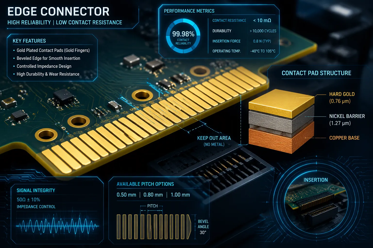
A PCB edge connector is the portion of a board where traces that lead to the board’s edge end in exposed metal contacts. These contacts are built to be plugged in to a socket on another board or device. The connector pcb edge carries power and signals between the two parts. Designers pick this style when a board must go in and out many times. The pcb edge connector turns the board itself into the plug, so no separate plug part is needed. The metal contacts along the edge form the plug face.
The anatomy starts at the edge of circuit boards. Traces run outward and end in flat pads called gold fingers. People also call them edge fingers or edge connector fingers. A thin nickel layer sits under the gold, and the gold layer takes the wear. The LinkedIn guide from Antti Rayming lists a typical gold thickness of 30 to 50 microinches. A bevel on the leading edge guides the board into the socket. Pads may sit on one side or on both sides. A single row suits simple links, and multiple rows pack more signals into the same length. Pitch is the center-to-center distance between neighboring pads. A smaller pitch fits more contacts in the same space. Many pcb edge connectors use a bevel angle of 20 to 60 degrees. Eurocircuits sets a keepout of 2.00mm between the inner end of the fingers and any plated hole or pad. Edge fingers can sit up to 1 inch deep from the outer edge. The edge fingers need a clean keepout. Edge connectors usually use hard gold for this reason.
Layer | Material | Job |
|---|---|---|
Base | Copper | Carries the signal |
Barrier | Nickel | Blocks diffusion and adds a hard base |
Surface | Hard gold, 30 to 50 microinches typical | Resists sliding wear |
Queen EMS notes that connector makers often ask for gold to ASTM B488 Type II, Grade C hardness.
How the Contact Mechanism Works
The board slides into a matching slot. Spring contacts inside the socket press against the edge fingers. Each spring stores energy and pushes back, so the pad and the contact stay joined. Wenda Electronics reports that contact geometry and spring force decide how well the parts engage. Too little force raises contact resistance. Too much force wears the gold. Suppliers of circuit board edge connector sockets tune each spring to a set force. TE describes a preloaded spring finger that nearly doubles the working area and adds 0.2N of force. Some designs add pre-wipe pads near the opening. These pads wipe the edge fingers clean and shorten the unused stub of the finger. Guide rails and keys keep the board square in the mating slot, so every spring loads evenly. A full seat matters, so the connector pcb edge must sit square in the socket. A partly inserted board can bend a spring or miss a pad. A gold-finger edge connector suits repeated insertion. A gold edge connector with gold-plated contacts along the edge lasts longer than a plain finish.
Main Types of Edge Connectors
Single-Sided vs. Dual-Sided
Single-sided edge connectors put exposed metal contacts on just one side of the board. This setup keeps the design simple and works well for low-cost boards with a small number of signals. Dual-sided edge connectors place pads on both the top and bottom faces. The second row doubles the contact count without making the board longer. Designers pick dual-sided layouts when a pcb edge connector has to carry many signals in a small space. Both styles depend on the same spring-contact idea inside the matching socket.
The choice comes down to the signal budget and the board area you have. A single-sided board is a good fit for a simple link between two assemblies. A dual-sided board works for denser designs, like backplanes and expansion cards. Neither style wins in every case. Each one fits its own set of needs.
Connector PCB Edge Options Compared
Contact layout and socket mounting style shape the final design. Single-row connectors use one line of contacts and fit low-to-moderate signal counts, like a small Arduino shield, according to PCBMaster. Multi-row connectors use two or more lines and serve complex circuits, like a server backplane that handles dozens of signals. Unikeyic notes that dual-row headers show up often in development boards and industrial control boards.
Type | Contact layout | Best use |
|---|---|---|
Single-row | One line of contacts | Low-to-moderate signal counts |
Multi-row | Two or more lines | Complex circuits, parallel signals |
Through-hole socket | Pins soldered through the board | Prototypes, repairs, low-volume fixtures |
Surface-mount socket | Pads reflowed on the surface | Tight height limits, automated assembly |
Mounting style changes more than PCB area, Soulin warns. An SMT header can shrink the footprint but still block a cable path. A through-hole option may give better mechanical support but still needs room for soldering and rework. Alibaba’s buying guide sums up the trade-off well.
Through-hole for repair and hand-soldering; SMT for production; hybrid only if geometry mismatch exists.
A gold-finger edge connector with a through-hole socket works well for field service. An SMT socket works well for scalable production. The right edge connector matches the signal count, the space, and the build volume.
Designing a Printed Circuit Board Edge Connector
Pitch, Materials, and Footprint
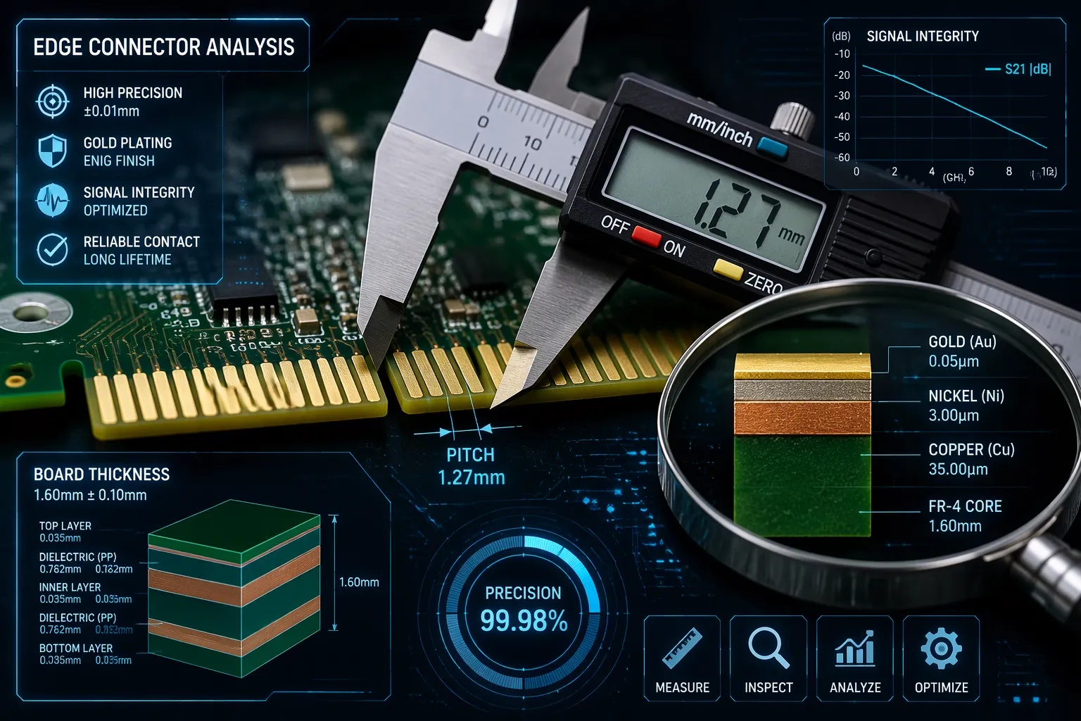
Pitch is the center-to-center distance between pads that sit next to each other on the connector pcb edge. A finer pitch fits more contacts on a shorter edge. A coarser pitch gives each pad more room so it can handle wear. Designers match the pitch to the socket they plan to use. The footprint must copy the socket exactly, so pad width, gap, and row spacing all follow the mating part’s drawing.
The plating you choose decides how long the edge fingers last. Hard gold over a nickel underlayer gives the best wear life. A 30 microinch layer suits moderate use, while thicker hard gold fits higher cycle counts. Going above 50 microinches risks cracking, and dropping below 30 microinches risks exposing the nickel. Soft gold serves wire bonding, not repeated plugging. ENIG is thin and soft and is unsuited for boards subject to abrasive insertion and removal, and tin plating is the cheapest option but oxidizes easily.
Plating | Thickness | Insertion Cycles | Best Fit |
|---|---|---|---|
Hard gold | 30 to 50 microinches over nickel | Not specified | High-wear, high-reliability boards |
ENIG | 2 to 5 microinches gold | Not specified | Moderate wear, cost-sensitive builds |
Soft gold | Not specified | Not specified | Wire bonding, not frequent insertion |
Tin | Not specified | Not specified | Lowest cost, low-reliability use |
Board thickness affects mating force and bevel geometry. Eurocircuits specifies a minimum PCB thickness of 1.00mm and a maximum of 3.20mm for edge connectors. A board that is too thin may miss the socket pins, and one that is too thick can stress the connector. Eurocircuits lists a standard bevel angle of 30 degrees, with special angles of 20, 30, 45, and 60 degrees, and a minimum remaining material thickness of 0.25mm after beveling. The chamfer must happen after hard gold plating, so the cut edge stays clean.
Signal and power layout bring their own rules. Keep the stub between the last pad and the inner trace short, because a long stub adds reflection and weakens high-speed signals. Align every pad to the socket datum, since a small shift loads some springs harder than others. Specify enough gold thickness for the cycle count, or the nickel will show through and raise contact resistance. Route power pads wider than signal pads to carry current without heating.
KING FIELD Design Support
KING FIELD supports edge connector designs through its PCB fabrication and assembly services. The company builds multilayer and HDI boards, which helps when a dense pcb edge connector needs many layers and fine features. Strict quality control and multiple testing services back each build. Designers can send a gold-finger edge connector layout and let KING FIELD handle fabrication, plating, and assembly in one flow.
Installing and Testing Edge Connectors
Mating and Installation Steps
A clean installation starts with alignment. The installer lines up the bevelled leading edge of the board with the opening of the socket. The bevel guides the board into the slot and prevents the corner from catching a spring contact. A square approach matters, because a tilted board can bend a spring or miss a pad.
The next steps follow a steady rhythm:
Align the board edge with the socket opening and check that the key or guide rail matches the board.
Slide the board in evenly with light, straight pressure. Never force it or rock it side to side.
Push until the board seats fully. A partly seated pcb edge connector can leave some contacts unloaded.
Check the seating depth against the socket marking or a visual line on the board.
A full seat keeps every spring loaded at the same force. Installers should confirm the board sits square before they apply power.
Continuity and Reliability Testing
Testing proves that each pad meets its spring. A continuity check sends a small current through every contact pair and confirms a closed path. A contact resistance test goes further and measures the joint quality. High resistance points to weak spring force, dirt on the edge fingers, or worn gold.
High-mating-cycle products need cycling checks. The tester plugs and unplugs the board repeatedly, then repeats the continuity and resistance checks. Edge connectors suit applications that need more plug and unplug cycles than standard boards, so this step protects long-term reliability. A simple pass/fail log for each contact keeps the results easy to review.
Test | What it checks | When to run it |
|---|---|---|
Continuity | Closed path at every contact | After each mating |
Contact resistance | Joint quality and spring force | First build and after cycling |
Cycling check | Wear over many insertions | High-cycle designs |
PCB Edge Connector Applications
Common Real-World Uses
Edge connectors appear anywhere a board has to slide in and out of a system. One common job is linking one PCB to another, like a daughter card that plugs into a motherboard. Driver boards also connect to LED array boards through an edge connector to carry power to the lights. Expansion cards in computers work the same way, with gold edge fingers sliding into a slot on the main board. Industrial, medical, and automotive circuit boards use this design too, because field service often means swapping a module instead of replacing a whole unit.
Each of these uses depends on the same strength. The board itself becomes the plug, so the assembly stays compact and the mating action stays simple. A technician can pull a module and push in a replacement without touching a cable.
Matching the Connector to the Use Case
The right choice starts with the signal. SLLPCB advises designers to treat the connector and the PCB transmission line as one high-speed interconnect. That means checking impedance, insertion loss, and crosstalk when data rates climb. Power needs follow a different path. SLLPCB notes that power and high-speed signal applications may need very different connector technologies even when their physical sizes look alike. Designers should plan around continuous current, not just a peak rating.
Pitch and plating close the loop. SLLPCB lists common pitches from 2.54 mm down to 0.40 mm and smaller, and a finer pitch saves board area at the cost of tighter fabrication control. Soulin Connector adds that tin suits standard-duty work, while gold fits frequent mating or high-reliability signals. A serviceable industrial device may need far more mating cycles than a board assembled once at the factory. The table below sums up the fit.
Need | Selection focus |
|---|---|
High-speed data | Impedance, loss, crosstalk |
Power delivery | Continuous current, voltage rating |
Frequent mating | Gold finish, cycle rating |
Tight space | Fine pitch, SMT socket |
A pcb edge connector is a row of exposed pads on the board edge that slides into a matching socket. Spring contacts inside that socket press against the pads and complete the circuit. This simple pairing of edge fingers and a socket carries power and signals between boards.
Practical choices still decide the result. Designers pick the right connector type, follow pitch and footprint rules, and test every contact after installation. Beginners should start with a simple gold-finger edge connector, check contact on each pad, and scale up once the design proves reliable. KING FIELD offers delivery and assembly help for that next step.
FAQ
What does a PCB edge connector do?
It turns the board edge into a plug. Traces end in exposed pads, and those pads slide into a socket on another board. The joint carries power and signals between the two assemblies. Designers choose this style when a module needs frequent swapping.
How many times can edge fingers survive plugging?
The answer depends on the plating. Hard gold at 30 to 50 microinches over nickel is the typical wear-resistant finish. A thinner 30 microinch layer suits moderate use. Soft gold fits wire bonding rather than repeated mating.
Why does gold plating matter on the contacts?
Gold resists sliding wear and keeps resistance low. A nickel layer sits underneath and blocks diffusion. Too little gold exposes the nickel, and contact resistance climbs. Too much gold risks cracking. Designers match the thickness to the expected cycle count.
How does a board stay aligned in the slot?
A bevel on the leading edge guides the board into the opening. Keys and guide rails keep it square, so every spring loads evenly. The installer pushes straight until the board seats fully. A tilted or partly seated board can bend a spring.
Do pcb edge connectors need testing after installation?
Yes. A continuity check confirms a closed path at every pad. A resistance test reveals weak spring force or worn gold. High-cycle designs also need repeated plug and unplug checks. A simple pass/fail log for each contact keeps results easy to review.