 English
 Arabic
 Chinese (Simplified)
 Dutch
 French
 German
 Italian
 Portuguese
 Russian
 Spanish

PCB Routing Best Practices: Optimize Signal Flow and Design Rules
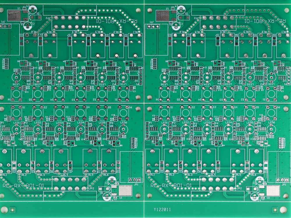
Designing a PCB involves a delicate balance of technical and practical considerations, especially when high-speed signals are involved. This guide explores the intricate world of high-speed PCB routing and offers insights into best practices, advanced techniques, and practical applications.
Introduction
What is PCB Routing?
PCB routing is the process of designing the electrical paths, or traces, on a printed circuit board (PCB) to connect various components per the schematic. In high-speed and high-frequency applications, routing becomes critical, as it directly influences the signal integrity and overall performance.
During the routing process, design choices like trace width, spacing, via placement, and layer transitions play a crucial role in maintaining signal integrity. Proper planning and execution can reduce signal reflections, crosstalk, and electromagnetic interference (EMI).
Key Aspects:
- Signal Paths: The physical copper traces that connect different components.
- Differential Pairs: Routing two complementary traces to maintain balanced signals.
- Via Design: Using vias for layer transitions but avoiding stubs that cause reflections.
PCB Routing vs. PCB Layout
PCB layout refers to the broader process of organizing the board’s components, traces, power planes, and more. It involves strategic component placement and layer stack-up design to optimize space and performance.
On the other hand, PCB routing is specifically focused on the connections between components. The goal is to create pathways that preserve the electrical properties of the signals being transmitted.
| Aspect | PCB Layout | PCB Routing |
|---|---|---|
| Scope | Overall board design | Signal path design |
| Key Elements | Component placement, stack-up | Trace width, spacing, vias |
| Focus | Mechanical fit, manufacturability | Signal integrity, performance |
| Workflow | Planning and arranging | Drawing and configuring paths |
FastlinkPCB’s Role in PCB Routing Optimization
FastlinkPCB’s Expertise in High-Speed PCB Routing
FastlinkPCB offers specialized services in high-speed PCB routing, ensuring that the complex requirements of modern electronics are met with precision. They utilize cutting-edge technology and expert knowledge to optimize PCB routing for high-performance circuits.
Core Functions:
- Signal Integrity Analysis: Utilizing advanced simulation tools to predict and enhance the electrical performance of PCB designs.
- Customized Solutions: Tailoring designs to meet specific industry standards and client needs.
- Collaboration with Manufacturers: Ensuring that design choices align with manufacturing capabilities to maintain high yield and reliability.
Nine Best Practices for PCB Routing
Implementing these best practices ensures optimal performance and reliability in high-speed PCB design:
1. Start Before Traces are Laid Out
Begin with strategic planning:
- Component Placement: Align components to reduce trace length and enhance connectivity.
- Prioritize Critical Signals: Define paths for sensitive signals like clocks and high-speed data lines early in the design process.
2. Multilayer Stack-up
Employ a well-thought-out multilayer PCB stack-up:
- Scenario 1: Multilayer PCB: Provides multiple routing layers and consistent ground references.
- Scenario 2: 2-Layer PCB: Use sparingly; maintain continuous ground whenever possible.
Table: Multilayer Stack-up Benefits
| Layers | Benefits |
|---|---|
| 4-layer PCB | Balanced cost/performance |
| 6-layer PCB | Better impedance control |
| Multilayer | Advanced EMI shielding |
3. Efficient Ground Planes
Design solid ground planes for stability:
- Avoid Split Planes: Ensure continuous paths for return currents.
- Ground Stitching Vias: Connect separate ground areas to minimize EMI.
4. Via Placement
Optimize via usage:
- Grid Pattern: Prevents plane voids and hot spots.
- Consider Stub Length: Minimize unnecessary via barrel lengths to reduce reflections.
5. Spacing and Crosstalk Reduction
Increase spacing between traces outside dense areas to mitigate crosstalk. Utilize appropriate routing rules to ensure signals are isolated and can propagate without interference.
6. Stub Length Minimization
Prevent signal integrity issues by:
- Back-Drilling: Remove unused portions of through-vias.
- Direct Routing: Reduce the need for test-point branches.
7. Differential Pair Symmetry
Maintain consistency in differential pair routing:
- Balanced Traces: Ensure equal path lengths and spacing for consistent impedance.
8. Propagation Delay Matching
Ensure timing alignment across traces:
- Physical vs. Electrical Length: Consider the dielectric constant and layer properties.
- Scenario Planning: Develop plans for parallel data or address bus scenarios.
9. Avoid Split Planes
Prevent routing over split planes to maintain a low-impedance return path:
- Stitching Capacitors: Allow transitions between reference planes without interruptions.
These best practices form the foundation of effective PCB routing. When you’re ready, let me know to continue with the next section: A Complete Guide to PCB Routing.
A Complete Guide to PCB Routing
PCB Design Guidelines
Effective PCB routing adheres to a comprehensive set of design guidelines, covering various aspects like trace width, spacing, via placement, and multilayer stack-up considerations.
1. Trace Width and Spacing
Trace geometry impacts signal integrity, current carrying capacity, and impedance. Accurate calculation ensures that traces perform as expected.
- Controlled Impedance: Essential for maintaining signal integrity in high-speed PCB designs.
- Adequate Spacing: Prevents crosstalk and EMI issues, especially in densely populated areas.
Table: Trace Width and Impedance Control
| Parameter | Importance |
|---|---|
| Trace Width | Affects impedance |
| Trace Spacing | Minimizes crosstalk |
| Dielectric Constant | Influences signal speed |
2. Via Types and Placement
Different via types and placements influence the electrical properties and manufacturability of a PCB.
- Through-Hole Vias: Common but may create stubs; careful planning required.
- Microvias: Ideal for HDI designs, providing efficient layer transitions.
High-Speed Routing and Signal Integrity
Routing high-speed signals demands careful consideration of potential reflections, losses, and interferences.
Signal Integrity Considerations
- Transmission Lines: Ensure controlled impedance and reduce reflections.
- Eye Diagram Integrity: Measure signal quality by evaluating waveform at the receiver.
Crosstalk and EMI Reduction
- Trace Separation: Adequate spacing reduces unwanted coupling.
- Ground Plane Design: Continuous planes offer effective EMI shielding.
Thermal Management
Thermal management is vital for the reliability and performance of high-speed PCBs.
- Thermal Vias and Pads: Facilitate heat dissipation.
- Component Placement: Strategically place heat-generating components to minimize hotspots.
Observe DFM Policies
Design for Manufacturability (DFM) ensures that a design can be efficiently and reliably produced. Collaborating with manufacturers early in the design process helps identify potential issues and adapt designs accordingly.
- Tolerance and Clearance Compliance: Align design specifications with fabrication capabilities.
- Solder Mask Openings: Ensure proper mask design for effective soldering.
Advanced Techniques in PCB Routing
Differential Pair Routing
Implement structured routing strategies for differential pairs:
- Matched Lengths: Maintain equal electrical lengths to reduce skew.
- Consistent Spacing: Required for balanced impedance.
Controlled Impedance Routing
Maintaining controlled impedance is key for signal integrity in multilayer PCBs. Calculating accurate trace width, spacing, and dielectric properties ensures a consistent electrical environment.
Via Stitching for EMI Shielding
Via stitching connects ground planes across layers, enhancing EMI shielding and maintaining a continuous reference plane.
Length Matching for Synchronized Signals
Synchronizing signal propagation by closely matching trace lengths or electrical delays ensures timing alignment across channels.
Conclusion
High-speed PCB routing is a complex yet essential aspect of modern electronic design, impacting everything from signal integrity to manufacturability. By leveraging best practices and advanced techniques, engineers ensure efficient pathways that preserve signal quality, reduce electromagnetic interference (EMI), and manage thermal challenges.
A well-designed PCB considers all elements: from trace width and spacing to thermal management and DFM policies. Collaboration with manufacturers and using tools like FastlinkPCB’s advanced routing technology ensures that boards are not only functional but also optimized for performance and reliability.
FAQs
What does routing on a PCB mean?
Routing on a PCB involves creating the electrical paths that connect components on the board, ensuring signals are transmitted efficiently and accurately according to the schematic.
What are common PCB routing rules for manufacturing?
Common rules include maintaining adequate trace width and spacing, properly placing vias, ensuring controlled impedance, and adhering to the manufacturer’s design capabilities for fabrication.
What benefits do multilayer PCBs offer for routing?
Multilayer PCBs provide multiple routing layers, helping to manage high-density designs, reduce EMI, and maintain consistent ground and power planes for improved signal integrity.
How does FastlinkPCB optimize routing?
FastlinkPCB utilizes advanced design tools and methodologies to optimize routing, focusing on signal integrity, manufacturability, and overall performance, ensuring designs meet both industry standards and specific client needs.