PCB Assembly Process Unveiled with Key Insights
The PCB assembly process transforms a bare printed circuit board into a fully functional electronic device. This intricate process involves mounting components, soldering, and rigorous testing to ensure optimal performance. Understanding this process is essential for achieving high-quality results in electronics manufacturing.
Effective quality control can significantly enhance efficiency and reliability. For instance:
- The lot reject rate (LRR) can improve from 5500 parts per million (PPM) to 900 PPM.
- Fault rates may decrease by 0.76%, leading to fewer errors during production.
- Industry benchmarks show yield rates improving up to 95% with robust quality measures.
By grasping the nuances of PCB assembly, you can ensure your devices meet performance standards while minimizing defects.
Key Takeaways
- Learning how PCBs are made is important for good electronics. Focus on each step to avoid mistakes.
- Use Design for Assembly (DFA) rules to make building easier. Fewer parts and common pieces mean fewer problems.
- Use Automated Optical Inspection (AOI) to find mistakes early. This tool improves quality and meets industry rules.
- Check and test carefully, like using x-rays and function tests. This makes sure PCBs work well and last long.
- Keep clear records during the process. Good records help with recalls and build customer trust.
Preparing for the PCB Assembly Process
Design for Assembly (DFA) and File Preparation
Design for Assembly (DFA) plays a pivotal role in streamlining the pcb assembly process. By focusing on simplifying the assembly of a printed circuit board, DFA minimizes errors and enhances efficiency. For instance, using fewer parts reduces the chances of defects, while standardized components improve consistency. Features like self-alignment prevent misassembly, ensuring a smoother process. The table below highlights key benefits of DFA:
| Benefit of DFA | Description |
|---|---|
| Fewer parts | Reduces opportunities for defects |
| Simplified assembly | Decreases operator errors |
| Standardized components | Enhances consistency |
| Self-aligning features | Prevents misassembly |
| Reduced fastener count | Minimizes loosening and failure points |
File preparation is equally critical. You must ensure that design files, including Gerber files and assembly drawings, are accurate and complete. These files guide manufacturers in placing components correctly and avoiding costly mistakes.
Bill of Materials (BOM) and Component Sourcing
A well-prepared Bill of Materials (BOM) is the backbone of any successful pcb assembly. It lists all components required for the printed circuit board, including part numbers, quantities, and specifications. A clean and detailed BOM reduces ambiguity, ensuring that manufacturers source the right components. At Sierra Circuits, engineers meticulously verify BOMs to minimize errors and optimize costs.
Component sourcing demands careful attention. You should prioritize quality and reliability when selecting suppliers. Partnering with trusted vendors ensures that components meet industry standards and are readily available, preventing delays in the assembly process.
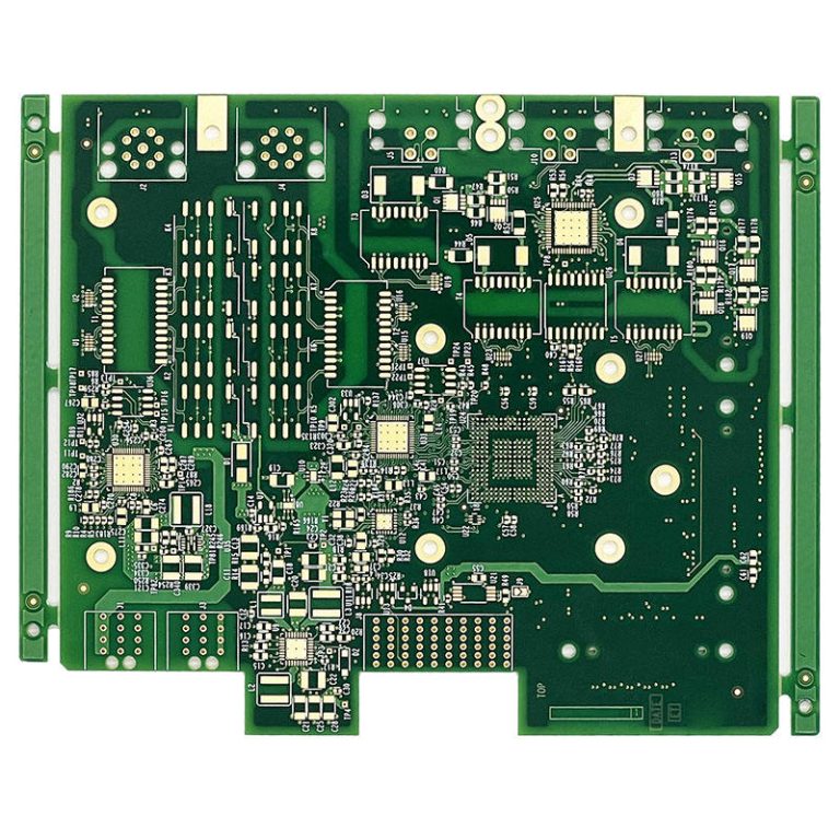
Initial PCB Inspection
Before starting the assembly, inspecting the bare pcb is essential. This step identifies potential issues such as surface defects, misaligned holes, or damaged traces. Addressing these problems early prevents complications during the assembly process. Automated tools like optical scanners can enhance the accuracy and speed of inspections, ensuring your printed circuit board is ready for the next stage.
Tip: Always align your preparation steps with product requirements to achieve better outcomes. Efficient planning and quality assurance can significantly improve the success rate of your pcb assembly process.
Component Placement in the PCB Assembly Process
Surface Mount Technology (SMT) Assembly
Surface Mount Technology (SMT) is a cornerstone of modern printed circuit board assembly. It involves mounting electronic components directly onto the surface of the pcb, eliminating the need for drilled holes. This method is highly efficient and supports miniaturization, making it ideal for compact devices like smartphones and wearables.
SMT assembly begins with applying solder paste to the pcb using a stencil. This paste acts as an adhesive and conductor for the components. Once the paste is applied, components are placed on the board using automated pick-and-place machines. These machines ensure precise placement, reducing errors and improving consistency.
Defect rates in SMT assembly are impressively low, as shown in industry data:
| Type of Defect | Defect Rate (PPM) |
|---|---|
| Solder defects | < 50 |
| Placement defects | 200-300 |
| Bad runs | Up to 2000 |
Despite its efficiency, SMT assembly requires careful monitoring to prevent issues like solder shorts and component misalignment. Automated Optical Inspection (AOI) systems play a vital role in detecting these defects early, ensuring high-quality results.
Through-Hole Technology (THT) Assembly
Through-Hole Technology (THT) assembly is a traditional method where components are inserted into pre-drilled holes on the pcb and soldered to pads on the opposite side. While SMT dominates modern manufacturing, THT remains essential for applications requiring strong mechanical bonds, such as industrial equipment and aerospace systems.
The THT process begins with manual or automated insertion of components into the pcb. These components are then soldered using wave soldering, a technique that ensures uniform solder coverage across multiple pins. THT assembly is particularly effective for large or heavy components that require additional stability.
Although THT offers durability, it is less efficient than SMT due to the manual labor involved. Traditional visual inspection methods, which rely on human operators, can increase costs and introduce subjectivity. Automated systems are gradually replacing manual inspections to enhance accuracy and reduce long-term labor expenses.
Note: THT assembly is ideal for high-power applications where reliability outweighs the need for compact designs.
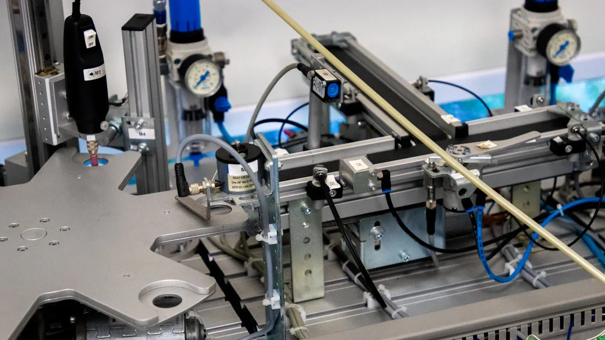
Pick-and-Place Machines and Techniques
Pick-and-place machines are the backbone of the pcb assembly process. These machines use robotic arms to pick components from feeders and place them accurately on the pcb. Advanced models can handle up to 15,000 components per hour, significantly speeding up production.
Modern pick-and-place machines offer unparalleled precision compared to manual methods. Manual placement often leads to longer inference times, higher labor costs, and increased risk of pcb damage due to physical handling. Automated systems eliminate these issues, ensuring consistent results and reducing defect rates.
Key features of pick-and-place machines include:
- High-speed operation: Rapid placement of components to meet tight deadlines.
- Vision systems: Cameras and sensors for precise alignment and error detection.
- Flexibility: Ability to handle various component sizes and shapes.
These machines are integral to both SMT and THT assembly, streamlining the process and ensuring high-quality outcomes. By leveraging automation, you can achieve faster turnaround times and lower defect rates, making your printed circuit board assembly more efficient and reliable.
Soldering Techniques in the PCB Assembly Process
Reflow Soldering for SMT Components
Reflow soldering is the most common method for attaching surface-mounted components to a pcb. This technique uses a controlled heating process to melt solder paste, creating strong and reliable connections. The process begins with applying solder paste to the pcb, followed by placing components onto the board. The assembly then passes through a reflow oven, where the temperature follows a specific profile to ensure optimal results.
A typical reflow soldering temperature profile includes four key zones:
| Zone | Description | Impact on Reliability |
|---|---|---|
| Preheating Zone | Gradually raises temperature to prevent thermal shock. | Prevents damage to sensitive components and avoids solder paste drying. |
| Soaking Zone | Holds temperature constant for uniform heating and flux activation. | Ensures consistent solder joint quality by minimizing temperature variations. |
| Reflow Zone | Reaches peak temperature to melt solder paste and form bonds. | Critical for optimal solder joint formation; prevents defects like cold solder joints. |
| Cooling Zone | Rapidly lowers temperature to solidify solder joints. | Controlled cooling prevents intermetallic compound formation that weakens joints. |
You can choose from different reflow profiles based on your project needs:
- Ramp-Soak-Spike (RSS) Profile: Controls temperature changes to prevent defects like solder bridging.
- Ramp-to-Spike (RTS) Profile: Features a continuous temperature increase, ideal for lead-free soldering.
- Custom Profiles: Tailored to specific pcb and solder paste requirements for better quality.
Reflow soldering ensures precision and efficiency, making it indispensable for modern printed circuit board assembly.
Wave Soldering for THT Components
Wave soldering is the go-to method for through-hole components. This process involves passing the pcb over a wave of molten solder, which coats and secures the component leads. It is particularly effective for high-volume production, as it provides uniform solder coverage across multiple pins in a single pass.
Before wave soldering, you must apply flux to the pcb to clean and prepare the surfaces for solder adhesion. The board then moves through a preheating stage to prevent thermal shock. Finally, it passes over the solder wave, where the molten solder bonds the components to the board.
Wave soldering is ideal for applications requiring strong mechanical connections, such as industrial equipment or aerospace systems. However, you should monitor the process closely to avoid defects like solder bridges or insufficient solder coverage.
Hand Soldering for Specialized Applications
Hand soldering remains essential for tasks requiring precision and flexibility. This technique is often used for prototypes, repairs, or low-volume production runs. You can also rely on hand soldering for components that automated machines cannot handle, such as odd-shaped parts or connectors.
To achieve high-quality results, you must use the right tools and techniques. A temperature-controlled soldering iron ensures consistent heat application, while high-quality solder paste improves joint reliability. Proper training is crucial, as manual soldering requires skill to avoid issues like cold solder joints or overheating.
Hand soldering offers unmatched adaptability, making it a valuable tool for specialized pcb assembly needs.
Inspection and Testing in the PCB Assembly Process
Inspection and testing are critical stages in the pcb assembly process. These steps ensure that the assembled boards meet quality standards and function as intended. By employing advanced inspection techniques, you can identify defects early, reduce errors, and maintain high production efficiency.
Automated Optical Inspection (AOI)
Automated Optical Inspection (AOI) systems are indispensable in modern pcb assembly. These systems use high-resolution cameras and advanced algorithms to detect defects such as soldering issues, missing components, and misalignments. AOI is particularly valuable for inspecting complex boards where manual inspection becomes impractical.
The increasing complexity of electronic devices has driven the demand for AOI systems. These systems enhance production efficiency by identifying defects early, allowing you to address issues before they escalate. Industries like consumer electronics, automotive, and aerospace rely heavily on AOI to meet stringent quality standards. Advanced AOI systems, powered by AI, achieve an impressive error detection accuracy rate of over 97%, as shown below:
| Accuracy Rate | Description |
|---|---|
| 97%+ | Achieved by advanced AI models in AOI systems. |
By integrating AOI into your assembly line, you can ensure consistent quality and reduce the risk of defective products reaching the market.
X-Ray Inspection for Complex Boards
X-ray inspection is a powerful tool for examining complex pcbs, especially those with hidden solder joints or densely packed components. This technique uses high-resolution imaging to detect internal defects that are invisible to traditional inspection methods. It is particularly effective for identifying issues like voids in solder joints, misaligned components, and internal cracks.
AI-driven x-ray systems have revolutionized fault detection by simplifying the identification of hard-to-spot flaws. These systems filter out noise, assess critical areas, and highlight potential defects, allowing you to focus on challenging issues while automating routine detections. High-end x-ray systems provide micro-focus images with resolutions as fine as 5 microns, ensuring unparalleled precision.
Key benefits of x-ray inspection include:
- Enhanced detection of soldering defects in hidden joints.
- Compliance with international standards like IPC-A-610 and IPC-6012.
- Inspection speeds exceeding 50 cm²/sec for high-volume production.
By leveraging x-ray inspection, you can achieve higher reliability and quality in your pcb assembly process, particularly for applications in aerospace and medical devices.
Functional Testing and Debugging
Functional testing is the final step in ensuring that your assembled pcb performs as intended. This process involves simulating real-world operating conditions to verify the board’s functionality. By conducting functional tests, you can identify and resolve issues such as signal integrity problems, power distribution errors, and software malfunctions.
Debugging complements functional testing by pinpointing the root causes of detected issues. Skilled engineers use specialized tools and techniques to analyze the board’s performance and implement corrective measures. This step is crucial for optimizing the board’s reliability and ensuring it meets the required specifications.
Functional testing and debugging are essential for delivering high-quality products. By investing in these processes, you can minimize the risk of field failures and enhance customer satisfaction.
Final Steps in the PCB Assembly Process
Cleaning and Final Touches
Cleaning is a critical step in ensuring the long-term reliability of your assembled pcb. Residual contaminants, such as flux and soldering byproducts, can compromise the performance of mission-critical electronics. Adhering to strict cleaning standards minimizes these risks and enhances the durability of your boards.
Recent studies highlight the importance of cleanliness in pcb assembly:
- Contamination can lead to reliability issues, especially in high-stakes applications.
- Strict cleaning standards correlate with improved long-term performance.
- Localized ionic and Surface Insulation Resistance (SIR) testing methods show a 76% effectiveness rate in assessing cleanliness.
You can use advanced cleaning techniques, such as ultrasonic cleaning or aqueous cleaning systems, to remove residues effectively. After cleaning, applying final touches like conformal coatings protects the pcb from environmental factors, including moisture and dust. These steps ensure your boards are ready for deployment in demanding conditions.
Tip: Always verify the cleanliness of your boards using industry-standard testing methods to avoid unexpected failures.
Packaging and Documentation
Proper packaging safeguards your assembled pcbs during transit and storage. Use anti-static bags and shock-resistant materials to prevent physical damage and electrostatic discharge. For bulk shipments, consider using custom trays or foam inserts to maintain the integrity of your boards.
Documentation is equally important. Provide detailed assembly notes, including soldering profiles, inspection results, and testing data. These records help manufacturers and end-users understand the assembly process and ensure compliance with industry standards. Clear documentation also facilitates troubleshooting and repairs, saving time and resources.
By prioritizing packaging and documentation, you can maintain the quality of your boards and streamline communication with stakeholders.
Ensuring Traceability and Compliance
Traceability is essential for minimizing the impact of product recalls and maintaining brand reputation. Implementing standards like IPC-1782 allows you to track every stage of the pcb assembly process, from component sourcing to final inspection. This level of control reduces the scope of recalls and ensures compliance with regulatory requirements.
For example, basic lot-control traceability can narrow down affected units in a recall from thousands to about 15,000 cars. Advanced traceability systems can reduce this number even further, as demonstrated by a case where only 990 cars were impacted due to precise defect identification.
Compliance with industry standards, such as IPC-A-610 and ISO certifications, ensures your boards meet quality benchmarks. By integrating traceability and compliance measures, you can enhance reliability, reduce costs, and protect your brand image.
Note: Investing in traceability systems not only mitigates risks but also builds trust with your customers and partners.
The PCB assembly process involves several critical stages, from preparation and component placement to soldering, inspection, and final touches. Each step plays a vital role in ensuring the functionality and reliability of your electronic devices. By implementing robust quality control measures, you can adhere to industry standards and prevent issues like counterfeit components or manufacturing defects. Continuous audits, statistical tools, and systematic documentation further enhance product quality and compliance.
A thorough understanding of this process empowers you to optimize efficiency and deliver superior results. Whether you’re designing for aerospace, medical devices, or consumer electronics, mastering the intricacies of PCB assembly ensures your products meet the highest benchmarks.
FAQ
What is the difference between SMT and THT assembly?
Surface Mount Technology (SMT) places components directly onto the PCB surface, enabling compact designs. Through-Hole Technology (THT) inserts components into drilled holes, offering stronger mechanical bonds. SMT suits miniaturized devices, while THT is ideal for high-power or durable applications like aerospace systems.
Why is Design for Assembly (DFA) important in PCB assembly?
DFA simplifies the assembly process by optimizing the design for manufacturing. It reduces errors, minimizes costs, and enhances efficiency. Features like standardized components and self-alignment improve consistency, ensuring your PCB assembly process runs smoothly and delivers high-quality results.
How does Automated Optical Inspection (AOI) improve quality control?
AOI uses cameras and algorithms to detect defects like soldering issues or missing components. It ensures early identification of problems, reducing production errors. With over 97% accuracy, AOI enhances reliability and helps you meet stringent industry standards.
What role does traceability play in PCB assembly?
Traceability tracks every stage of the assembly process, from component sourcing to final testing. It minimizes recall impacts, ensures compliance with standards like IPC-1782, and builds trust with customers. Advanced systems narrow defect identification, saving costs and protecting your brand reputation.
Can hand soldering replace automated soldering techniques?
Hand soldering complements automated methods but cannot replace them for high-volume production. It excels in specialized tasks like prototypes, repairs, or odd-shaped components. Skilled operators and proper tools ensure precision, making it a valuable technique for unique assembly needs.