 English
 Arabic
 Chinese (Simplified)
 Dutch
Dutch French
 German
 Italian
 Portuguese
 Russian
 Spanish
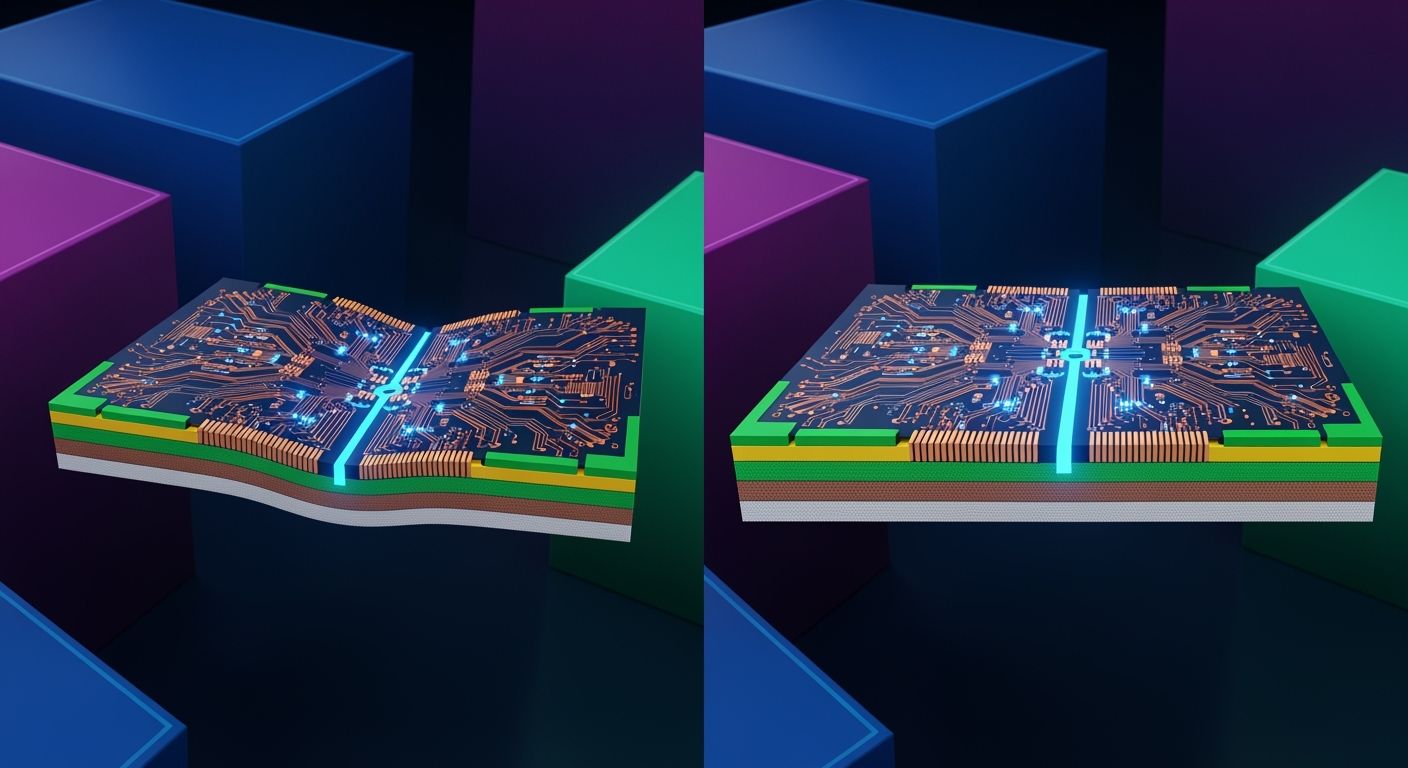
Uneven heating across unbalanced pcb layers creates different amounts of stress during lamination and high-temperature reflow near 260°C. Copper expands at 17 ppm/°C, while FR-4 substrate expands at 14-16 ppm/°C. You experience pcb warping when these unbalanced layers expand unevenly.
Proper pcb copper balance controls board planarity. Layout symmetry, layer placement, and copper density govern overall board flatness. This thermal alignment protects long-term electrical performance during automated assembly.
You can master copper balancing to prevent severe manufacturing defects. Effective copper balancing techniques like copper thieving equalize stress. You must maintain balance across every printed circuit board layer. Follow actionable IPC compliance thresholds to eliminate board bow and twist.
Key Takeaways
- Uneven heating makes copper and base materials grow larger at different rates.
- Uneven copper layers make the circuit board bend and twist.
- Evenly matching the board layers keeps mechanical stress low across the whole printed circuit board.
- Adding copper thieving keeps metal thickness even across open signal areas.
- IPC standards state that surface-mount boards must keep their physical warping under 0.75 percent.
Thermal Stress and PCB Board Flatness
Substrate CTE Mismatch and Thermal Strain
High temperatures during pcb fabrication create heavy stress inside your board materials. Standard FR-4 epoxy laminate expands at 12–18 ppm/°C below its 130-140°C glass transition temperature. Copper foil expands at about 17 ppm/°C. Heat forces these two different materials to stretch at different speeds.
Going past the glass transition temperature makes the board materials expand much faster. The FR-4 side-to-side expansion hits 40–60 ppm/°C above Tg, while up-and-down expansion jumps to 200–300 ppm/°C. This sudden change increases heat strain across every layer. You need good pcb copper balance to stop uneven growth from twisting your board during soldering. You count on copper balancing to keep the layout stable under strong heat.
Mechanics of Bow and Twist
Uneven copper between top and bottom layers bends the board out of shape. A solid copper sheet stretches further than a thin wire pattern. This difference bends the panel when high heat hits during pressing. You must use clear copper balancing to keep equal amounts of metal across all layers.
| Deformation Type | Shape Description | IPC-TM-650 Measurement Focus | SMD Part Limit |
|---|---|---|---|
| Bow | Spherical or cylindrical curve with four corners in one plane | Measured along length and width edges | 0.75% |
| Twist | Diagonal deformation with one corner lifted out of plane | Measured along the board diagonal | 0.75% |
Uneven part placement and trapped water weight also add extra stress to the board. Soaking up water makes layers swell unevenly during sudden temperature spikes. Bad physical balance pushes local areas to bend and twist along the diagonal lines. Using smart copper balancing cuts down inside stress while the panel cools. Good copper balancing brings back symmetry across your stackup and stops warp issues during pcb fabrication. Constant focus on pcb copper balance halts permanent damage before final assembly.
Impact of Copper Balancing on PCB Warpage
Balanced metal keeps your board flat while heating and cooling. Uneven metal layout builds strong internal pressure inside core materials during high-heat steps. Metal foil shrinks faster than plastic core material as it cools down. Leaving one side heavy and the other side light creates uneven pull forces. You need proper metal balance to stop board bends. This force mismatch causes severe board bending during production and assembly.
During PCB building, layers stick together under extreme heat and pressure. Unbalanced metal coverage across layers forces these materials to stretch at different rates. You must use smart metal balance because this mismatch causes the whole board to bend or twist.
Good board balance keeps your finished product working long into the future. High heat pushes heavy metal areas with strong mechanical force. Automated component placement tools need flat boards to set small parts accurately. Big bends shift circuit pads out of place. This movement creates short circuits, open connections, and signal loss on fast signal lines. Keeping equal metal weight stabilizes surface pads and protects overall board function. Smart metal distribution protects product life.
Asymmetrical Stackups and Layer Density
Uneven stack layouts focus high mechanical strain on specific internal layers. Dense layers with 90–95% metal act like stiff solid plates. Light layers with 20–40% metal work like flexible grids. This difference ruins structural balance around the middle center line. Good metal balance fixes this issue.
| Stackup Factor | Symmetric Distribution | Asymmetrical Configuration | Physical Result |
|---|---|---|---|
| Copper Area Difference | Within 10% between mirror layers | Greater than 20% area difference | High strain and severe warping |
| Thickness Pairing | Equal weight (e.g., 1 oz to 1 oz) | Extreme gap (e.g., 0.5 oz vs 3 oz) | High deformation risk |
| Post-Lamination Warpage | Standard baseline under 0.75% | Exceeds IPC baseline standard | Board fails assembly tolerance |
Equal layer layouts keep build strain very low. For example, an equal 8-layer computer motherboard stack uses 1 oz signal layers and 2 oz power layers to keep bending under 0.3%. You must match metal weight and pattern density across all opposite layers to ensure steady physical strength. Careful metal balance lowers factory defects during board making.
Solid Planes Versus Sparse Traces
Putting a full metal layer opposite a light trace layer pulls the base material out of shape. The heavy metal layer pulls hard as it cools. The light trace layer pulls much less, so the board bends toward the weaker side. Added metal patterns fix density differences.
- Match opposing layers evenly across the center line.
- Keep total metal area differences under 10% between matching layers.
- Fill empty signal areas with extra metal fill to maintain equal coverage.
Assembly ovens add intense heat to unbalanced designs. A heavy top metal layer can run 20–30 °C hotter than a light bottom layer. This large heat difference warps flat boards during soldering, causing broken traces and board failure. You can stop these heat defects by adding metal fill across every wire layer. Good metal planning protects board shape, maintains connection quality, and improves build success during manufacturing. Smart layout choices ensure strong performance in all conditions. Good metal distribution ensures long-term reliability.
Copper Balancing Strategies for Flatness
You must apply specific layout rules to maintain board flatness during manufacturing. Smart pcb copper balance stops internal mechanical strain before high assembly heat distorts your board.
Symmetrical Stackup Layout Techniques
You achieve maximum physical stability by building a symmetric distribution of materials around the center line. You must match dielectric thickness and copper weight on mirror-opposing layers. For example, an 8-layer pcb needs equal prepreg thickness on both sides of the central core. You place identical metal foil weights on matching layer pairs to preserve symmetric distribution throughout the stackup.
| Stack-up aspect | Best practice |
|---|---|
| Copper layer balance | Mirror copper weights around the center axis to maintain symmetric distribution. |
| Dielectric thickness | Keep prepreg thickness equal across opposing layers using thin dielectrics around 0.003–0.005 in. |
| Layer symmetry | Place identical layer types on both sides of the center plane. |
| Fabricator verification | Check stackup parameters early with your fabricator to avoid warping during pcb fabrication. |
You should follow best practices for copper balancing across every design. You balance total metal coverage by placing non-functional copper fills in low-density areas. In sparse zones, you add plated through holes with pads on every layer. This extra structure provides mechanical support and protects final thickness tolerance. Equal resin flow prevents internal stress and keeps your board stable.
Copper Thieving and Cross-Hatching Methods
You use thieving to equalize copper density across sparse signal areas. Unbalanced layers cause uneven electroplating. Standard plating varies by 20–30% across open regions, but adding copper thieving reduces this variation to under 10%. You target 40–60% total copper density on each signal layer. You also keep total density variation under 15–20% across the board surface. These thieving patterns prevent excessive strain and help you meet the IPC-6012 surface-mount limit of 0.75%.
- Place non-functional thieving patterns with a minimum feature size of 0.1 mm in unutilized signal areas.
- Maintain ±2% copper density uniformity across each individual layer.
- Adjust thieving patterns based on signal layer function to avoid electrical interference.
Adding thieving to inner layers improves lamination stability by preventing air entrapment and uneven resin flow. Copper expands at ~17 ppm/°C during 245–260°C reflow, while FR-4 expands at ~12–16 ppm/°C. Maintaining pcb copper balance controls differential expansion and reduces stress.
You can also choose cross-hatched copper pours instead of solid planes to manage thermal stress during heat cycling. A hatch density around 50% helps balance thermal expansion between layers. Hatched copper pours spread heat slower than solid copper planes, but they provide strong deformation resistance and allow trapped gas to escape during wave soldering.
Proper pcb copper balance protects signal paths and high-speed electrical performance across all operating conditions. Careful copper balancing reduces internal tension and guarantees long-term product reliability. Smart copper balancing secures structural alignment throughout pcb fabrication. Precise copper balancing delivers a completely flat pcb after final assembly. Implementing robust copper balancing gives you complete control over board geometry. Effective copper balancing prevents structural defects during production. Strict copper balancing ensures smooth factory operations. Advanced copper balancing preserves electrical path structure. Systematic copper balancing optimizes overall stackup symmetry. Continuous copper balancing eliminates unwanted mechanical deformation.
IPC Standards and Testing for Flatness
You must measure final board flatness against clear industry rules to secure product quality. IPC specifications set strict limits to control physical deformation across every manufacturing batch.
IPC-6012 Flatness Tolerances
The IPC-6012 standard dictates acceptable bow and twist limits during pcb fabrication. You must enforce these tolerances to meet structural performance requirements on assembled circuit boards.
| Standard | Condition | Maximum bow and twist |
|---|---|---|
| IPC 2422-1 / 2422-2 | Boards with SMD | 0.75% |
| IPC 2422-1 / 2422-2 | Boards without SMD | 1.5% |
| IPC-A-600 | Boards with SMD components | < 0.75% |
| IPC-A-600 | All boards / non-SMD boards | < 1.5% |
IPC-6012 establishes distinct acceptance criteria for different assembly needs:
- Surface-mount component boards: maximum bow and twist = 0.75%
- All other rigid printed boards: maximum bow and twist = 1.50%
Effective copper balancing keeps physical strain below these acceptance limits. Proper copper balancing prevents expensive board rejections during factory inspection.
Warp Measurement Methodologies
You measure board warp by following standard IPC-TM-650 test method 2.4.22:
- Determine the allowable limit: 1.5% for boards without SMD parts; 0.75% for boards with SMD parts.
- For bow, calculate go/no-go pin gauge sizes using
RL = L × B / 100for the length andRW = W × B / 100for the width. The gauge is used to check whether the board’s curvature exceeds the allowable bow. - For twist, obtain the diagonal measurement D, either from design data or by flattening the board on a surface plate and measuring the diagonal.
- Production test method: calculate the go/no-go gauge size
R = 2 × D × T / 100. Place the board so that any three corners touch the surface plate. If the gauge slides under the raised corner, the twist exceeds the IPC limit. - Referee test method: place the board on a datum surface with two opposite lower corners touching, support the other two corners at equal height, then measure the highest raised point as R1 and a corner touching the surface as R2. Calculate percent twist as
T = (R1 - R2) / D × 100and compare with the required limit.
Modern factories use advanced scanning tools for flatness verification.
| Measurement aspect | Contact / point-line methods (dial gauge, profile system, CMM) | Non-contact 3D scanning (VR-6000) |
|---|---|---|
| Surface coverage | Only line or point samples; cannot show the whole PCB | Entire PCB surface is captured in a single 3D scan |
| PCBs with mounted components | Hard to tell PCB warpage from component height irregularities | Can identify both PCB warpage and lifted components |
| Speed and effort | More points require more time and still do not give the full shape | Scan completed in about 1 second without strict fixturing |
| Operator dependence | Experience needed; results vary between operators | Automatic correction and measurement reduce operator variation |
| Data comparison | Difficult to compare because locations and measured values vary | Multiple datasets can be listed, aligned, and analyzed with the same criteria |
Automated 3D inspection confirms proper layer balance without touching delicate copper features. Smart balancing choices maintain long-term product reliability. Early balancing checks protect overall assembly speed during routine pcb fabrication. Precise copper layout optimizes circuit performance across all operating conditions.
You protect board planarity by enforcing symmetrical layer stackups. Effective copper balancing requires matching metal coverage across opposing sides. You maintain symmetric distribution to control thermal strain during heat cycles. Smart copper balancing preserves overall circuit performance.
You must validate your layout inside CAD tools before starting manufacturing. Early layout checks eliminate reflow defects and lower factory rejections. Fixing density gaps early prevents costly production delays during pcb fabrication. Advanced copper balancing optimizes final panel flatness.
Review this checklist before submitting design files for pcb fabrication:
- Match foil weights on opposing layers to preserve structural balance.
- Add extra metal fills to maintain pcb copper balance.
FAQ
What is the maximum acceptable bow and twist for SMD boards?
IPC-6012 standards state that surface-mount boards must keep their total bend under 0.75%. Too much curve pulls surface pads away from their spots. This mess damages your signal trace alignment while causing weak solder joints in hot ovens.
How does copper thieving help maintain board flatness?
You put copper thieving in open areas to balance metal amounts across all layers. This method controls physical pressure when parts get hot. Matching metal weight prevents physical warping while protecting your fast signal paths across the entire board.
Why do asymmetrical stackups cause PCB warping?
Uneven board layers build up physical stress right along the middle axis. Metal sheets stretch by 17 ppm/°C during hot baking steps. Unmatched layer thickness makes different sides pull unevenly. You need strict copper balancing to keep the base material perfectly flat.
How do you verify board flatness before assembly?
You check board shape by following the IPC-TM-650 test method 2.4.22 rules. Fast 3D scanning machines read surface curves in just seconds. Early layout checks prevent factory rejections. Using smart copper balancing during design steps ensures your board stays flat during production.