What Is SLP-Substrate Like PCB and Why It Matters
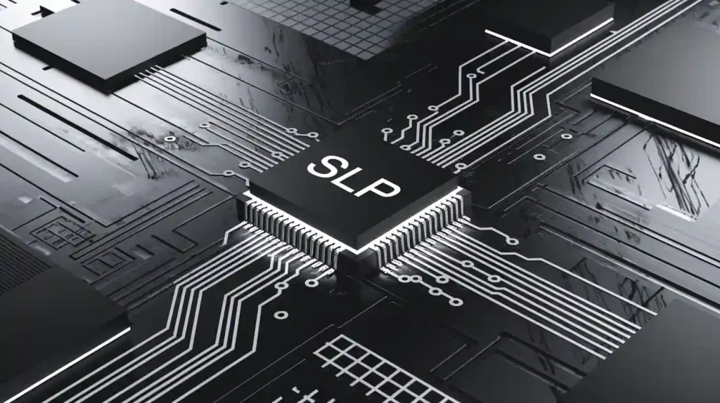
SLP-substrate like PCBs represent a cutting-edge innovation in printed circuit board technology. These advanced PCBs are engineered to meet the demands of high-density and high-performance applications. By enabling smaller designs without compromising functionality, they play a pivotal role in the miniaturization of modern electronics.
You’ll find substrate-like PCBs at the heart of devices like smartphones, wearables, and IoT sensors. Their compact structure allows manufacturers to integrate more features into smaller spaces, enhancing device capabilities. Industry reports predict rapid growth in multilayer PCBs and High-Density Interconnects (HDI) due to their reliability and adaptability in extreme environments, particularly in military and aerospace sectors. This trend underscores the transformative potential of SLP technology in shaping next-generation electronics.
Key Takeaways
- SLP-substrate like PCBs help create smaller, faster devices. They are important for modern gadgets like smartphones and IoT tools.
- These PCBs handle heat better and keep signals strong. This makes them reliable for fast-working devices.
- With SLPs, makers can use thinner lines and tighter spaces. This allows more parts to fit in small devices like wearables.
- SLP technology helps with new designs and better power use. It works well for future electronics in many industries.
- Even though they cost more to make, SLPs are worth it. They improve performance and make devices smaller, which is great for high-tech uses.
What Are SLP-Substrate Like PCBs?
Definition of Substrate-Like PCB
Substrate-like PCBs, often referred to as SLPs, represent a significant advancement in printed circuit board technology. These PCBs are designed to bridge the gap between traditional HDI (High-Density Interconnect) PCBs and IC substrates. By leveraging advanced manufacturing techniques, SLPs achieve finer line widths and spacing, enabling higher circuit density. This makes them ideal for applications where space is limited, such as smartphones, wearables, and IoT devices.
Unlike conventional PCBs, substrate-like PCBs utilize materials and processes that closely resemble those used in IC substrates. This allows them to deliver superior electrical performance, enhanced thermal management, and improved reliability. As a result, SLPs have become a cornerstone of modern electronics, driving innovation in compact and high-performance devices.
Note: The term “substrate-like” highlights the similarity of these PCBs to IC substrates, particularly in terms of their structure and manufacturing precision.
Key Differences Between SLP and Traditional PCBs
When comparing SLPs to traditional PCBs, several critical differences emerge. These differences stem from the materials used, the manufacturing processes, and the resulting performance characteristics. The table below highlights some of the key distinctions:
| Property | Traditional PCB (HDI) | Substrate-Like PCB (IC Substrate) |
|---|---|---|
| Dielectric Constant (Dk) | 4.2 – 4.5 (FR4) | 3.0 – 3.3 |
| Dissipation Factor (Df) | > 0.015 (FR4) | < 0.008 |
| Glass Transition Temperature (Tg) | 130 – 170°C (FR4) | > 210°C |
| Coefficient of Thermal Expansion (CTE) | 50 – 70 ppm/°C | < 45 ppm/°C |
These differences highlight why SLPs outperform traditional PCBs in high-frequency and high-temperature environments. For instance, the lower dielectric constant and dissipation factor of SLPs ensure better signal integrity, making them suitable for devices requiring high-speed data transmission. Additionally, their higher glass transition temperature and lower thermal expansion coefficient enhance durability and reliability, especially in compact and heat-sensitive applications.
You’ll also notice that SLPs achieve finer line widths and spacing, typically below 30 microns. This level of precision is unattainable with traditional PCB manufacturing methods. As a result, SLPs enable the integration of more components into smaller spaces, a critical requirement for modern electronics.
Tip: If you’re designing devices with stringent performance and size requirements, consider using substrate-like PCBs to achieve optimal results.
Why SLP-Substrate Like PCBs Matter
Applications in Consumer Electronics and IoT
SLP-substrate like PCBs have revolutionized the design and functionality of modern consumer electronics and IoT devices. You encounter these advanced PCBs in products like smartphones, smartwatches, fitness trackers, and IoT sensors. Their ability to support high-density component placement allows manufacturers to create smaller, more powerful devices that meet the growing demand for portability and performance.
In consumer electronics, SLPs enable features like multi-camera systems, advanced graphics processing, and extended battery life. For instance, the graphics card PCB in a smartphone relies on SLP technology to handle high-speed applications such as gaming and video streaming. Similarly, IoT devices benefit from the compact design of substrate-like PCBs, which integrate sensors, communication modules, and power management systems into a single, efficient package.
The precision manufacturing of SLPs ensures superior signal integrity considerations, which is critical for high-speed data transmission in IoT networks. Tools like Time Domain Reflectometry (TDR) and Vector Network Analyzers (VNA) validate the performance of these PCBs by measuring parameters such as impedance, reflection, and insertion loss. These benchmarks confirm their suitability for multi-Gbps channel assessments, ensuring reliable communication in connected devices.
Moreover, compliance with IPC standards like IPC-2226 and IPC-6016 guarantees consistent quality and performance in SLP fabrication. These guidelines outline design recommendations and performance metrics, ensuring that SLPs meet the rigorous demands of consumer electronics and IoT applications.
Benefits of SLP Technology in Modern Devices
SLP technology offers numerous advantages that make it indispensable in modern electronics. One of its most significant benefits is PCB miniaturization. By achieving finer line widths and spacing, typically below 30 microns, SLPs allow you to pack more functionality into smaller spaces. This capability is essential for devices like wearables, where compactness and performance go hand in hand.
Another key advantage is enhanced thermal management integration. SLPs use materials and processes similar to those in IC substrates, providing superior heat dissipation and reliability. This makes them ideal for high-density PCBs in devices that generate significant heat, such as graphics card PCBs and high-speed applications.
SLPs also excel in signal integrity considerations. Their lower dielectric constant and dissipation factor ensure minimal signal loss, making them perfect for high-speed data transmission. Automated Optical Inspection (AOI) and X-ray inspection during manufacturing verify the precision of line widths, spacing, and internal vias, ensuring optimal performance.
Power integrity is another area where SLPs shine. Techniques like decoupling capacitor modeling and voltage drop analysis help minimize voltage ripple and ground bounce, ensuring stable power delivery. These features are crucial for applications like core rail validation and transient analysis in advanced electronics.
Finally, SLP technology supports innovative designs by enabling complex component placement. This flexibility allows you to create devices with unique form factors and enhanced functionality, meeting the ever-evolving demands of the electronics market.
Tip: If you’re designing next-generation devices, consider SLP-substrate like PCBs for their unmatched combination of performance, reliability, and compactness.
How SLP-Substrate Like PCBs Are Made
Overview of the Manufacturing Process
The production of SLP-substrate like PCBs involves advanced techniques to achieve the precision required for high-density designs. You’ll notice that the process begins with selecting materials similar to those used in IC substrates. These materials ensure superior electrical performance and thermal stability. Manufacturers then use laser drilling to create microvias, enabling finer line widths and spacing. This step is critical for achieving the compact designs that modern devices demand.
Next, the circuit patterns are formed using semi-additive processes (SAP). This method allows for trace widths as small as 5–15µm, a significant improvement over traditional HDI PCBs, which typically range from 50–100µm. The table below highlights some key differences in manufacturing metrics:
| Feature | Typical HDI PCB Range | IC Substrate Typical Value |
|---|---|---|
| Line/Space | 50–100µm | 5–15µm |
| Dielectric Constant (Dk) | 3.5–4.2 | 3.0–3.6 |
| Glass Transition Temp (Tg) | 170–250°C | >210°C |
| Copper Weight | 0.5–1 oz per layer | <0.5 oz per layer |
After patterning, the layers are laminated together to form a multilayer structure. SLPs often feature 4–18 layers, depending on the application. Finally, rigorous testing, including Automated Optical Inspection (AOI) and X-ray inspection, ensures the PCB meets quality standards.
Challenges in SLP Production
Producing SLP-substrate like PCBs comes with unique challenges. Achieving the fine line widths and spacing required for these PCBs demands cutting-edge equipment and precise control over manufacturing parameters. For instance, maintaining trace widths as small as 5µm requires advanced lithography techniques and cleanroom environments to prevent contamination.
Thermal management poses another challenge. The materials used in SLPs must balance a low dielectric constant with high thermal stability. This balance ensures reliable performance in heat-sensitive applications like graphics card PCBs. Additionally, the lamination process for multilayer SLPs requires precise alignment to avoid defects that could compromise signal integrity.
Cost is another factor you must consider. The specialized materials and processes used in SLP production often result in higher manufacturing costs compared to traditional PCBs. However, the benefits—such as improved performance and miniaturization—often outweigh these costs in high-performance applications.
Despite these challenges, advancements in manufacturing technology continue to improve the efficiency and scalability of SLP production. As demand for compact, high-performance devices grows, you can expect further innovations in this field.
Future of SLP-Substrate Like PCBs
Emerging Trends in SLP Technology
SLP technology continues to evolve, driven by the demand for smaller, faster, and more efficient devices. You’ll notice that manufacturers are adopting advanced techniques like semi-additive processes (SAP) to achieve finer line widths and spacing. These innovations allow for greater circuit density, which is essential for compact designs in modern electronics.
Emerging materials also play a significant role in shaping the future of SLPs. High-performance substrates with lower dielectric constants and improved thermal stability are becoming standard. These materials enhance signal integrity and heat dissipation, making SLPs ideal for high-speed applications like graphics card PCBs.
Automation is another trend transforming SLP production. You’ll see increased use of AI-driven inspection systems to ensure precision in manufacturing. These systems detect defects in microvias and trace patterns, improving reliability and reducing production costs.
The integration of SLPs into flexible electronics is gaining traction as well. Flexible substrates enable unique form factors, opening doors to innovative designs in wearables and IoT devices. This trend highlights the versatility of SLP technology in meeting diverse application needs.
Impact of SLP on Next-Generation Electronics
SLP technology is set to redefine the capabilities of next-generation PCBs. By enabling PCB miniaturization, it allows you to design devices with unprecedented functionality in smaller spaces. This capability is crucial for industries like consumer electronics, where compactness drives innovation.
The impact of SLPs extends to high-performance computing. Their ability to support high-density component placement enhances the efficiency of graphics card PCBs and other advanced systems. You’ll find that SLPs improve signal integrity and power delivery, ensuring stable operation in demanding applications.
SLPs also pave the way for seamless integration with IC substrates. This synergy boosts performance in devices requiring high-speed data transmission and thermal management. As a result, SLPs are becoming indispensable in applications like 5G networks and autonomous vehicles.
The environmental benefits of SLP technology cannot be overlooked. By reducing material usage and enabling energy-efficient designs, SLPs contribute to sustainable manufacturing practices. This aligns with the growing emphasis on eco-friendly electronics in the global market.
As you look ahead, the role of SLPs in next-generation electronics will only expand. Their ability to combine compactness, reliability, and performance makes them a cornerstone of technological advancement.
SLP-substrate like PCBs represent a transformative leap in electronics, offering unmatched precision and performance. These advanced PCBs enable compact designs, making them essential for modern devices like smartphones, IoT sensors, and wearables. Their superior thermal management and signal integrity ensure reliability in high-performance applications.
You’ll see their impact across industries, from consumer electronics to aerospace and defense. The growing demand for high-performance electronics has spurred innovation, with nations investing in advanced military technology and additive manufacturing processes. These trends highlight the pivotal role of SLPs in driving technological progress.
Looking ahead, SLP technology will continue to revolutionize electronics. Its ability to combine miniaturization, efficiency, and sustainability positions it as a cornerstone of next-generation devices.
FAQ
1. What makes SLP-substrate like PCBs different from HDI PCBs?
SLP PCBs achieve finer line widths and spacing, typically below 30 microns, compared to HDI PCBs. They use advanced materials and processes similar to IC substrates, offering better signal integrity, thermal management, and reliability for compact, high-performance devices.
2. Can SLP PCBs be used in flexible electronics?
Yes, SLP technology integrates well with flexible substrates. This compatibility enables unique form factors for wearables and IoT devices, allowing you to design innovative products that combine flexibility, compactness, and high performance.
3. Are SLP PCBs more expensive to manufacture?
SLP PCBs cost more due to specialized materials and precision manufacturing techniques. However, their benefits—such as miniaturization, enhanced performance, and reliability—make them a worthwhile investment for high-performance applications.
4. What industries benefit most from SLP PCBs?
SLP PCBs are widely used in consumer electronics, IoT, aerospace, and defense. Their compact design and superior performance make them ideal for smartphones, wearables, autonomous vehicles, and military-grade systems.
5. How do SLP PCBs improve signal integrity?
SLP PCBs use materials with lower dielectric constants and dissipation factors. These properties minimize signal loss and ensure high-speed data transmission, making them suitable for applications like 5G networks and advanced computing systems.


