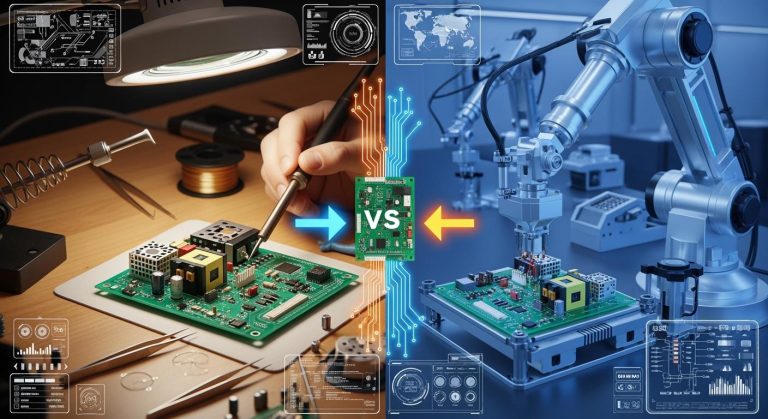
Steps to Master Surface Mount PCB Assembly
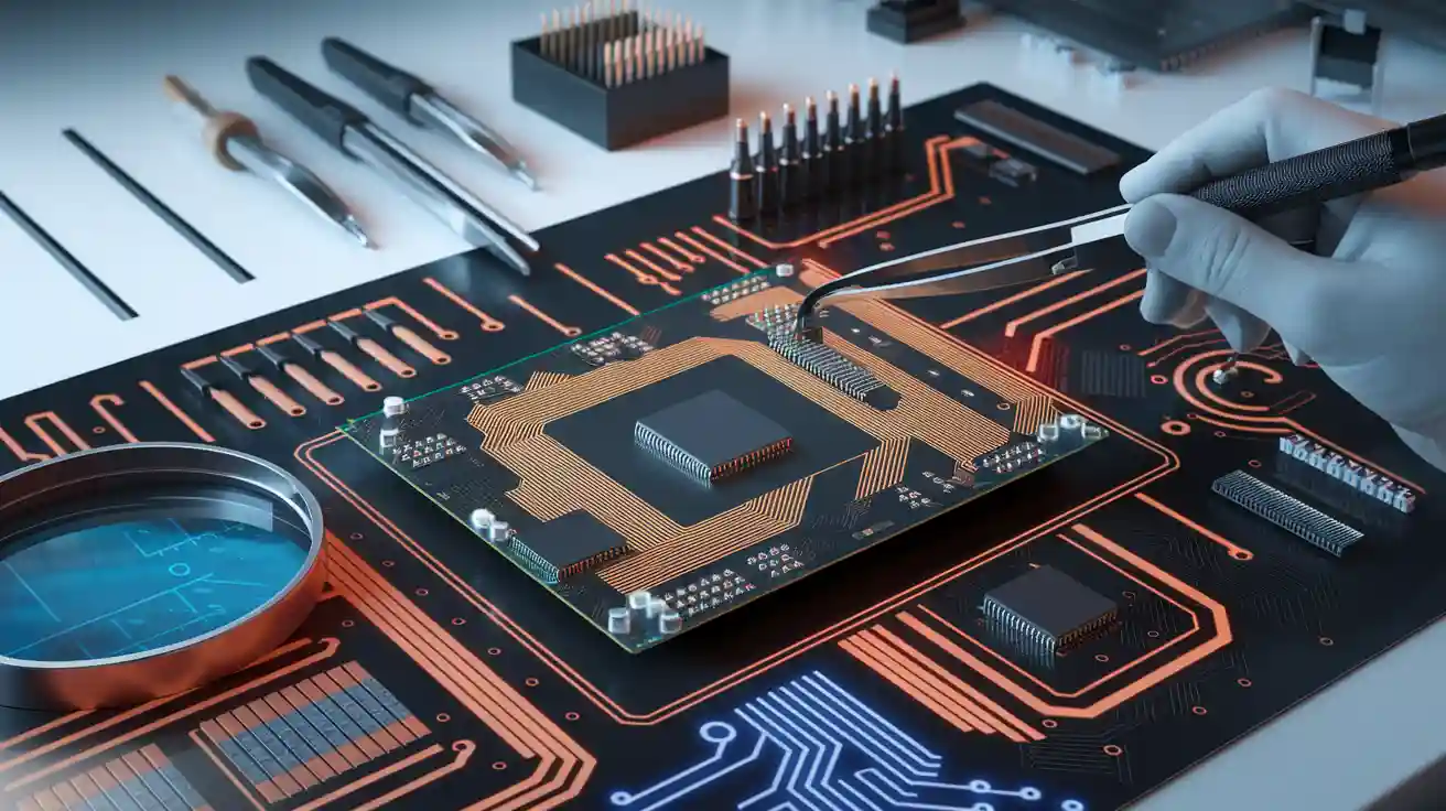
In my experience, surface mount PCB assembly demands an exceptional level of precision and reliability. Every step in the process must align with the highest standards to ensure functional and durable PCBs. For instance, solder paste application requires precise alignment with PCB pads to create strong solder joints, especially for fine-pitch components. Automated part placement systems achieve micron-level accuracy and verify orientation through advanced vision systems. After assembly, Automated Optical Inspection (AOI) scans the PCB to identify any soldering or placement errors, which is critical for high-density designs. Mastering these steps ensures a seamless and efficient assembly process.
Key Takeaways
- Learn how PCB design and layout work. This helps you avoid problems and make sure the PCB works as planned.
- Use good tools and materials. Tools like sharp tweezers and strong solder paste make the PCB better.
- Keep your workspace neat and bright. A clean area helps you work faster and make fewer mistakes.
- Check the Bill of Materials (BOM) and instructions closely. This step stops delays and helps you put parts in the right spots.
- Test and inspect often. Finding problems early with tools like AOI makes the PCB more reliable.
Preparation and Planning
Understanding PCB design and layout
Before starting any printed circuit board assembly, I always emphasize the importance of thoroughly understanding the PCB design and layout. A well-designed PCB acts as the foundation for a successful assembly process. I carefully review the schematic diagrams and layout files to identify critical components, signal paths, and power distribution networks. This step helps me anticipate potential challenges, such as thermal management or high-frequency signal interference. By analyzing the design, I ensure that the assembly process aligns with the intended functionality of the PCB.
Gathering tools and materials for PCBA
Using high-quality tools and materials is non-negotiable in surface mount PCB assembly. I always ensure that my toolkit includes precision tweezers, soldering irons with adjustable temperature controls, and a reliable solder paste dispenser. For materials, I prioritize those that enhance the mechanical and electrical properties of the PCB. For instance, functionalized g-C₃N₄ nanofillers significantly improve the mechanical reliability of PCBs. These materials offer tensile strength of 192.4 MPa, flexural strength of 315.4 MPa, and impact strength of 6.3 J, outperforming traditional FR-4 PCBs. Such enhancements are crucial for ensuring the durability and performance of the final product.
Organizing workspace for surface mount PCB assembly
An organized workspace is essential for efficient and error-free assembly. I arrange my tools and materials systematically, ensuring that everything I need is within easy reach. Proper lighting is another critical factor; I use adjustable LED lamps to illuminate the workspace and reduce eye strain. To maintain cleanliness, I use anti-static mats and wrist straps to prevent electrostatic discharge, which can damage sensitive components. A clutter-free and well-lit environment not only improves productivity but also minimizes the risk of mistakes during the assembly process.
Reviewing BOM and assembly instructions
Before starting the assembly process, I always dedicate time to thoroughly reviewing the Bill of Materials (BOM) and assembly instructions. This step is critical for ensuring a smooth and error-free workflow. The BOM acts as the blueprint for component selection, listing part numbers, values, and package types. By cross-referencing this information with the assembly instructions, I confirm that the correct components are used and placed in their designated positions.
A clean and complete BOM streamlines procurement and eliminates confusion during assembly. For example, I’ve seen how a well-prepared BOM prevents costly delays caused by missing or incorrect parts. It also ensures that every component aligns with the design specifications, reducing the likelihood of assembly errors. This meticulous approach not only saves time but also enhances the overall quality of the final product.
Tip: Always verify the BOM against the PCB layout to catch discrepancies early. This proactive step can significantly improve yields and minimize rework.
In addition to the BOM, I carefully analyze the assembly instructions. These documents often include critical details, such as polarity markings, placement orientations, and soldering guidelines. Following these instructions precisely ensures that components are installed correctly and function as intended. I also incorporate Design for Manufacturing (DFM) feedback during this stage. DFM reviews highlight potential issues, such as tight tolerances or inaccessible solder joints, allowing me to address them before assembly begins.
By prioritizing this review process, I’ve consistently minimized errors and improved efficiency in surface mount PCB assembly. It’s a step I never skip, as it lays the foundation for a successful build.
Step-by-Step Assembly Process
Solder paste printing techniques
Solder paste printing is the foundation of the surface mount PCB assembly process. I use a stencil to apply solder paste onto the PCB pads with precision. The stencil design plays a critical role in ensuring even deposition. I always ensure the stencil apertures match the pad dimensions to achieve accurate solder paste application. Close contact between the stencil and PCB during printing is essential for high-quality results.
Automated solder paste printing systems enhance efficiency by maintaining consistent pressure and alignment. These systems ensure the paste is applied uniformly, which is crucial for effective soldering during reflow. The precision of solder paste application directly impacts the reliability of the assembly. For example:
- The stencil ensures even and precise deposition of solder paste onto the pads.
- Automated placement of components and reflow soldering enhance the overall automation and efficiency of the process.
- The design of stencil apertures influences the accuracy of solder paste application.
Tip: Regularly inspect the stencil for wear and tear. A damaged stencil can lead to uneven paste application, causing defects in the final assembly.
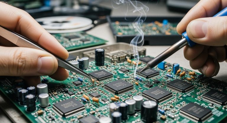
SMT component placement methods
After applying solder paste, the next step is placing components onto the PCB. I rely on pick-and-place machines for this task. These machines use advanced vision systems to identify component orientation and ensure accurate placement. The precision of these systems is critical for high-density designs, where components are closely packed.
To verify the reliability of SMT component placement methods, I incorporate quality assurance techniques such as:
- In-circuit testing (ICT) to check if components are working and properly connected.
- Boundary scan testing for chips and boards without using test pins.
- Functional testing to ensure the board works as expected in real-world applications.
Manual placement may be necessary for unique or irregular components. In such cases, I use precision tweezers and follow the assembly instructions carefully to avoid misalignment. Proper placement of components ensures they remain secure during the reflow soldering process.
Note: Always calibrate pick-and-place machines regularly to maintain accuracy and prevent errors during the assembly process.
Reflow soldering process
Reflow soldering is the final step in the surface mount PCB assembly process. This stage involves heating the PCB to melt the solder paste and create strong solder joints. I use a reflow oven with controlled temperature profiles to ensure optimal results. The heating profile includes preheat, soak, and reflow stages, each tailored to the solder paste and component specifications.
Controlled experiments have shown that the volume of solder paste significantly influences the retention of ball alloy in the joint after reflow. For specific combinations of ball and paste alloys, the amount of paste deposited directly affects how much ball alloy is consumed during the reflow process. This relationship is critical for optimizing the reflow soldering process to ensure reliability in mass production.
During reflow, I monitor the thermal stress on components to prevent damage. Proper cooling after reflow solidifies the solder joints and ensures the PCB is ready for inspection. By maintaining precise control over the reflow parameters, I consistently achieve high-quality results in surface mount PCB assembly.
Tip: Use thermal profiling tools to measure the temperature across the PCB during reflow. This ensures uniform heating and prevents defects caused by uneven soldering.
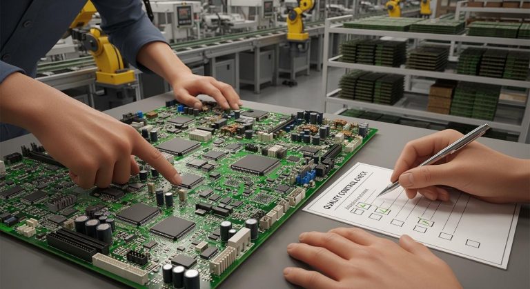
Inspection and testing procedures
Inspection and testing are critical steps in the PCB assembly process. They ensure that the final product meets quality standards and functions as intended. I always prioritize these procedures to identify and address potential defects early, which saves time and resources.
The first step in my inspection routine involves solder paste inspection. This process verifies the accuracy of solder paste application on the PCB pads. I use automated solder paste inspection systems to measure paste volume, height, and alignment. These systems provide detailed feedback, allowing me to make adjustments before component placement. Consistent solder paste application is essential for creating reliable solder joints during reflow.
After solder paste inspection, I conduct a thorough examination of component placement. Automated Optical Inspection (AOI) systems play a vital role here. These systems use high-resolution cameras to detect misaligned or missing components. For high-density designs, I rely on 3D AOI systems, which provide a more comprehensive view of the PCB. This technology ensures that every component is correctly positioned before soldering.
Functional testing is another essential part of my process. It evaluates whether the assembled PCB performs as expected under real-world conditions. For example, I use in-circuit testing to check electrical connections and boundary scan testing for inaccessible areas. These methods help me verify the integrity of the assembly and identify any issues that require correction.
In one notable case, an automotive electronics manufacturer discovered micro-voids in solder joints using high-resolution 3D X-Ray inspection. These voids caused failures in Engine Control Units (ECUs), leading to costly recalls. By implementing advanced inspection techniques, the company improved its SMT process and avoided further issues. This example highlights the importance of thorough inspection in preventing field failures.
Tip: Early inspections can identify defects promptly, preventing flawed products from advancing in the assembly process. This proactive approach increases the final yield rate and mitigates financial losses from recalls.
Cleaning and finishing the PCB
Once the inspection and testing procedures are complete, I move on to cleaning and finishing the PCB. This step ensures that the final product is free from contaminants and ready for deployment.
Cleaning the PCB is crucial for removing residues left behind during the assembly process. Solder flux residues, for instance, can cause corrosion or electrical leakage if not properly cleaned. I use ultrasonic cleaning systems for this task. These systems generate high-frequency sound waves that create microscopic bubbles, effectively removing contaminants from the PCB surface. For no-clean solder pastes, I still perform a light cleaning to ensure optimal performance.
After cleaning, I inspect the PCB again to confirm that no residues remain. I use magnification tools to examine hard-to-reach areas, such as under components. This step guarantees that the PCB meets cleanliness standards and is free from any potential issues.
The finishing process involves applying protective coatings to enhance the PCB’s durability. I use conformal coatings to shield the PCB from moisture, dust, and chemical exposure. These coatings also improve the mechanical strength of the assembly, ensuring long-term reliability. For high-frequency applications, I select coatings with low dielectric constants to minimize signal interference.
Finally, I package the PCB to protect it during transportation and storage. I use anti-static bags and foam inserts to prevent physical damage and electrostatic discharge. Proper packaging ensures that the PCB reaches its destination in perfect condition.
Note: Always verify the compatibility of cleaning agents and coatings with the PCB materials to avoid unintended damage.
By following these cleaning and finishing procedures, I ensure that the PCB is not only functional but also robust and ready for its intended application.
Common Challenges and Solutions
Preventing soldering defects
Soldering defects remain one of the most common challenges in surface mount PCB assembly. These defects, such as cold joints, solder bridging, and voids, can compromise the electrical performance and reliability of the PCB. Over the years, I’ve developed a systematic approach to minimize these issues.
The first step involves optimizing the reflow oven profiles. I adjust the conveyor speed and zone temperatures in small increments, typically 5°C, during testing. This ensures the solder paste melts uniformly, eliminating cold joints or solder beading. Additionally, I prioritize stencil design. Using laser-cut stainless-steel stencils with aperture sizes matching the pad dimensions ensures precise solder paste deposition. For fine-pitch components, I reduce the aperture size slightly to prevent solder bridging.
Component placement accuracy also plays a critical role. I ensure pick-and-place machines achieve a placement accuracy of ±25μm for small components. Machine vision systems with fiducial markers help correct positional drift, ensuring components align perfectly with the PCB pads. Selecting the right solder paste is equally important. For high-density boards, I use Type 3 or Type 4 solder pastes with no-clean fluxes. These pastes leave minimal residue, reducing the risk of ionic contamination.
Preheating the PCB before soldering is another effective method. I precondition bare boards at 80–100°C for about 30 minutes. This step drives off moisture and reduces the risk of warpage during reflow. Lastly, I emphasize operator training. Monthly sessions on defect recognition using annotated samples help my team identify and address potential issues early.
| Method | Implementation |
|---|---|
| Adjust Reflow Oven Profiles | Test conveyor speed and zone temperatures in 5°C increments to eliminate defects. |
| Stencil Design Best Practices | Use laser-cut stencils with aperture sizes 1:1 to pad dimensions. |
| Control Component Placement | Ensure ±25μm accuracy with machine vision and fiducial markers. |
| Select Suitable Solder Paste | Use Type 3 or Type 4 pastes with no-clean fluxes for high-density boards. |
| Preheat PCBs | Precondition boards at 80–100°C for 30 minutes to reduce warpage. |
Tip: Regularly calibrate equipment and inspect stencils for wear. These proactive measures prevent soldering defects and improve assembly quality.
Correcting component misalignment
Component misalignment can disrupt the functionality of a PCB and lead to costly rework. I’ve encountered this issue frequently, especially in high-density assemblies where components are closely packed. To address this, I rely on a combination of advanced tools and meticulous processes.
Pick-and-place machines are my primary solution for ensuring accurate component placement. These machines use high-resolution cameras and fiducial markers to align components with the PCB pads. I calibrate these machines regularly to maintain their accuracy. For unique or irregular components that require manual placement, I use precision tweezers and follow the assembly instructions carefully.
Inspection is another critical step. Automated Optical Inspection (AOI) systems help me detect misaligned components early in the process. For complex designs, I use 3D AOI systems, which provide a detailed view of the PCB and highlight any alignment issues. Functional testing further verifies that all components are correctly positioned and connected.
In cases where misalignment occurs, I take immediate corrective action. For minor shifts, I use rework stations to adjust the component position. For more significant issues, I remove the component, clean the pad, and reapply solder paste before reattaching it. This ensures the integrity of the assembly and prevents future failures.
Note: Always verify the alignment of components during the first article inspection. Early detection minimizes rework and ensures a smoother assembly process.
Managing thermal stress during reflow soldering
Thermal stress during reflow soldering poses a significant challenge, especially for sensitive components. Excessive stress can lead to solder joint failures, warpage, or even component damage. I’ve found that managing thermal profiles effectively is the key to mitigating these risks.
The reflow process involves heating the PCB through several stages, including preheat, soak, and reflow. I use thermal profiling tools to measure the temperature across the PCB and ensure uniform heating. This prevents localized overheating, which can cause thermal stress. Preheating the PCB also helps. By gradually raising the temperature, I reduce the risk of thermal shock and improve solder joint reliability.
Research highlights the importance of optimizing solder joint design to manage thermal stress. For example, cylindrical solder joints have been shown to lower peak equivalent stress, enhancing reliability in applications like photonic sensing. I incorporate these findings into my designs to improve the durability of the assembly.
Cooling is another critical aspect. After the reflow stage, I ensure the PCB cools down gradually to avoid introducing additional stress. Controlled cooling solidifies the solder joints and stabilizes the assembly. For high-reliability applications, I also conduct thermal cycling tests to evaluate the PCB’s performance under varying temperature conditions.
Tip: Use reflow ovens with multiple heating zones to fine-tune the thermal profile. This ensures each component experiences the optimal temperature range during soldering.
By addressing these challenges systematically, I’ve consistently improved the quality and reliability of my PCB assemblies. These strategies not only prevent defects but also enhance the overall efficiency of the assembly process.
Enhancing inspection accuracy
Inspection accuracy plays a pivotal role in ensuring the quality and reliability of surface mount PCB assemblies. Over the years, I’ve refined my approach to inspection by integrating advanced tools and techniques that minimize errors and enhance efficiency. Below, I’ll share the strategies I use to achieve precise and reliable inspections.
Leveraging Automated Optical Inspection (AOI) Systems
Automated Optical Inspection (AOI) systems are indispensable for detecting defects in component placement and solder joints. I rely on high-resolution 2D and 3D AOI systems to identify issues such as misaligned components, solder bridging, and insufficient solder coverage. These systems use advanced algorithms to analyze the PCB and highlight discrepancies.
For high-density designs, I prefer 3D AOI systems. They provide a detailed view of the PCB, allowing me to inspect solder joints from multiple angles. This capability is especially useful for identifying micro-voids or hidden defects that traditional 2D systems might miss.
Tip: Regularly calibrate AOI systems to maintain their accuracy. Calibration ensures consistent detection of defects and reduces false positives.
Implementing X-Ray Inspection
X-ray inspection is another powerful tool I use to enhance accuracy. It allows me to examine solder joints and components that are hidden beneath the surface, such as Ball Grid Arrays (BGAs) and Quad Flat No-lead (QFN) packages. By analyzing the internal structure of these components, I can detect voids, cracks, or other anomalies that might compromise the PCB’s performance.
I’ve found that combining X-ray inspection with AOI provides a comprehensive view of the assembly. While AOI excels at surface-level inspections, X-ray systems reveal hidden defects, ensuring no issue goes unnoticed.
Establishing Inspection Checkpoints
To streamline the inspection process, I establish multiple checkpoints throughout the assembly workflow. These checkpoints include:
- Pre-solder inspection: Verifying solder paste application and component placement before reflow.
- Post-reflow inspection: Examining solder joints and component alignment after soldering.
- Final inspection: Conducting functional tests to ensure the PCB meets design specifications.
By breaking the inspection process into stages, I can identify and address defects early, reducing the need for rework and improving overall efficiency.
Training and Skill Development
Inspection accuracy isn’t solely dependent on tools; it also requires skilled operators. I invest in regular training sessions for my team to ensure they understand the latest inspection techniques and technologies. These sessions include hands-on practice with AOI and X-ray systems, as well as defect recognition exercises using annotated samples.
Note: Skilled operators can identify subtle defects that automated systems might overlook. Their expertise complements the capabilities of inspection tools, creating a robust quality control process.
Using Statistical Process Control (SPC)
Statistical Process Control (SPC) helps me monitor and improve inspection accuracy over time. By analyzing data from inspection systems, I can identify trends and patterns that indicate recurring issues. For example, if solder bridging occurs frequently in a specific area of the PCB, I investigate the root cause and implement corrective measures.
| Inspection Tool | Strengths | Applications |
|---|---|---|
| AOI Systems | Surface-level defect detection | Component placement, solder joints |
| X-Ray Systems | Internal defect detection | BGAs, QFNs, hidden solder joints |
| SPC | Process optimization | Identifying trends, improving yields |
By combining advanced tools, systematic processes, and skilled personnel, I consistently achieve high inspection accuracy in surface mount PCB assembly. This approach not only ensures the quality of the final product but also enhances customer satisfaction and trust in my work.
Modern Trends and Best Practices

Automation in surface mount PCB assembly
Automation has revolutionized surface mount PCB assembly, making processes faster and more reliable. I’ve seen how automated systems, such as pick-and-place machines and reflow ovens, streamline workflows and reduce human error. These machines use advanced algorithms and vision systems to ensure precise component placement and soldering. For example, digital twin technology allows me to simulate the assembly process virtually, identifying potential issues before production begins. This proactive approach minimizes defects and enhances efficiency.
Artificial intelligence (AI) plays a significant role in modern automation. AI-powered inspection systems analyze PCBs in real-time, detecting defects with unparalleled accuracy. These systems adapt to new designs and learn from previous inspections, improving their performance over time. By integrating AI into my workflow, I’ve reduced inspection times and improved overall quality.
Advanced soldering techniques for PCBA
Soldering techniques have evolved significantly, enabling better performance and reliability in PCBA. I’ve adopted methods like selective soldering and laser soldering to handle complex designs and sensitive components. Selective soldering targets specific areas of the PCB, reducing thermal stress on nearby components. Laser soldering, on the other hand, offers pinpoint accuracy, making it ideal for high-density assemblies.
Lead-free soldering has become a standard practice due to environmental regulations. I use lead-free solder alloys, such as SAC305, which provide excellent mechanical strength and thermal conductivity. These materials align with green manufacturing requirements, ensuring compliance without compromising quality.
Thermal profiling remains critical in advanced soldering. I use profiling tools to monitor temperature across the PCB during reflow, ensuring uniform heating. This technique prevents defects like cold joints and solder bridging, improving the reliability of the final assembly.
Quality control and testing standards
Quality control is the backbone of successful PCB assembly. I follow stringent testing standards to ensure every PCB meets design specifications. Automated Optical Inspection (AOI) and X-ray systems are integral to my process. AOI systems detect surface-level defects, while X-ray systems reveal hidden issues in solder joints and components. Combining these methods provides comprehensive inspection coverage.
Statistical Process Control (SPC) has transformed how I monitor quality. Real-time data analysis helps me identify trends and prevent defects before they occur. For instance, if solder bridging becomes frequent in a specific area, SPC data pinpoints the root cause, allowing me to implement corrective measures.
Green manufacturing practices also influence quality standards. I prioritize energy-efficient processes and lead-free materials, aligning with industry trends while maintaining high-quality output. These practices not only enhance reliability but also demonstrate a commitment to sustainability.
| Trend | Description |
|---|---|
| High-Density Interconnect (HDI) | Finer lines (<50μm), Microvia technology |
| Flexible Electronics Manufacturing | Flexible substrate assembly, 3D curved surfaces |
| Smart Manufacturing Transformation | Digital twin applications, AI-powered inspection |
| Green Manufacturing Requirements | Lead-free materials, energy-efficient processes |
| Quality Inspection | Multiple methods including AOI and X-ray |
| Statistical Process Control (SPC) | Real-time data monitoring to prevent defects |
By embracing these modern trends and best practices, I’ve consistently improved the efficiency and reliability of my PCB assembly processes. These advancements not only enhance product quality but also position me at the forefront of industry innovation.
Adopting industry standards for PCB assembly
Adopting industry standards in PCB assembly has been a cornerstone of my approach to ensuring quality and reliability. These standards provide a framework that aligns manufacturing processes with global benchmarks, reducing errors and improving consistency. By following these guidelines, I’ve been able to streamline workflows and meet customer expectations more effectively.
Key Industry Standards I Follow
- IPC-A-610: This standard defines the acceptability criteria for electronic assemblies. It serves as my go-to reference for evaluating solder joints, component placement, and overall assembly quality.
- ISO 9001: This quality management standard helps me maintain a systematic approach to process improvement. It ensures that every step in the assembly process meets rigorous quality requirements.
- RoHS Compliance: Restriction of Hazardous Substances (RoHS) compliance is critical for environmentally friendly manufacturing. I use lead-free solder and other compliant materials to meet these regulations.
- J-STD-001: This standard outlines the requirements for soldered electrical and electronic assemblies. It provides detailed guidance on materials, methods, and acceptance criteria.
Tip: Familiarize yourself with these standards early in the design phase. Doing so minimizes rework and ensures compliance throughout the assembly process.
Benefits of Adopting Standards
Adhering to industry standards has transformed my assembly processes. It has improved product reliability, reduced defect rates, and enhanced customer satisfaction. For instance, IPC-A-610 guidelines have helped me identify and rectify soldering defects before they escalate. ISO 9001 has streamlined my documentation and quality control procedures, making audits more efficient.
| Standard | Focus Area | Key Benefit |
|---|---|---|
| IPC-A-610 | Assembly quality | Reduces defects |
| ISO 9001 | Quality management | Streamlines processes |
| RoHS Compliance | Environmental safety | Ensures eco-friendly manufacturing |
| J-STD-001 | Soldering requirements | Improves solder joint reliability |
By integrating these standards into my workflow, I’ve not only met regulatory requirements but also gained a competitive edge. They serve as a roadmap for achieving excellence in surface mount PCB assembly.
Mastering surface mount PCB assembly requires a commitment to precision, planning, and continuous improvement. Each step, from solder paste application to inspection, builds the foundation for reliable and high-performing PCBs. I’ve seen how Statistical Process Control (SPC) stabilizes processes and prevents batch defects by utilizing real-time inspection data. Failure Mode and Effects Analysis (FMEA) optimizes test plans, addressing over 90% of potential failure modes.
By embracing modern trends like automation and advanced soldering techniques, I’ve consistently improved efficiency and quality. Industry standards further ensure consistency and reliability. Continuous learning and adaptation remain key to staying ahead in this dynamic field.
Tip: Always prioritize precision and planning to minimize errors and maximize yields in surface mount PCB assembly.
FAQ
What is the difference between SMT and THT in PCB assembly?
Surface Mount Technology (SMT) places components directly onto PCB pads, while Through-Hole Technology (THT) inserts components into drilled holes. SMT is ideal for compact designs, whereas THT offers stronger mechanical bonds for high-stress applications.
How can I prevent solder bridging during assembly?
I use laser-cut stencils with precise aperture sizes and optimize solder paste volume. Regular stencil inspections and controlled reflow profiles also help prevent solder bridging, ensuring clean and reliable joints.
What tools are essential for surface mount PCB assembly?
I rely on pick-and-place machines, reflow ovens, solder paste dispensers, and AOI systems. For manual tasks, precision tweezers, anti-static mats, and magnification tools are indispensable for achieving accuracy.
Why is thermal profiling important in reflow soldering?
Thermal profiling ensures uniform heating across the PCB, preventing defects like cold joints or component damage. I use profiling tools to monitor temperature zones and optimize the reflow process for reliability.
How do I clean PCBs after assembly?
I use ultrasonic cleaning systems to remove flux residues and contaminants. For no-clean solder pastes, I perform light cleaning to ensure optimal performance. Protective coatings enhance durability and shield the PCB from environmental factors.