How to apply PCB Layout RS 485 to signal control system
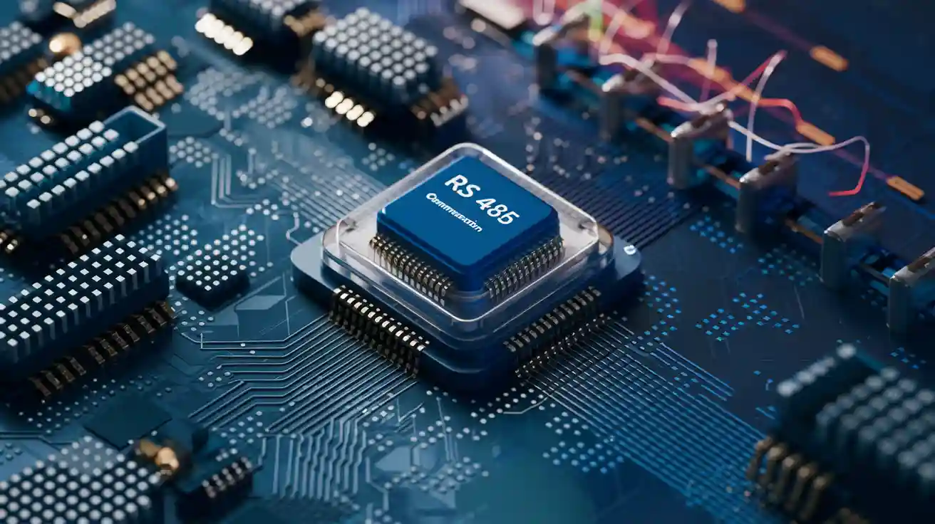
The RS 485 standard has become a cornerstone in industrial and control systems due to its robust communication capabilities. Its differential signaling method ensures consistent performance, even in electrically noisy environments. To fully leverage the RS 485 interface, you must focus on an optimized PCB layout. This approach enhances signal integrity, minimizes noise, and ensures reliable system operation.
For example, the MAXM22511 module demonstrates the impact of proper PCB design for RS 485 applications. It meets CISPR 11 requirements for EMI performance, showcasing its ability to handle high-frequency noise. Comparative testing also reveals its superior reliability against competitors, reinforcing the value of precise PCB layout techniques for RS 485 communication.
By mastering these principles, you can create systems that excel in durability and efficiency.
Key Takeaways
- Design RS485 traces as paired lines. This lowers noise and keeps signals clear.
- Add resistors at both ends of the RS485 network. These stop signal bouncing and keep communication steady.
- Use good grounding and shielding methods. This cuts down interference and makes the system more reliable.
- Place the RS485 chip near the connectors. This shortens the lines and avoids signal problems.
- Test the PCB layout with simulation tools. Testing finds issues early and ensures it works well.
Understanding RS485 in Signal Control Systems
Key Features of RS485
RS485 stands out as a reliable serial communication standard for industrial and control systems. Its key features make it ideal for demanding environments. For instance, it supports long cable runs up to 1,200 meters, making it suitable for large-scale installations. It also allows up to 32 devices to connect on a single network without repeaters, simplifying system design.
The protocol uses differential signaling, which ensures robust data transmission even in noisy environments. RS485 achieves data rates of up to 10 Mbps over short distances, while maintaining reliable communication at lower speeds over longer distances. Additionally, its common mode voltage range of -7V to +12V enhances compatibility with various devices. These features make RS485 a versatile choice for modern control systems.
| Feature | Specification |
|---|---|
| Maximum Cable Length | Up to 1200 meters |
| Maximum Data Rates | 10 Mbps (short distances) |
| Differential Voltage Levels | Minimum 200 mV |
| Maximum Number of Nodes | Up to 32 |
Differential Signaling and Noise Immunity
Differential signaling is a core principle of RS485. It transmits signals as the voltage difference between two wires, reducing the impact of electrical noise. This design ensures reliable data transmission, even in harsh industrial environments. Twisted-pair cables further enhance noise immunity by canceling out electromagnetic interference.
This approach minimizes signal degradation and improves resistance to interference over long distances. For example, RS485 communication remains stable in environments with high electrical noise, such as factories or power plants. By using differential signaling, you can achieve consistent performance and maintain signal integrity in your PCB designs.
Applications of RS485 in Industrial Systems
RS485 has a wide range of applications in industrial systems. It is commonly used in industrial automation for communication between PLCs, sensors, and actuators. Its ability to connect multiple devices on a single network reduces installation costs and simplifies system management.
In access control systems, RS485 enables secure communication between devices like card readers and controllers. It also plays a vital role in solar power systems, connecting inverters and monitoring devices while benefiting from its noise immunity. Additionally, RS485 supports long-distance communication, making it ideal for dispersed locations such as oil refineries or water treatment plants.
- Industrial Automation: Communication between PLCs and sensors.
- Access Control Systems: Secure device communication.
- Solar Power Systems: Reliable connections for monitoring devices.
- Long-Distance Communication: Effective up to 1,200 meters.
- Multi-Drop Networks: Supports up to 32 devices on a single bus.
PCB Layout Considerations for RS485
Trace Routing and Differential Pair Design
Proper trace routing is critical for maintaining the integrity of RS485 communication. You should prioritize differential pair design when routing traces for RS485 signals. Differential signaling relies on two complementary traces to transmit data, which minimizes noise and ensures reliable transmission. To achieve this, keep the traces of the differential pair close together and maintain consistent spacing throughout the PCB layout. This reduces electromagnetic interference and improves signal quality.
When routing traces, avoid sharp angles or abrupt changes in direction. These can cause signal reflections and degrade the performance of the RS485 protocol. Instead, use smooth curves or 45-degree angles to maintain signal integrity. Additionally, ensure that the traces are of equal length to prevent skewing, which can disrupt the timing of the differential signals.
For best practices, follow these benchmarks:
- Use twisted-pair cables for external connections to enhance noise immunity.
- Minimize the length of traces to reduce signal attenuation.
- Avoid crossing differential pairs with other signal traces to prevent crosstalk.
Impedance Matching for RS485 Communication
Impedance matching plays a vital role in optimizing RS485 communication. The RS485 protocol requires a characteristic impedance of 120 ohms for the transmission line. Matching the impedance of the PCB traces to this value ensures minimal signal reflection and maximizes data integrity. You can achieve this by carefully designing the trace width and spacing based on the PCB’s dielectric constant.
Termination resistors are essential for impedance matching. Place a 120-ohm resistor at each end of the RS485 network to match the line impedance. This prevents signal reflections and ensures stable communication. For multi-drop networks, use termination resistors only at the two endpoints to avoid overloading the network.
Simulation tools can help verify impedance matching during the design phase. These tools allow you to test the PCB layout and identify potential issues before manufacturing. By implementing impedance matching, you enhance the reliability of RS485 communication and reduce the risk of corrupted data packets.
Grounding and Shielding Techniques
Effective grounding and shielding techniques are crucial for reducing noise and ensuring stable RS485 communication. Grounding prevents ground-related issues, while shielding minimizes electromagnetic interference. To optimize grounding, check the device data sheets for specific recommendations. Isolate analog ground (AGND) and digital ground (DGND) planes on multilayer PCBs to prevent noisy digital currents from affecting sensitive analog circuitry.
Tie AGND and DGND pins to their respective ground planes to maintain isolation. Ensure that all layers of the PCB implement this isolation. For shielding, use edge guarding to reflect noise back into the interplane space. This technique reduces radiated emissions and improves signal integrity. Interplane capacitance bypassing further enhances noise reduction, especially at high frequencies between 200 MHz and 1 GHz.
The following table summarizes efficient grounding and shielding techniques:
| Technique | Description |
|---|---|
| Edge Guarding | Reflects noise back into the interplane space, reducing edge radiation. |
| Interplane Capacitance Bypassing | Improves bypass integrity at high frequencies, reducing conducted and radiated emissions. |
| Stitching Capacitance | Minimizes emissions across the spectrum, especially with low inductance. |
By implementing these techniques, you can create a robust PCB layout that supports reliable RS485 communication in noisy environments.
Component Placement for RS485 Transceivers
Placing the RS485 transceiver correctly on your PCB is essential for achieving reliable communication and maintaining signal integrity. The transceiver acts as the interface between the differential RS485 signals and your system’s logic circuitry. A well-thought-out placement strategy minimizes noise, reduces signal distortion, and ensures efficient data transmission.
1. Positioning the RS485 Transceiver Near Connectors
Place the RS485 transceiver as close as possible to the connector that interfaces with the external RS485 network. This minimizes the trace length for the differential signal pair, reducing the chances of signal degradation or electromagnetic interference. Shorter traces also help maintain the characteristic impedance of the transmission line, which is critical for stable RS485 communication.
2. Avoiding Crosstalk and Noise Sources
Keep the transceiver away from high-frequency components or noisy power supply circuits. Noise from these sources can couple into the differential signal traces, leading to data errors. Maintain a clear separation between the RS485 transceiver and other high-speed or high-power components on the PCB. Use ground planes to shield the transceiver from noise and improve overall signal integrity.
3. Optimizing Ground Connections
Ensure the transceiver’s ground pin connects directly to the PCB’s ground plane. A solid ground connection reduces noise and enhances the stability of the RS485 communication. Avoid using long or narrow ground traces, as these can introduce resistance and inductance, which degrade the performance of the transceiver.
4. Aligning with Differential Pair Traces
Align the transceiver’s input and output pins with the differential pair traces on the PCB. This alignment minimizes the need for sharp bends or long trace runs, which can cause signal reflections and timing issues. Maintain consistent spacing between the differential traces as they connect to the transceiver to preserve the impedance matching.
5. Thermal Management Considerations
RS485 transceivers can generate heat during operation, especially in high-speed or high-load applications. Place the transceiver in a location that allows for proper heat dissipation. If necessary, include thermal vias or copper pours around the transceiver to manage heat effectively.
6. Decoupling Capacitors Placement
Place decoupling capacitors as close as possible to the transceiver’s power supply pins. These capacitors filter out noise from the power supply and ensure stable operation. Use low-ESR capacitors for better performance, and connect them directly to the ground plane to minimize parasitic inductance.
By following these placement guidelines, you can optimize the performance of your RS485 transceiver and ensure reliable serial communication. Proper placement not only enhances signal quality but also simplifies the overall PCB layout, making your design more robust and efficient.
Noise Reduction in RS485 PCB Design
Termination Resistors and Impedance Matching
Termination resistors play a vital role in stabilizing RS485 communication. These resistors match the impedance of the transmission line, which is typically around 120 ohms. By doing so, they prevent signal reflections that can disrupt data transmission. When signals travel along the RS485 wiring, impedance mismatches at the ends of the network can cause echoes. These reflections degrade the signal quality and lead to communication errors. Adding termination resistors eliminates this issue, ensuring smooth and reliable data flow.
You should place termination resistors at both ends of the RS485 network. This placement ensures that the differential signals are absorbed rather than reflected back into the wiring. For multi-drop networks, only the two endpoints require termination resistors. Overloading the network with additional resistors can reduce the effectiveness of the protocol.
- Termination resistors stabilize RS485 communication by matching the cable impedance.
- They minimize signal reflections during long-distance transmission.
- Proper placement at network endpoints ensures optimal performance.
Simulation tools can help you verify the effectiveness of termination resistors in your PCB layout. These tools allow you to test impedance matching and identify potential issues before manufacturing. By incorporating termination resistors, you enhance the reliability of RS485 communication in industrial control systems.
Fail-Safe Biasing Techniques
Fail-safe biasing ensures that RS485 networks remain stable even when no devices are actively transmitting data. Without fail-safe biasing, the differential signal lines can float, leading to unpredictable behavior and data errors. You can prevent this by adding pull-up and pull-down resistors to the RS485 wiring. These resistors force the differential lines into a known state when the network is idle.
To implement fail-safe biasing, connect a pull-up resistor to the positive signal line and a pull-down resistor to the negative signal line. This configuration creates a small voltage difference between the lines, ensuring that the receiver interprets the idle state correctly. The resistor values should be chosen carefully to avoid interfering with normal data transmission. Typically, values between 1 kΩ and 10 kΩ work well for most RS485 applications.
Fail-safe biasing is particularly useful in real-world applications where RS485 networks experience frequent idle periods. For example, in industrial control systems, devices may only transmit data intermittently. By applying fail-safe biasing techniques, you can maintain network stability and prevent communication errors during idle times.
Edge Guarding and Via Stitching
Edge guarding and via stitching are advanced techniques for reducing noise and improving signal integrity in RS485 PCB designs. Edge guarding involves placing guard traces along the edges of the differential signal traces. These guard traces act as shields, reflecting noise back into the interplane space and away from the signal lines. Proper termination of guard traces is essential for their effectiveness. Simulation studies have shown that well-terminated guard traces can reduce coupled noise significantly, sometimes by an order of magnitude.
Via stitching complements edge guarding by creating a continuous ground connection around the signal traces. This technique involves placing multiple vias along the guard traces, connecting them to the ground plane. Via stitching reduces electromagnetic interference and enhances the overall stability of the RS485 network. For microstrip topologies, increasing the separation between signal lines often yields better results than adding guard traces. However, in stripline configurations, shorting the guard trace at both ends while matching its coupled length can lead to significant noise reduction.
- Guard traces shield differential signal lines from noise.
- Proper termination of guard traces ensures maximum noise reduction.
- Via stitching creates a robust ground connection, improving signal integrity.
By combining edge guarding and via stitching, you can create a PCB layout that minimizes noise and supports reliable RS485 communication. These techniques are particularly valuable in environments with high electromagnetic interference, such as factories or power plants.
EMI Optimization for RS485 PCB Layout
EMI-Compliant Components and Guard Rings
Electromagnetic interference (EMI) can disrupt RS485 communication, making EMI-compliant components essential for reliable operation. When selecting components for your PCB, prioritize those designed to minimize EMI emissions. For example, components with integrated shielding or low-noise characteristics reduce the risk of interference. Additionally, enclosing sensitive components within guard rings provides an extra layer of protection. These rings act as barriers, shielding the components from external noise.
To maximize the effectiveness of guard rings, connect them to the ground at a single point. This configuration prevents the formation of ground loops, which can amplify EMI. Techniques like these not only reduce emissions but also enhance the overall stability of your RS485 network. Shielding structures, such as Faraday cages, can further minimize radiation into the environment, ensuring compliance with EMC standards like EN55022.
Ground Plane Design for RS485
A well-designed ground plane is critical for controlling EMI in RS485 PCB layouts. The ground plane serves as a reference point for all signals and provides a low-impedance path for noise to dissipate. To optimize your ground plane, ensure it is continuous and free of gaps. Disruptions in the ground plane can create unintended loops, increasing susceptibility to EMI.
Incorporating techniques like floating stitching capacitance can further enhance EMI performance. This approach reduces radiated emissions by providing a low-impedance path for high-frequency noise. Edge guarding and via guard rings also improve signal integrity by minimizing noise coupling between traces. These strategies collectively ensure that your RS485 communication remains stable, even in electrically noisy environments.
| Design Technique | Description |
|---|---|
| Integrated floating stitching capacitance | Helps to reduce radiated emissions by providing a low-impedance path for noise. |
| Edge guarding/via guard ring | Minimizes the coupling of noise between traces and improves signal integrity. |
| EMI-optimized component selection | Ensures that components used do not contribute to excessive EMI emissions. |
Minimizing Crosstalk and Signal Reflection
Crosstalk and signal reflection can degrade the performance of RS485 serial communication. To minimize these issues, maintain proper spacing between differential signal traces. Keeping the traces close together reduces the likelihood of crosstalk while preserving the integrity of the differential signals. Avoid routing other signal traces parallel to the RS485 lines, as this can introduce interference.
Termination resistors also play a role in reducing signal reflection. By matching the impedance of the transmission line, these resistors prevent signals from bouncing back along the network. Proper placement of termination resistors at the endpoints of the RS485 network ensures smooth data transmission. Combining these techniques with careful trace routing creates a robust design that supports reliable serial communication.
Tip: Use simulation tools to test your PCB layout for crosstalk and signal reflection issues before manufacturing. This proactive approach saves time and ensures optimal performance.
Practical Example of RS485 PCB Design
Step-by-Step Trace Routing
To design an effective RS485 PCB, you must focus on precise trace routing. Start by identifying the differential signal pair on your schematic. These traces carry the RS485 data and must remain close together throughout the routing process. Keeping them parallel reduces noise and ensures consistent impedance. Use smooth curves or 45-degree angles when changing direction to avoid signal reflections.
Maintain equal trace lengths for the differential pair. Unequal lengths can cause skewing, disrupting the timing of the RS485 transmission. Place the traces on a single layer whenever possible to minimize vias, which can introduce impedance mismatches. If vias are unavoidable, ensure they are symmetrical for both traces.
Avoid routing the differential pair near high-frequency or noisy components. This separation prevents interference and maintains signal integrity. By following these steps, you can create a robust trace layout that supports reliable RS485 communication.
Component Placement and Connector Design
Proper component placement is critical for RS485 PCB performance. Position the RS485 transceiver close to the connector that interfaces with the external network. This minimizes the trace length for the differential pair, reducing signal degradation. Place decoupling capacitors near the transceiver’s power pins to filter noise and stabilize the power supply.
Choose connectors that match the RS485 standard and provide secure connections. For example, use screw terminals or DB9 connectors for industrial applications. Ensure the connector’s pinout aligns with your PCB design to avoid wiring errors.
Keep noisy components, such as switching regulators, away from the RS485 transceiver and differential traces. Use ground planes to shield sensitive areas and improve overall signal quality. Thoughtful placement of components and connectors simplifies your design and enhances system reliability.
Applying Noise and EMI Reduction Techniques
Combining noise and EMI reduction techniques ensures stable RS485 communication. Add termination resistors at both ends of the network to match the transmission line impedance and prevent signal reflections. Use pull-up and pull-down resistors for fail-safe biasing, keeping the differential lines in a known state during idle periods.
Incorporate edge guarding and via stitching to reduce electromagnetic interference. Guard traces shield the differential pair from external noise, while via stitching creates a continuous ground connection. Case studies highlight the effectiveness of using power-line and ground filters to address complex EMI issues. These studies also emphasize the importance of grounding systems in mitigating EMI problems.
By applying these techniques, you can create a PCB design that minimizes noise and supports reliable RS485 serial communication in industrial control systems.
Common Mistakes in RS485 PCB Design
Incorrect Termination Resistor Placement
Termination resistors are essential for maintaining stable RS485 communication. However, placing them incorrectly can lead to significant issues in your network. You must install these resistors at both ends of the RS485 bus. This placement prevents signal reflections, which can disrupt data transmission and cause communication errors. When resistors are placed elsewhere, the differential signals may bounce back along the transmission line, degrading the quality of your serial communication.
Technical assessments often highlight this mistake as a common cause of RS485 failures. For example:
- Incorrect placement of termination resistors frequently results in unstable data flow.
- Signal reflections caused by improper resistor positioning can lead to corrupted data packets.
To avoid these problems, always verify the resistor placement during the design phase. Simulation tools can help you test the effectiveness of your termination strategy before finalizing the PCB layout.
Poor Grounding and Shielding
Grounding and shielding are critical for reducing noise and ensuring reliable RS485 communication. Poor grounding practices, such as using long or narrow ground traces, can introduce resistance and noise into your network. This degrades the performance of your RS485 system and increases the likelihood of data errors. Similarly, inadequate shielding exposes your differential signal lines to electromagnetic interference, further compromising the integrity of your serial communication.
To address these issues, use a continuous ground plane in your PCB design. This provides a low-impedance path for noise to dissipate. Additionally, implement shielding techniques like edge guarding to protect the differential traces from external noise. These steps enhance the stability of your RS485 network and improve overall system reliability.
Overlooking Differential Pair Spacing
Maintaining proper spacing between differential signal traces is crucial for preserving signal integrity. When the spacing is inconsistent, the impedance of the transmission line changes, leading to signal reflections and timing issues. This can disrupt the flow of data and reduce the efficiency of your RS485 communication.
You should route the differential pair with consistent spacing and keep the traces close together. This minimizes noise and ensures the signals remain balanced. Avoid routing other traces parallel to the differential pair, as this can introduce crosstalk and degrade the quality of your serial communication. By paying attention to spacing, you can create a robust PCB design that supports reliable RS485 data transmission.
Designing a proper PCB layout for rs 485 communication ensures reliable performance and robust system operation. By following best practices like differential signal wiring, impedance matching, and effective grounding, you can minimize noise and maintain signal integrity. These techniques also enhance the durability of your design, especially in high-speed or industrial environments.
The table below highlights the key practices and their impact on performance:
| Key Practice | Impact on Performance |
|---|---|
| Differential Signal Wiring | Reduces susceptibility to EMI and crosstalk, enhancing signal integrity. |
| Impedance Matching | Ensures consistent signal transmission without degradation, improving overall performance. |
| Length Matching | Prevents timing issues and data corruption by ensuring signals travel equal distances. |
| Spacing and Coupling | Balances the risk of crosstalk and EMI while maximizing the benefits of differential signaling. |
| Clear Return Paths | Maintains signal integrity by preventing noise introduction through layout disruptions. |
| Enhanced Reliability | Contributes to the robustness of devices in high-speed applications. |
By applying these strategies, you can achieve efficient and stable rs485 communication in your projects. A well-executed PCB layout not only improves system reliability but also simplifies troubleshooting and maintenance.
FAQ
What is the ideal trace length for RS485 differential pairs?
Keep the trace length as short as possible. Shorter traces reduce signal attenuation and minimize noise. If long traces are unavoidable, ensure they are equal in length to maintain signal timing and integrity.
Tip: Use simulation tools to verify trace length and signal quality before finalizing your design.
How do you select the right termination resistor for RS485?
Choose a resistor value that matches the characteristic impedance of the transmission line, typically 120 ohms. Place one resistor at each end of the RS485 network to prevent signal reflections and ensure stable communication.
Can you use RS485 without a ground connection?
No, RS485 requires a ground reference for proper operation. A shared ground ensures consistent voltage levels between devices, reducing noise and improving signal integrity. Always include a ground wire in your RS485 network.
What is the purpose of fail-safe biasing in RS485?
Fail-safe biasing prevents the differential lines from floating during idle periods. It forces the lines into a known state, avoiding unpredictable behavior and data errors. Use pull-up and pull-down resistors to implement this technique effectively.
How do you minimize EMI in RS485 PCB layouts?
Use a continuous ground plane and shield sensitive traces with guard rings. Maintain proper spacing between differential pairs and avoid routing them near noisy components. Termination resistors and edge guarding also help reduce EMI.
Note: EMI-compliant components can further enhance your design’s performance.