 English
 Arabic
 Chinese (Simplified)
 Dutch
Dutch French
 German
 Italian
 Portuguese
 Russian
 Spanish
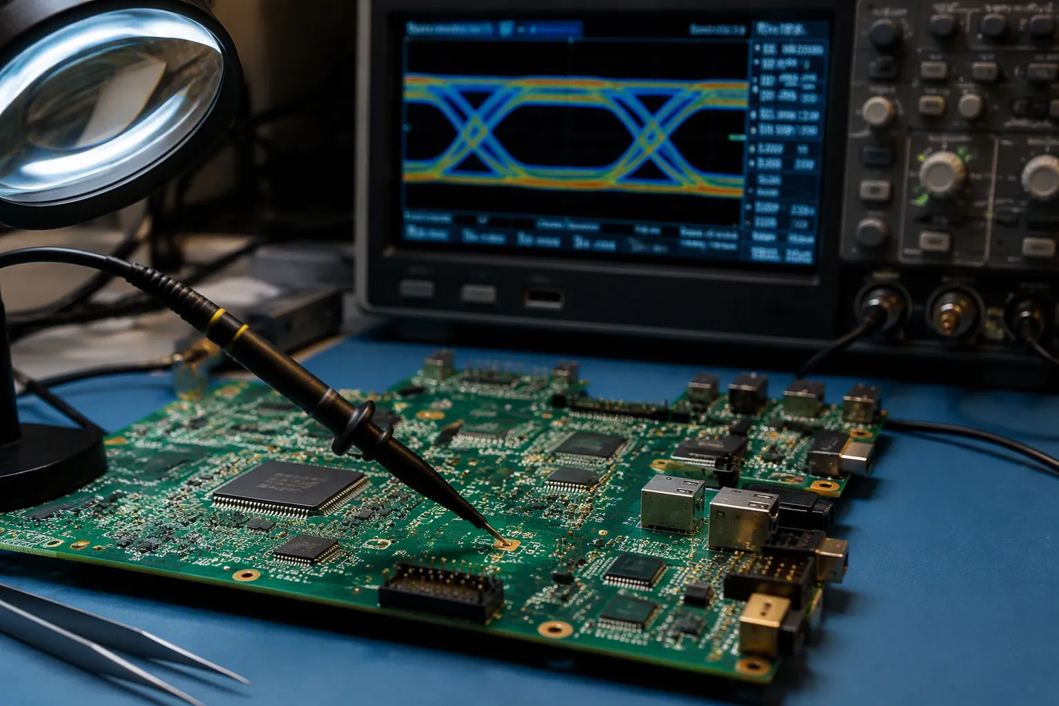
A clock trace runs beside a data line on your board. The clock’s electromagnetic field couples into that data trace and corrupts the signal. Your prototype then fails with data errors that appear and disappear. This is a classic signal integrity problem, and it shows why pcb circuit design must control the physical behavior of the board, not just the logic of the schematic. You may ask: when does a pcb design become a high-speed printed circuit board project, and what should you change first? The answer starts with rise time, not clock frequency. A high-speed pcb demands controlled impedance, solid return paths, and careful routing. Start there.
Key Takeaways
Rise time, not clock frequency, decides if your board is high-speed.
Keep return paths solid to avoid signal errors and EMI.
Choose laminates with low Dk and Df for fast signals.
Match trace lengths and control impedance for clean signals.
Work with your fabricator early to ensure buildable designs.
High-Speed PCB Design Considerations
Rise Time vs. Propagation Delay
You can’t judge a board by its clock frequency alone. A slow clock with a fast edge can still act like a transmission line. The real trigger for high-speed pcb design rules is how signal rise time relates to trace propagation delay. When the rise time is similar to or shorter than the propagation delay, the trace acts as a transmission line. Reflections, crosstalk, and impedance mismatches then become important.
Consider a worked example. A 60 mm trace has a one-way delay of 0.353 ns, while the signal rise time is about 0.25 ns. The trace delay is longer than the edge time. This design sits outside the lumped-element regime, so you need a transmission-line model. A digital signal with a 1 ns rise time on a trace with a 1 ns propagation delay will likely show high-speed characteristics too. At that point, traditional low-frequency rules no longer apply.
In a worked board example, a 60 mm trace has a one-way delay of 0.353 ns while the signal rise time is about 0.25 ns. Because the trace delay is longer than the edge time, the design is outside the lumped-element regime and a transmission-line model is needed.
Critical Length and Board Size
Critical length tells you when a trace becomes electrically long. The critical length lc is the line length over which signal propagation time equals half the fastest rise time. With tr = 1 ns and FR-4 material, the critical length is about 2 inches. Beyond that point, you must design traces as controlled impedance lines. A common industry rule of thumb, the 1/4 rule, states that if trace length exceeds one-fourth of the signal’s electrical rise time, reflections interfere with the signal and impedance matching becomes necessary.
Board size makes this effect stronger. Larger boards and longer traces require high-speed design rules at lower frequencies. A 1 ns rise time on FR-4 gives a critical length difference of about 1 inch under the 1/6 rule. The table below summarizes the key parameters for high-speed pcb design.
Quantity | Condition | Implication |
|---|---|---|
Critical length | lc = tr / (2 * tpd) | One-way propagation time equals half the fastest rise time |
Short line | l < lc / 1.5 | Treat as a lumped element |
Long line | Trace delay comparable to or longer than tr | Model as a transmission line |
For a 1 ns rise time in FR4, a route longer than about 2 inches must be considered a transmission line and is a candidate for controlled impedance routing. This is why high-speed pcb layout demands early attention to board dimensions and net lengths.
Impedance Control and Signal Integrity
Controlled Impedance and Return-Current Paths
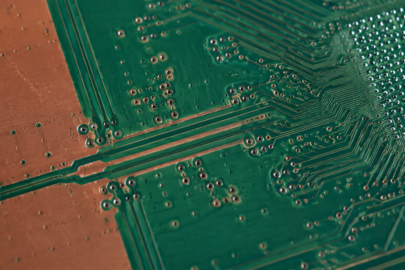
You can’t think about impedance control without the return path. A trace sends signal current forward, and nearby ground planes send it back. At high frequencies, return current takes the path with the least inductance. That means it flows right under the signal trace. This close coupling keeps the loop area small and keeps the characteristic impedance steady.
Any break in that path ruins everything. A slot, cutout, or clearance hole makes the return current take a detour. Loop inductance goes up, and the trace acts like an antenna. Place stitching vias close to any signal via that changes reference planes.
Controlled impedance matters because PCB traces act like transmission lines. Any mismatch along the path causes signal reflection, waveform distortion, and data corruption. Even a trace narrowed over a short BGA breakout region creates reflections and a small phase shift at high frequencies.
To get a reflection-free signal, high-speed nets need impedance matching. This means the driver, the transmission line, and the receiver must show as little impedance difference as possible. Unmatched signals show major distortion.
Common targets guide your stackup. DDR4/DDR5 single-ended signals target 40–50 Ω and need careful length matching, crosstalk control, and tight timing margins. Differential interfaces must meet the specified differential impedance target for each protocol. Use the manufacturer’s impedance tables for trace width and spacing instead of generic field-solver guesses.
Ground Planes, Plane Edges, and EMI
A solid ground plane lowers inductance and helps both analog and digital performance. It gives every high-speed signal a low-impedance return path and keeps the power delivery network stable. Poor power integrity causes voltage droop and jitter. That then makes circuit board signal integrity worse.
Splits in the ground plane break this stability. They force return current to detour, couple noise between sections, and create impedance mismatches for any signal crossing the gap. A split ground plane can act like a slot antenna and radiate EMI. Keep high-speed signals over a solid ground plane and don’t route across splits. If a split crossing can’t be avoided, route the trace perpendicular to the split and place a stitching capacitor close to the crossing.
Board edges cause a similar problem. Keep high-speed traces away from board or plane edges. This stops impedance variation and EMI leakage at the edges. Stitch vias around ground-plane edges to form a shielding cage that cuts radiated EMI.
These rules tie right into your bigger goals. When you design a high-speed pcb, impedance control, continuous return paths, and a stable power delivery network work together. Each one helps signal integrity performance. Get them right, and your controlled-impedance lines act predictably from driver to receiver.
Material Selection for High-Speed PCB Design
Key Laminate Properties: Dk and Df
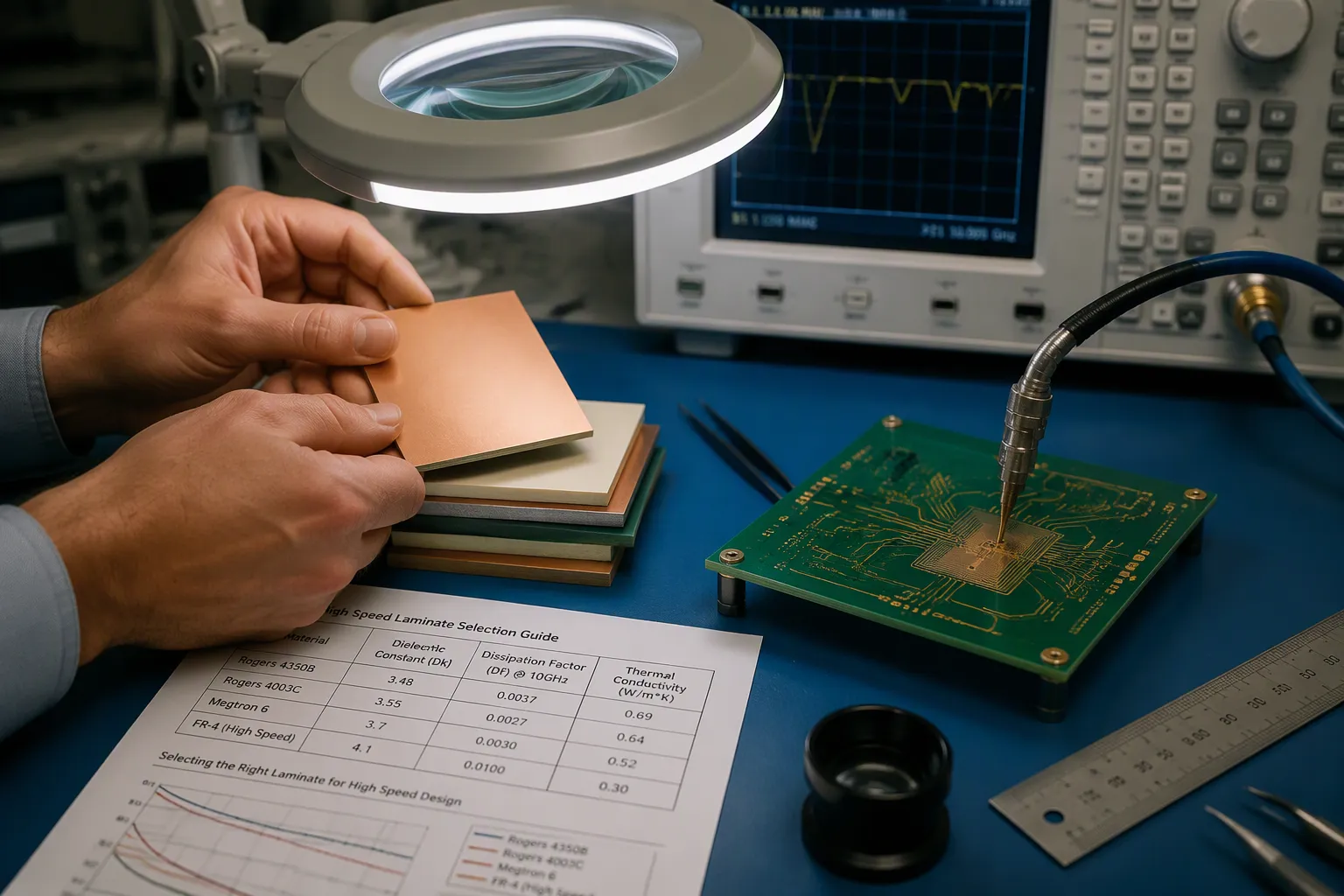
The laminate you choose decides the basic electrical behavior of the whole board. Two properties matter most: dielectric constant (Dk) and dissipation factor (Df). Dk controls how fast signals travel and affects characteristic impedance. Df tells how much signal energy the dielectric turns into heat. A low Dk lets signals travel faster and cuts crosstalk between traces. A low Df helps more signal energy reach the receiver.
Standard FR-4 has a Dk around 4. High-speed laminates use lower-Dk, lower-Df materials to reduce dielectric loss. For high-frequency designs, keep Df as low as practical at your operating frequency. PTFE-based laminates, spread glass laminates, and high-Tg materials such as 370HR, Megtron, or Duroid are common low-loss choices. The chart below compares Dk and Df across common laminates.
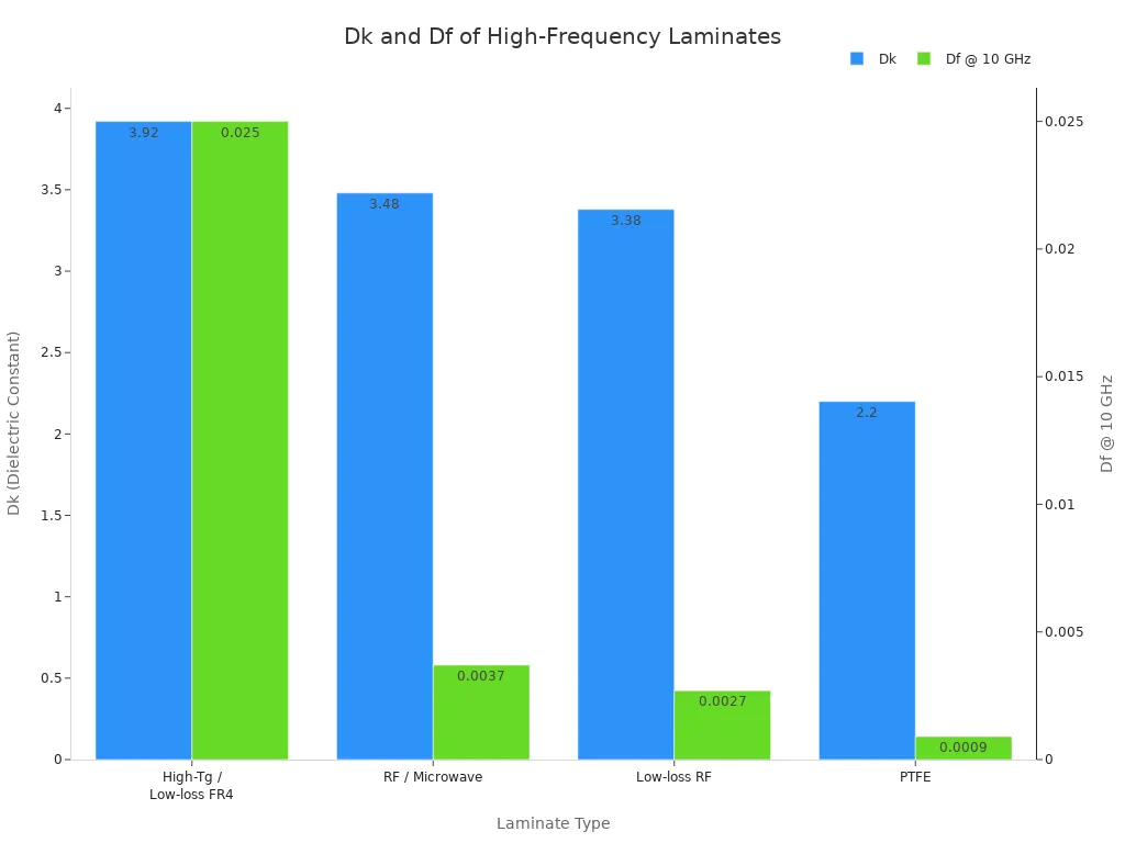
Propagation delay goes up with the square root of effective Dk. A higher Dk makes signals slower and shortens the wavelength on the board. That shift changes impedance and requires tighter trace spacing. For matched-delay interfaces like DDR memory, Dk changes with frequency or temperature and can cause timing skew. Pick laminates with stable Dk and a good Dk-versus-frequency curve.
Laminate Type | Example | Dk | Df (@10 GHz) | Tg | Best Use |
|---|---|---|---|---|---|
Standard FR4 | Generic FR4 | ≈4 | — | — | Digital, power, shorter high-speed routes |
Low-loss high-speed | PTFE-based, spread glass, or high-Tg (e.g., 370HR, Megtron, Duroid) | — | — | — | Longer high-speed channels |
Spread glass | Spread glass laminates | — | — | — | Longer high-speed channels |
PTFE | PTFE-based laminates | — | — | — | Longer high-speed channels |
High-Tg laminates resist softening during lead-free reflow. They also limit Z-axis expansion so plated through-holes do not crack. Low moisture absorption and high chemical resistance also matter for harsh environments.
Copper Roughness, Cost, and Availability
Copper surface roughness is a real loss factor at high frequencies. The skin effect pushes current to the conductor surface. A rough surface forces current to climb peaks and valleys, so the electrical path becomes longer and resistance rises. This roughness increases insertion loss and causes local impedance changes, which lead to reflections and timing instability.
Managing copper roughness is part of low-loss design, and cost and availability affect these choices. PTFE-based laminates and other low-loss materials cost more and need special processing. FR4-grade laminates may suffice for shorter routes, while longer high-speed channels may require low-loss materials. Check which materials your fabricator stocks early. A laminate that fits your layer stack-up but has a long lead time will stall your schedule. Build your impedance control targets around materials your fabricator already carries.
Routing Techniques for High-Speed Signal Integrity
Good routing starts before you draw anything. Run simulations early to find signal problems before making the board. Pre-layout simulation checks trace widths, stack-up choices, and impedance targets. Post-layout simulation finds layout issues like parasitic effects and reflections. Skipping either step leads to costly fixes.
Verification Stage | When to Run It | What to Check |
|---|---|---|
Pre-layout | Before the layout is final | Trace widths, stack-up, impedance targets, crosstalk |
Post-layout | After the layout is final | Parasitics, impedance mismatches, reflections |
Differential Pair Routing and Skew Management
Differential signaling suits fast, critical signals. Its return path loops inside the pair, so opposite signals cancel. This boosts immunity to noise and lowers EMI. Keep both lines equal in length, keep width and spacing constant, and minimize impedance changes along the run.
Skew control matters most in parallel interfaces. Match trace lengths to fix timing skew between data signals, data and strobe, and clock and address. Use differential pair routing controls to minimize skew and meet the differential impedance target. Validate critical channels with extracted S-parameters and eye diagram analysis before fabrication.
Spacing drives crosstalk. Widening pair-to-pair spacing and keeping clearances consistent reduce crosstalk. Set your differential impedance targets from the stack-up, then let spacing and trace width follow.
Via Optimization and Length Matching
Vias hurt fast signals. A via stub acts like an open-ended transmission line and creates a sharp notch in insertion loss. Backdrilling eliminates or shortens stubs and improves return loss and jitter.
Faster signals need tighter length matching. For DDR4/DDR5, match data lines within each byte lane, and keep data-to-strobe and clock skew inside the controller vendor’s timing budget. A common mistake is over-matching DQ and under-matching the clock, which times everything else on the bus.
Keep your practical priorities in order for high-speed pcb layout: solid reference planes, no edge routing, shorter vias, matched lengths, and controlled spacing. These choices matter more than any single tool setting.
Aligning PCB Circuit Design with Fab Capabilities
Early DFM Collaboration and Impedance Tolerances
Your design only works if the fabricator can really build it. Bring the fab house into the talk before you lock in the layer stack-up. Early reviews catch problems that cost real money later. Common DFM gaps include old layout habits, outdated rule libraries, late fabricator involvement, and no clear DFM owner. Fix these with shared rule libraries, standard output formats, and one named person who signs off on DFM.
Fabricator limits shape your impedance targets. Minimum trace width, etch precision, plating, lamination, and registration all shift the finished geometry away from your drawn data, and that variation moves impedance in a high-speed pcb. Stick to a standard impedance tolerance unless tighter control truly matters. Tighter specs raise cost and scrap rates. Specify impedance targets, not dielectric thicknesses, so the fabricator can tune the recipe. Confirm material availability and standard stock thicknesses early, because low-loss laminates often carry long lead times.
Prototypes, Coupons, and Simulation Validation
You cannot trust a prototype you never measured. Impedance coupons sit on the same production panel as your board. They share the same stackup, materials, copper thickness, and process conditions. Coupons mirror your critical structures, such as single-ended traces and differential pairs. Time Domain Reflectometry (TDR) sends a fast voltage step into the coupon and records reflections. A flat trace means constant impedance near target. Bumps or dips point to etching or lamination variation.
Run signal-integrity simulations first. TDR works best after simulation flags a mismatch or after prototype measurements show ringing or eye closure. Compare the measured impedance profile against your simulated targets. Combine TDR time-domain data with frequency-domain S-parameter measurements to locate the exact discontinuity. Correlate the waveform signature with layout features like vias, stubs, and neck-downs. Then adjust the design and re-measure. This loop gives you objective proof that your high-speed pcbs meet the agreed impedance window before production.
You now know the main choices to make. First, find your high-speed nets. Next, set your impedance control targets. Pick materials that help signal integrity. Use routing rules for pairs, vias, and lengths. Then talk with your fabricator early.
Good pcb design controls physical things. Simulation by itself cannot fix a weak stackup. Your high-speed pcb design works when the board itself acts well. Treat every pcb design choice as a physical one.
Write down your needs. Go over stackup and materials with your fabricator. Check prototypes before production.
FAQ
When should I treat my board as a high-speed design?
Compare rise time against trace propagation delay, not clock frequency. Even a slow clock with a fast edge can act as a transmission line. In FR-4, a 1 ns rise time means any route over about 2 inches needs transmission-line modeling. Bigger boards hit this limit at lower frequencies.
What impedance targets should I set for common interfaces?
DDR4/DDR5 single-ended signals target 40–50 Ω and need careful length matching, crosstalk control, and tight timing margins. Differential interfaces must meet the specified differential impedance target for each protocol. Get trace width and spacing from your fabricator’s impedance tables, not generic field-solver guesses.
Do I really need low-loss laminate for my design?
Only if your signals are fast enough to lose energy in the dielectric. FR4-grade laminates may suffice for shorter routes, but longer high-speed channels may require low-loss materials. Low-Dk, low-Df laminates reduce dielectric loss, but they cost more and have longer lead times. Check stock early.
How tight should my impedance tolerance be?
Stick to a standard impedance tolerance unless tighter control truly matters. Tighter specs increase cost and scrap rates. Set impedance targets, not dielectric thicknesses, so your fabricator can adjust the recipe. Check material availability and standard stock thicknesses before you lock the stack-up.
What should I validate before production?
Run pre-layout and post-layout simulations first. Next, measure impedance coupons on the same production panel with TDR. Compare the measured profile with your simulated targets. Match waveform bumps to layout features like vias and neck-downs. Modify, re-measure, and only then release the pcb design to production.