How to assemble the finished PCB product step by step?
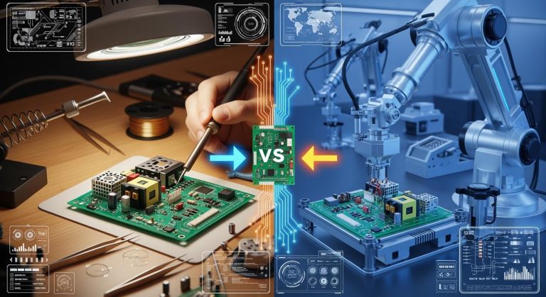
Printed Circuit Board (PCB) assembly transforms bare boards into functional electronic devices. It involves placing components like resistors, capacitors, and microchips onto the PCB and securing them with solder. This process forms the backbone of modern electronics manufacturing, supporting industries like telecommunications, automotive, and consumer electronics.
You can see its significance in the global market. Asia-Pacific leads PCB production, driven by investments in 5G infrastructure. China alone plans to deploy millions of 5G base stations, creating high demand for local PCBs. South Korea and Japan require advanced PCBs for smart factories and autonomous vehicles. Europe and North America are also increasing investments, boosting PCB manufacturing for telecom upgrades.
Mastering the PCB assembly process equips you with essential skills for a thriving career in electronics. It opens doors to roles in design, manufacturing, and quality control, making you a valuable asset in this rapidly growing field.
Key Takeaways
- Learn how to put together PCBs to improve your skills and job chances in electronics.
- Use a step-by-step process like getting materials ready, adding solder paste, and testing to make sure it works well.
- Use important tools like soldering irons and multimeters to build and test PCBs.
- Stay safe by wearing protective gear and keeping your workspace clean and tidy.
- Keep learning about new trends and technologies to stay ahead in the PCB industry.
Overview of the PCB Assembly Process
Key stages in PCB assembly
The PCB assembly process involves several critical steps that transform a bare board into a functional electronic device. Each stage demands careful execution to ensure the final product meets industry standards.
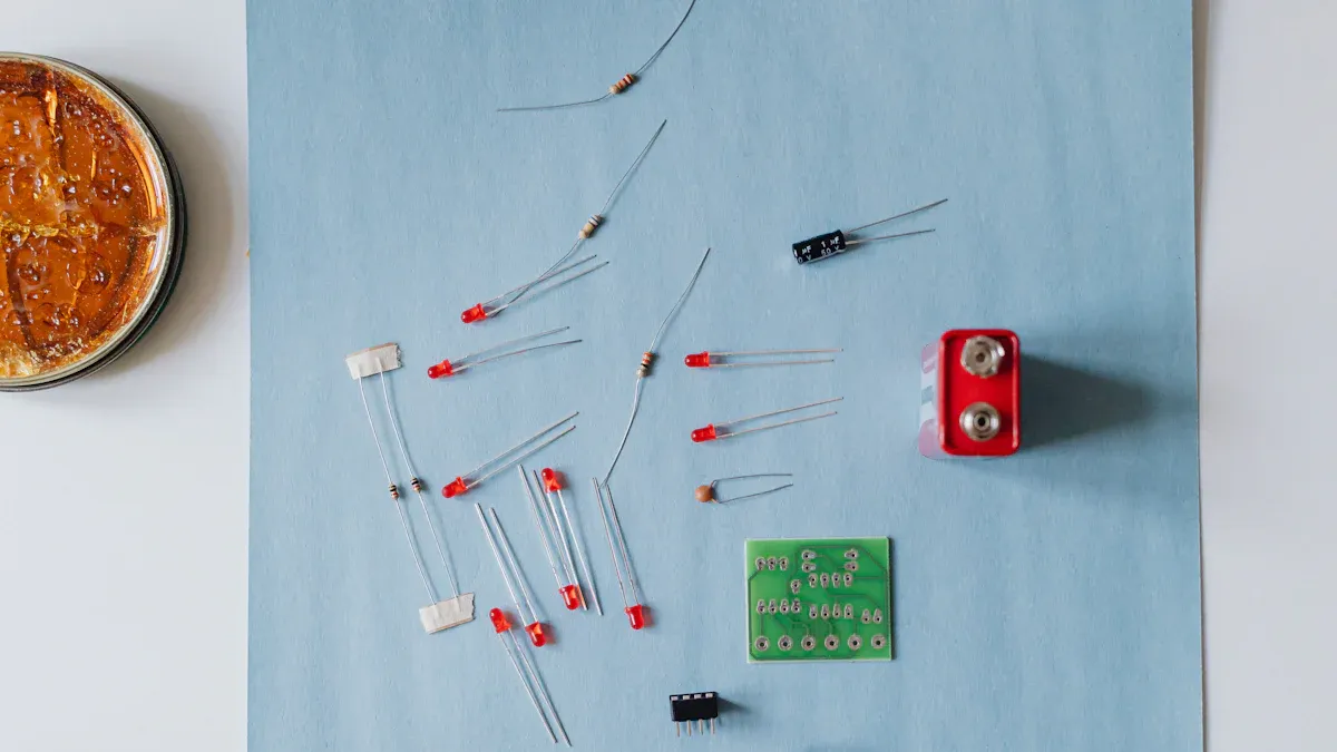
- Material Preparation and Pre-Assembly Inspection: You begin by gathering all necessary components and inspecting the PCB for defects. This step ensures the board and parts are ready for assembly.
- Solder Paste Application: A stencil is used to apply solder paste to specific areas of the PCB where components will be placed.
- Automated Surface-Mount Technology (SMT) Placement: Machines precisely place surface-mount components onto the board.
- Reflow Soldering: The board passes through a reflow oven, melting the solder paste and securing the components.
- Automated Optical Inspection (AOI): You use specialized equipment to check for soldering defects and misplaced components.
- Selective Wave Soldering: For through-hole components, this step involves soldering them using a wave of molten solder.
- Manual Inspection and Rework: You manually inspect the board and fix any issues that automated processes missed.
- Functional Testing: The assembled PCB undergoes tests to verify its performance and functionality.
- Conformal Coating or Potting: Protective coatings are applied to shield the PCB from environmental factors.
- Final Assembly and Packaging: The completed PCB is packaged for shipment or integration into larger systems.
By following these stages, you ensure the PCB assembly process is efficient and reliable.
Importance of precision and quality control
Precision and quality control are the cornerstones of successful PCB assembly. Even minor errors can lead to malfunctioning devices or costly rework. To maintain high standards, you must monitor key metrics throughout the process.
| Metric Type | Description |
|---|---|
| Overall pass/fail rate | Indicates the success rate of the assembly process. |
| Average values for key parameters | Provides insights into the typical performance of solder paste application. |
| Standard deviations | Assesses the consistency of the process, highlighting variability. |
| Detailed Pad-level Data | Individual measurements for each pad help identify specific issues. |
| Trend Analysis | Charts that show variations help in monitoring process stability. |
| Defect Maps | Visuals that categorize defects assist in targeted improvements. |
| Statistical Process Control (SPC) | Control charts help in identifying shifts in the process. |
| Root Cause Analysis | Deep data analysis to find underlying issues when defects occur. |
You can use tools like real-time monitoring and predictive maintenance to catch issues early and optimize the process. Machine learning algorithms also enhance defect prediction, ensuring consistent quality. By prioritizing precision and quality control, you build reliable PCBs that meet industry demands.
Tools and Equipment for PCB Assembly
Basic tools for beginners
Starting with PCB assembly requires a few essential tools. These tools help you handle components and solder them onto the board effectively.
- Soldering Iron: A basic soldering iron allows you to melt solder and secure components. Choose one with adjustable temperature settings for better control.
- Solder Wire: Use lead-free solder wire for environmental safety. Thin solder wires work best for small components.
- Tweezers: Precision tweezers help you pick and place tiny components accurately.
- Magnifying Glass: A magnifying glass or loupe lets you inspect solder joints and small parts closely.
- PCB Holder: A holder stabilizes the board during assembly, preventing accidental movement.
- Multimeter: This tool checks electrical connections and verifies circuit functionality.
These tools form the foundation of your PCB assembly process. They are affordable and easy to use, making them ideal for beginners.
Advanced equipment for professional assembly
Professional PCB assembly demands advanced equipment to ensure precision and efficiency. These tools handle complex tasks and meet industry standards.
- In-Circuit Testing (ICT): This equipment checks the electrical performance of individual components on the PCB.
- Functional Testing (FCT): FCT verifies the overall functionality of the assembled PCB.
- Reflow Oven: A reflow oven with 10-zone temperature control ensures uniform soldering for surface-mount components.
- Wave Soldering Machine: This machine handles through-hole components with molten solder waves.
- Automated Optical Inspection (AOI): AOI systems detect soldering defects and misaligned components.
- Pick-and-Place Machine: These machines achieve placement accuracy of ±0.025mm, ideal for high-density boards.
| Specification | Details |
|---|---|
| Placement Accuracy | ±0.025mm |
| Reflow Soldering | 10-zone temperature control |
| Board Size | 10mm × 10mm to 450mm × 450mm |
| Layer Count | 1-40 layers |
| Minimum Trace/Space | 3/3mil |
| Surface Finish | HASL, ENIG, OSP, Immersion Silver, Immersion Tin |
| Package Types | SMD, Through-hole, BGA, QFP, QFN, SOP, PLCC |
These tools and specifications reflect the growing demand for high-quality PCB assembly in industries like automotive and medical devices.
Safety gear and precautions
Safety is crucial during PCB assembly. You must protect yourself and the components from harm.
- Anti-Static Wrist Strap: This strap prevents electrostatic discharge, which can damage sensitive components.
- Safety Glasses: Wear safety glasses to shield your eyes from solder splashes.
- Ventilation System: Ensure proper ventilation to avoid inhaling fumes from soldering.
- Heat-Resistant Gloves: Use gloves to protect your hands from burns while handling hot tools.
- Fire Extinguisher: Keep a fire extinguisher nearby to address any accidental fires.
Tip: Always work in a well-lit area and follow manufacturer guidelines for tool usage. Proper safety measures ensure a smooth and hazard-free PCB assembly process.
Step-by-Step Guide to Assembling a Finished PCB Product
Preparing the workspace
A well-organized workspace is the foundation of a successful PCB assembly process. You need to ensure that your workspace is clean, well-lit, and free from dust or debris. Dust particles can interfere with soldering and cause defects in the final product. Arrange your tools and components within easy reach to avoid unnecessary movement during assembly.
Tip: Use an anti-static mat on your workbench to prevent electrostatic discharge (ESD), which can damage sensitive electronic components.
Keep your workspace ventilated to minimize exposure to soldering fumes. A fume extractor or a small fan can help maintain air quality. Label your components and tools to avoid confusion, especially when working with multiple parts.
Failing to prepare your workspace properly can lead to misplaced components, poor soldering, or even damage to the PCB. By taking the time to set up your workspace, you create an environment that supports precision and efficiency.
Inspecting the PCB and components
Before starting the assembly, inspect the PCB and components thoroughly. This step ensures that all parts are in good condition and meet quality standards. Begin by examining the PCB surface for cleanliness and defects. Any dirt, grease, or residue can affect solder adhesion. Clean the PCB with isopropyl alcohol if necessary.
Check the components for physical damage, such as bent leads or cracks. Use a magnifying glass or a microscope to inspect small parts. Rigorous pre-treatment of PCB surfaces ensures proper adhesion and reduces the risk of defects.
Here are some key inspection guidelines:
- Use UV light to check the coating coverage and uniformity on the PCB.
- Perform Automated Optical Inspection (AOI) to detect misalignments or insufficient solder.
- Conduct In-Circuit Testing (ICT) to verify the electrical performance of individual components.
- AOI uses high-definition cameras to scan the PCB for defects.
- It flags issues like misaligned components or insufficient solder for review.
- This process ensures that only high-quality boards proceed to the next stage.
PCB testing is critical for industries like automotive and aerospace, where reliability is essential. Skipping this step can result in malfunctioning devices or costly rework. By inspecting the PCB and components, you ensure a smooth assembly process and a reliable final product.
Applying solder paste
Solder paste application is a crucial step in the PCB assembly process. The paste acts as an adhesive, holding components in place before soldering. It also provides the necessary material for creating strong electrical connections.
To apply solder paste, use a stencil that matches the PCB layout. Align the stencil carefully over the board to ensure the paste is applied only to the designated areas. Use a squeegee to spread the paste evenly across the stencil. Apply consistent pressure to avoid uneven distribution.
Note: Uneven solder paste application can lead to weak solder joints or short circuits.
After applying the paste, inspect the board to ensure that the paste covers all the required pads. Remove any excess paste to prevent bridging between components.
Incorrect solder paste application can cause several issues, such as:
- Bridging: Excess paste creates unintended connections between pads.
- Insufficient solder: Too little paste results in weak joints.
- Misalignment: Misplaced paste can prevent components from sitting correctly.
By applying solder paste with precision, you set the stage for a successful soldering process. This step directly impacts the quality and functionality of the final PCB product.
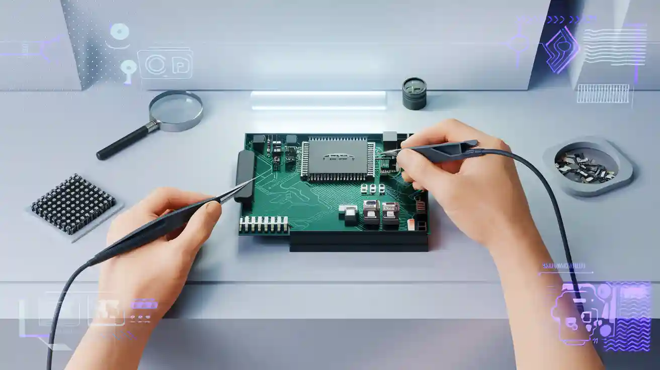
Placing components on the PCB
Placing components on the PCB is a critical step in the PCB assembly process. It requires precision and attention to detail to ensure proper alignment and functionality. You must carefully position each component on the board according to the design layout.
Start by referring to the PCB’s assembly drawing or bill of materials (BOM). These documents guide you in identifying the correct placement for each component. Use tweezers to handle small parts like resistors, capacitors, and diodes. For surface-mount components, ensure the solder paste applied earlier aligns with the component pads.
Tip: Double-check the polarity of components like diodes and electrolytic capacitors. Incorrect placement can cause the circuit to malfunction.
Automated pick-and-place machines are often used in professional settings. These machines achieve high accuracy and speed, placing thousands of components per hour. However, for manual assembly, you must rely on steady hands and a magnifying glass to ensure proper alignment.
Incorrect placement can lead to several issues:
- Misaligned components: This can cause poor electrical connections or short circuits.
- Reversed polarity: Components like LEDs and capacitors may fail if installed backward.
- Overlapping parts: Crowded placements can interfere with soldering and testing.
By taking your time and following the layout carefully, you can avoid these problems and ensure a smooth assembly process.
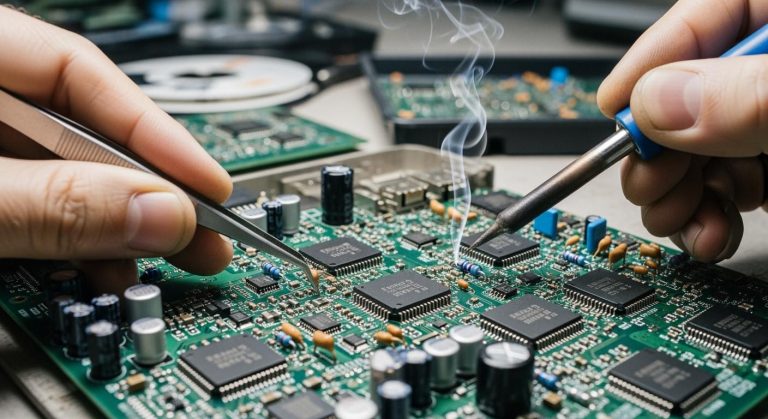
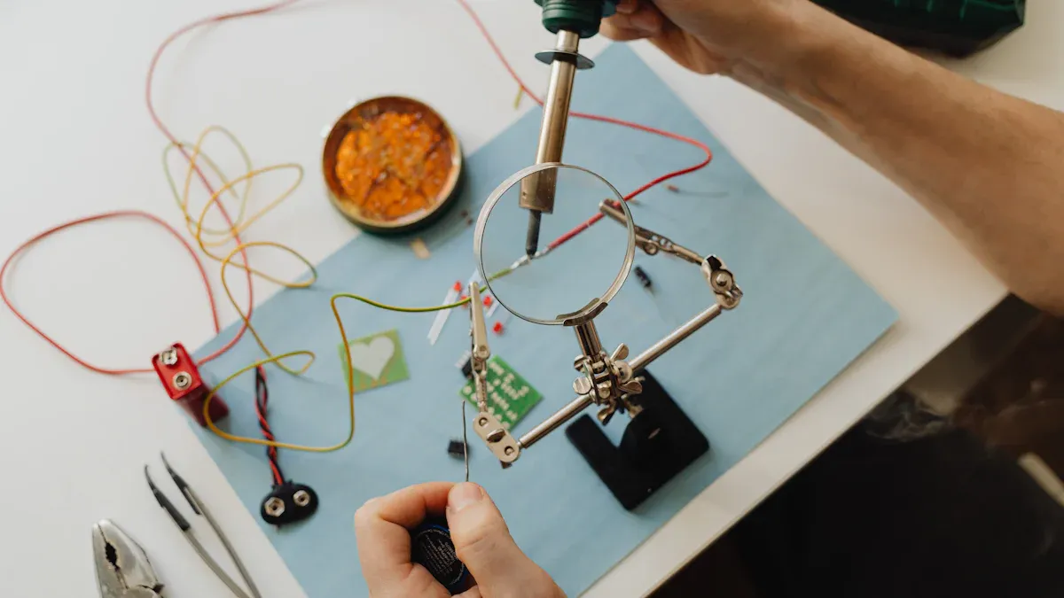
Soldering the components
Soldering secures the components to the PCB and establishes electrical connections. This step demands precision and adherence to industry standards to ensure reliability.
For surface-mount components, reflow soldering is the most common method. The PCB, with components placed on it, passes through a reflow oven. The oven heats the solder paste, causing it to melt and bond the components to the board. Ensure the oven’s temperature profile matches the solder paste’s specifications.
Through-hole components require manual or wave soldering. In manual soldering, use a soldering iron to heat the component lead and pad simultaneously. Apply solder wire to create a strong joint. Wave soldering involves passing the PCB over a wave of molten solder, which bonds the leads to the board.
Note: Always use solder flux to improve the flow of solder and prevent oxidation.
Common soldering defects include:
- Cold solder joints: These occur when the solder fails to bond properly, leading to weak connections.
- Bridging: Excess solder creates unintended connections between adjacent pads.
- Insufficient solder: This results in poor electrical conductivity and unreliable joints.
To minimize defects, follow the IPC J-STD-004B standard for soldering fluxes. Research also highlights the importance of mapping soldering heat requirements, especially in selective wave soldering. Proper soldering techniques ensure the PCB assembly process produces reliable and durable products.
Cleaning the PCB
Cleaning the PCB removes residues left behind during soldering, such as flux and solder splashes. These residues can cause corrosion or electrical leakage if not removed.
Use isopropyl alcohol (IPA) and a lint-free cloth to clean the board. Gently scrub the surface to remove flux residues. For hard-to-reach areas, use a soft brush or an ultrasonic cleaner. Ensure the board is completely dry before proceeding to the next step.
Tip: Use a UV light to inspect the board for any remaining residues.
Neglecting this step can lead to several issues:
- Corrosion: Residual flux can corrode the PCB over time, reducing its lifespan.
- Electrical leakage: Contaminants can create unintended conductive paths, causing malfunctions.
- Poor adhesion: Residues can interfere with protective coatings applied later.
By thoroughly cleaning the PCB, you enhance its reliability and prepare it for final testing and packaging.
Testing and troubleshooting
Testing and troubleshooting ensure the PCB functions as intended and meets quality standards. This step identifies and resolves issues before the final product is delivered.
Start by performing functional testing. Use a multimeter or specialized testing equipment to verify electrical connections and circuit functionality. Check for continuity between pads and components. If a connection fails, inspect the solder joints for defects like cold solder or bridging.
For advanced testing, employ tools like Automated Optical Inspection (AOI) and X-ray inspection. AOI scans the PCB for surface defects, such as misaligned components or insufficient solder. X-ray inspection reveals hidden issues, like voids in solder joints or internal fractures in components.
Tip: Use thermal imaging to detect overheating components. Excess heat often indicates a short circuit or incorrect placement.
Troubleshooting involves identifying the root cause of any issues. Begin by isolating the faulty section of the PCB. Use a systematic approach to test each component individually. Replace damaged parts and re-solder weak joints.
Common problems during testing include:
- Open circuits: Missing or broken connections prevent current flow.
- Short circuits: Unintended connections between pads cause excessive current.
- Component failure: Damaged parts, like capacitors or ICs, disrupt functionality.
By addressing these issues, you ensure the PCB assembly process produces reliable and high-performing products. Testing and troubleshooting are critical for industries like telecommunications and medical devices, where precision is non-negotiable.
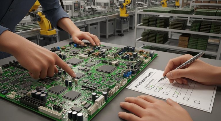
Final inspection and packaging
Final inspection and packaging confirm the PCB meets quality benchmarks and is ready for delivery. This step safeguards the product’s reliability and ensures customer satisfaction.
Begin with a visual inspection. Examine the PCB for surface defects, such as scratches, solder splashes, or misaligned components. Use magnifying tools or UV light to enhance visibility.
Advanced testing protocols validate the PCB’s performance. These include:
- X-ray inspection: Detects internal defects, like voids or fractures.
- Automated Optical Inspection (AOI): Identifies soldering issues and component misplacement.
- Electrical testing: Verifies circuit functionality and checks for shorts or opens.
Post-soldering testing ensures solder joint quality. Use thermal imaging to detect heat-related issues and cross-sectional analysis to examine joint integrity.
Callout: Packaging plays a vital role in protecting the PCB during transit.
Follow these quality benchmarks for inspection:
- Solderability Testing: Ensure solder adheres properly to pads and leads.
- Peel Strength Testing: Measure the copper layer’s adhesion strength to the board.
- Contamination Testing: Check for residues that could cause corrosion or shorts.
Once the PCB passes inspection, package it securely. Use anti-static bags to prevent electrostatic discharge. Add cushioning materials to protect the board from physical damage. Label the package with relevant details, such as product specifications and handling instructions.
Incorrect packaging can lead to damaged PCBs during transit. By prioritizing inspection and packaging, you deliver a product that meets industry standards and customer expectations.
Common Challenges in the PCB Assembly Process
Handling small components
Managing small components during PCB assembly can be tricky. These parts, such as microchips and resistors, require precise handling to avoid damage or misplacement. You need steady hands and the right tools, like precision tweezers and magnifying glasses, to position them accurately.
Small components often follow strict standards to ensure quality. For example, IPC-A-610 defines acceptable solder joint criteria, while ISO 13485 ensures compliance for medical devices. These certifications guide you in maintaining high-quality assembly practices.
| Certification/Standard | Relevance to SMT |
|---|---|
| IPC-A-610 | Acceptable solder joint standards (Class 1: General electronics; Class 3: Aerospace/medical) |
| IATF 16949 | Automotive-specific quality management (mandatory for automotive SMT suppliers) |
| ISO 13485 | Medical device manufacturing compliance |
| RoHS/REACH | Compliance with hazardous substance restrictions |
When handling micro-components, you must also minimize defects like solder joint opens or misaligned parts. Industries like automotive and medical devices demand extremely low defect rates, as shown below:
| Defect Type | Consumer Electronics | Automotive | Medical Devices |
|---|---|---|---|
| Solder Joint Opens | <50 ppm | <10 ppm | <5 ppm |
| Misaligned Components | <30 ppm | <5 ppm | <2 ppm |
| Cold Solder | <20 ppm | <3 ppm | <1 ppm |
By following these standards and using proper tools, you can handle small components effectively and reduce errors.
Avoiding soldering defects
Soldering defects can compromise the functionality of your PCB. Common issues include cold solder joints, bridging, and insufficient solder. These defects often result from improper soldering techniques or inadequate heat application.
To avoid these problems, you must follow industry standards like IPC-A-610, which outlines acceptable solder joint criteria. Use solder flux to improve adhesion and prevent oxidation. Ensure your soldering iron is set to the correct temperature to create strong, reliable joints.
Cold solder joints occur when the solder fails to bond properly. You can prevent this by heating both the pad and the component lead evenly. Bridging happens when excess solder creates unintended connections between pads. To fix this, apply solder sparingly and use a desoldering tool to remove excess material.
Tip: Regularly inspect solder joints under magnification to catch defects early.
By mastering soldering techniques and adhering to standards, you can minimize defects and ensure your PCB performs reliably.
Ensuring proper alignment and placement
Proper alignment and placement of components are essential for a functional PCB. Misaligned parts can cause electrical failures or short circuits, leading to costly rework. You must carefully follow the assembly drawing or bill of materials (BOM) to position each component accurately.
For surface-mount components, automated pick-and-place machines offer high precision. These machines achieve placement accuracy of ±0.025mm, making them ideal for high-density boards. However, manual assembly requires steady hands and tools like tweezers and magnifying glasses.
Misalignment often results from rushing the placement process or neglecting polarity checks. Components like diodes and capacitors must be oriented correctly to function. Double-check the polarity before soldering to avoid errors.
Callout: Misaligned components can lead to defects like open circuits or overheating.
By taking your time and using the right tools, you can ensure proper alignment and placement, reducing the risk of defects and improving the overall quality of your PCB.
Starting a Career in PCB Assembly and Manufacturing
Skills required for PCB assembly
To excel in PCB assembly, you need a mix of technical and practical skills. Precision is key when handling small components and soldering them onto the board. You must develop steady hands and sharp attention to detail to avoid errors like misaligned parts or soldering defects. Familiarity with tools such as soldering irons, tweezers, and multimeters is essential.
Understanding circuit diagrams and schematics helps you identify component placement and troubleshoot issues. Basic knowledge of electronics, including concepts like voltage, current, and resistance, strengthens your ability to test and repair circuits. You also need problem-solving skills to address challenges like short circuits or component failures.
Soft skills like time management and teamwork are equally important. Many PCB assembly roles involve working in teams to meet production deadlines. By mastering these skills, you prepare yourself for a successful career in this field.
Educational pathways and certifications
You can start your journey in PCB assembly by pursuing relevant educational programs. Vocational schools and community colleges often offer courses in electronics and PCB manufacturing. These programs teach you the fundamentals of circuit design, soldering techniques, and quality control.
Certifications enhance your credibility and open doors to better opportunities. The IPC-A-610 certification, for example, validates your knowledge of soldering standards. If you aim to work in specialized industries like automotive or medical devices, certifications like IATF 16949 or ISO 13485 are valuable.
Online platforms also provide affordable courses on PCB assembly. Websites like Coursera and Udemy offer beginner-friendly modules that cover essential topics. By investing in education and certifications, you build a strong foundation for your career.
Entry-level roles in the industry
The PCB assembly industry offers various entry-level roles to help you gain hands-on experience. As a PCB assembler, you’ll work on tasks like soldering components, testing circuits, and inspecting boards for defects. This role introduces you to the practical aspects of manufacturing.
If you prefer working with machines, consider becoming an SMT operator. In this role, you’ll operate pick-and-place machines and reflow ovens to assemble high-density boards. Quality control technician roles focus on inspecting finished PCBs and ensuring they meet industry standards.
The growing demand for skilled professionals makes these roles highly accessible. The PCB market is projected to grow from USD 80 billion in 2024 to USD 120 billion by 2033, with a CAGR of 5.5%. Industries like consumer electronics, automotive, and telecommunications are driving this growth.
- Rising demand for smartphones, tablets, and wearables.
- Expansion of electric vehicles and advanced driver-assistance systems.
- Rollout of 5G technology and IoT applications.
By starting in these entry-level positions, you gain valuable experience and set yourself up for career advancement in PCB assembly and manufacturing.
Tips for gaining hands-on experience
Hands-on experience is essential for mastering PCB assembly. It helps you develop practical skills and build confidence in handling tools and components. Here are some effective ways to gain experience:
- Participate in DIY Electronics Projects
Start with simple projects like assembling LED circuits or building a basic amplifier. These projects introduce you to soldering, component placement, and circuit testing. Websites like Instructables and YouTube offer step-by-step tutorials for beginners.Tip: Keep a project journal to document your progress and troubleshoot issues.
- Join Maker Communities and Workshops
Maker spaces and electronics clubs provide access to tools, equipment, and mentorship. You can collaborate with others on projects and learn advanced techniques. Many communities host workshops on PCB design and assembly.Callout: Networking with experienced makers can open doors to internships and job opportunities.
- Volunteer for Electronics Repair Services
Offer to repair devices like smartphones or laptops for friends and family. This exposes you to real-world challenges, such as diagnosing faults and replacing damaged components. - Enroll in Practical Training Programs
Look for vocational schools or online courses that include hands-on labs. Programs with live demonstrations and practice sessions help you refine your skills.
| Platform | Features |
|---|---|
| Coursera | Beginner-friendly PCB courses |
| Udemy | Affordable hands-on tutorials |
| Local Maker Labs | Access to tools and mentorship |
- Experiment with Open-Source PCB Designs
Download open-source PCB layouts and assemble them yourself. This teaches you how to interpret schematics and follow design guidelines.Emoji Tip: 🛠️ Practice regularly to improve your precision and speed.
By actively engaging in these activities, you build the expertise needed for a successful career in PCB assembly.
Industry Insights and Future Trends in PCB Manufacturing
The growing demand for PCBs in various industries
The demand for PCBs continues to rise across multiple industries due to advancements in technology and increasing reliance on electronic systems. You can see significant growth in sectors like communication networks and automotive electronics.
| Segment | Key Insights |
|---|---|
| Communication Network Infrastructure | Transitioning from 4G to 5G drives higher PCB demand for network equipment. |
| Automotive Electronics | Vehicle electrification and automation increase PCB requirements in modern vehicles. |
Modern vehicles now integrate complex electronic systems for electrification and automation. Advanced driver assistance systems (ADAS) and infotainment systems rely heavily on sophisticated PCBs.
| Driver | Impact on PCB Demand |
|---|---|
| Electrification | Increased complexity in electronic systems leads to higher PCB integration in vehicles. |
| Automation | Electric and autonomous vehicles require advanced PCBs for managing electrical and computational systems. |
The PCB market is projected to grow from USD 70.8 billion in 2025 to USD 117.5 billion by 2035, with a CAGR of 5.1%. This growth is fueled by the rise of 5G technology, IoT-enabled devices, and flexible PCB designs.
Tip: Keep an eye on emerging industries like renewable energy and healthcare, which are also driving PCB innovation.
Emerging technologies in PCB assembly
Technological advancements are reshaping PCB assembly, making processes faster and more efficient. Artificial intelligence (AI) plays a pivotal role in automated optical inspection (AOI). AI enhances visual perception and pattern recognition, enabling you to detect defects with greater accuracy.
| Title | Focus Area |
|---|---|
| Unlocking AI for Automated Optical Inspection | AI improves defect detection through advanced visual recognition. |
| ADVANCED PACKAGING TO BOARD LEVEL INTEGRATION – NEEDS AND CHALLENGES | High-performance components meet the demands of data center markets. |
| BUILDING ELECTRONICS BETTER: A PLAN TO ADDRESS THE WORKFORCE CHALLENGES | Workforce challenges impact growth in electronics manufacturing. |
Sustainability is another emerging trend. Double materiality assessments help you address environmental challenges while maintaining competitive advantages. These assessments align with global regulations and promote eco-friendly manufacturing practices.
Generative AI advancements also influence PCB assembly. AI-based data centers require high-performance components, increasing demand for innovative PCB designs. By adopting these technologies, you stay ahead in the rapidly evolving electronics industry.
Opportunities for career growth
PCB manufacturing offers promising career opportunities, especially as industries expand their reliance on electronic systems. You can pursue roles in marketing, sales, or leadership within global companies.
| Requirement | Description |
|---|---|
| Degree | Science or Engineering with a background in Marketing or Business Administration |
| Experience | Minimum of 7 years in marketing and sales, 5 years in leadership, preferably in optoelectronics |
| Skills | Knowledge of optical or microwave metrology, lasers, photonics, or electronics products |
| Work Environment | Fast-paced, innovative, international with flat hierarchies and short decision-making processes |
| Career Growth | Opportunities for development in a global company in Science City Hamburg |
The fast-paced and innovative nature of PCB manufacturing provides you with opportunities to grow in international environments. Companies value expertise in areas like lasers, photonics, and electronics products.
Callout: The PCB industry’s projected growth to USD 125.4 billion by 2034 highlights the increasing demand for skilled professionals.
By acquiring specialized skills and certifications, you position yourself for success in this dynamic field.
Mastering PCB assembly equips you with essential skills for a thriving career in electronics. It builds your expertise in handling components, soldering, and testing, which are critical for creating reliable devices.
Tip: Practice regularly to refine your techniques and gain confidence. Start with simple projects and gradually tackle more complex designs.
The PCB manufacturing industry offers exciting opportunities for growth. As technology advances, industries like automotive, telecommunications, and healthcare increasingly rely on skilled professionals. By continuously improving your skills, you position yourself for success in this dynamic field.
Emoji Callout: 🌟 Your journey in PCB assembly can lead to a rewarding and impactful career!
FAQ
What is the difference between SMT and through-hole components?
Surface-Mount Technology (SMT) components sit directly on the PCB surface, while through-hole components have leads that pass through holes in the board. SMT is ideal for compact designs, while through-hole offers stronger mechanical bonds, making it suitable for high-stress applications.
How can you prevent soldering defects during assembly?
Use the correct soldering temperature and apply solder flux to improve adhesion. Inspect solder joints under magnification to catch defects early. Practice steady hand movements and avoid applying excessive solder to prevent bridging or cold joints.
Tip: Follow IPC-A-610 standards for soldering quality.
Why is cleaning the PCB after soldering important?
Cleaning removes flux residues and solder splashes that can cause corrosion or electrical leakage. It also ensures better adhesion for protective coatings. Use isopropyl alcohol and a lint-free cloth for effective cleaning.
Emoji Callout: 🧼 A clean PCB lasts longer and performs better!
What tools are essential for beginners in PCB assembly?
You’ll need a soldering iron, solder wire, tweezers, a magnifying glass, a PCB holder, and a multimeter. These tools help you handle components, solder them accurately, and test the circuit for functionality.
How do you test a finished PCB for functionality?
Use a multimeter to check for continuity and verify electrical connections. For advanced testing, employ tools like Automated Optical Inspection (AOI) or X-ray inspection to detect hidden defects.
Callout: Testing ensures your PCB works as intended before final packaging.