Common formats for PCB files
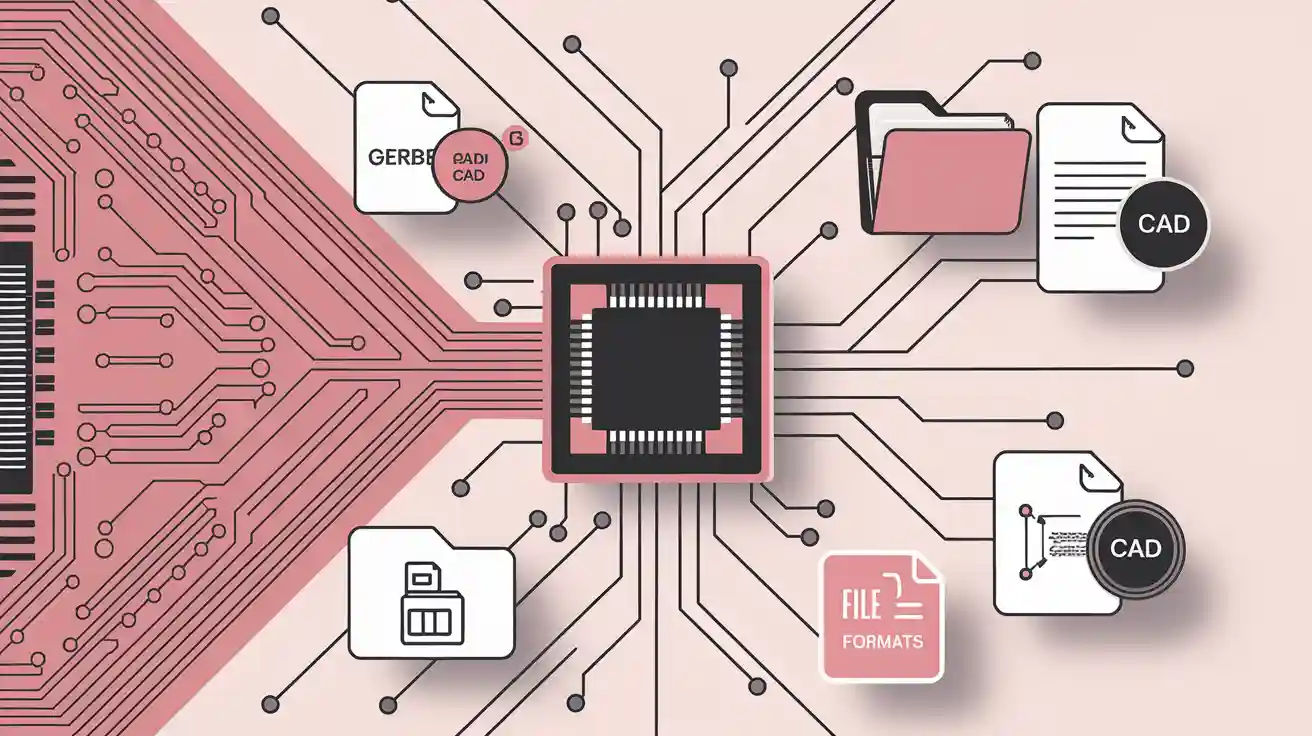
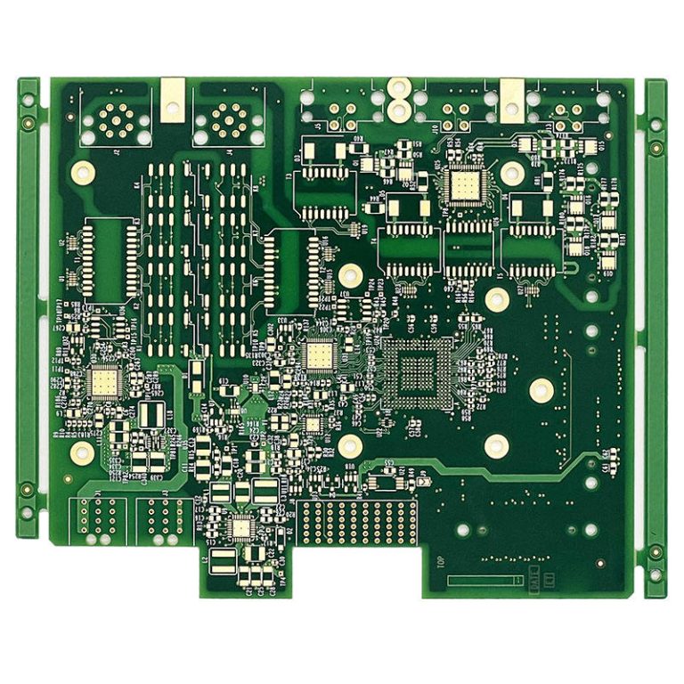
Printed Circuit Board (PCB) files are essential in electronics manufacturing. Common PCB file formats include Gerber, Excellon, ODB++, IPC-2581, BOM, and Pick-and-Place files. These PCB files ensure accurate communication of design and manufacturing details. Misaligned or incomplete PCB files can lead to incorrectly placed components, misrouted connections, and production delays, ultimately increasing costs and affecting PCB performance. Properly prepared PCB files streamline manufacturing processes, minimize errors, and improve quality control, making them indispensable for successful PCB production and assembly.
Key Takeaways
- Knowing PCB file types like Gerber and IPC-2581 is important. It helps designers and manufacturers work together better.
- Correct and complete PCB files lower mistakes and save time. They also improve quality checks.
- Advanced formats like ODB++ make manufacturing easier. They combine all needed data into one file.
- Checking files with tools like Gerber viewers avoids common errors. This ensures designs move smoothly to production.
- Keeping files clear and organized boosts efficiency. It also lowers the chance of expensive mistakes.
Importance of PCB File Formats
Role in PCB Design and Manufacturing
PCB file formats play a critical role in bridging the gap between design and manufacturing. These formats ensure that every detail of a PCB design is accurately communicated to manufacturers. For instance, Gerber X2 embeds essential metadata, reducing the risk of misinterpretation during production. This feature allows manufacturers to interpret designs quickly without requiring additional documentation, streamlining the workflow and minimizing errors.
The introduction of IPC-2581 in 2004 further revolutionized the process. This format eliminated conflicting documentation by enabling bidirectional communication between designers and manufacturers. It also allowed specific data to be sent to different parts of the supply chain, reducing unnecessary information transfer. By automating data loading into CAM systems, IPC-2581 minimized human error and accelerated the design-to-manufacturing process.
Case studies highlight the importance of PCB files in improving data accuracy and cycle times. For example, an ERP implementation project at a PCB manufacturer demonstrated how well-defined tasks and departmental cooperation, supported by accurate PCB file formats, enhanced overall efficiency. These examples underscore the indispensable role of PCB file formats in ensuring a seamless transition from design to production.
Impact on Assembly and Quality Control
Accurate PCB file formats are essential for successful assembly and quality control. They provide precise instructions for placing components, drilling holes, and routing connections. Errors in these files can lead to misplaced components or misaligned drill holes, which compromise the functionality of the final product.
Gerber X2 and ODB++ formats are particularly effective in reducing assembly errors. Gerber X2 includes metadata that ensures components are placed correctly, while ODB++ consolidates all design data into a single file, simplifying the assembly process. These formats enable manufacturers to detect potential issues early, reducing rework and improving product quality.
Reverse engineering of PCBs also highlights the importance of accurate file formats. This process assesses design and functionality, ensuring that the PCB meets quality standards. It also helps detect patent infringement, which can impact manufacturing. By providing a clear blueprint for assembly, PCB file formats enhance quality control and ensure that the final product meets design specifications.
Consequences of Incorrect or Incomplete Files
Incorrect or incomplete PCB files can have severe consequences for manufacturing and assembly. Missing layers, misaligned drill data, or incomplete component lists can lead to production delays and increased costs. These issues often require additional communication between designers and manufacturers, slowing down the workflow.
For example, if a Gerber file lacks critical metadata, manufacturers may misinterpret the design, resulting in defective PCBs. Similarly, incomplete BOM or Pick-and-Place files can cause assembly errors, such as missing or incorrectly placed components. These mistakes not only affect the functionality of the PCB but also damage the manufacturer’s reputation.
To avoid these problems, designers must ensure that all files are accurate and complete before submission. Using advanced formats like IPC-2581 and ODB++ can help reduce errors by consolidating data and automating processes. Proper preparation and verification of PCB files are essential for avoiding costly mistakes and ensuring a smooth manufacturing process.
Gerber File Preparation and Features
Overview of Gerber format
The Gerber file format is the industry standard for communicating PCB design data to manufacturers. It serves as a blueprint, detailing the layout of copper layers, solder masks, silkscreens, and other essential elements of a PCB. Originally developed as the RS274D format, it evolved into the more advanced RS274X format, which includes embedded aperture definitions. This advancement eliminated the need for separate aperture files, simplifying the manufacturing process.
Manufacturers rely on Gerber files to interpret design specifications accurately. These files ensure that every layer of the PCB is fabricated precisely as intended. The introduction of the Gerber X2 format further enhanced this process by incorporating metadata, such as layer functions and file attributes. This metadata reduces the likelihood of errors and improves communication between designers and manufacturers.
Key features of Gerber files
Gerber files offer several key features that make them indispensable for PCB manufacturing:
- Layer-specific data: Each Gerber file corresponds to a specific layer of the PCB, such as copper, solder mask, or silkscreen. This separation ensures clarity and precision during fabrication.
- Embedded aperture definitions: The RS274X format includes aperture definitions within the file, eliminating the need for external aperture lists. This feature streamlines the manufacturing process and reduces the risk of errors.
- Metadata integration: The Gerber X2 format adds metadata to describe layer functions, polarity, and other attributes. This enhancement improves data interpretation and reduces miscommunication.
- Compatibility with CAM tools: Gerber files are compatible with most Computer-Aided Manufacturing (CAM) software, allowing manufacturers to visualize and verify designs before production.
These features contribute to the widespread adoption of the Gerber file format in the PCB industry. Tools like Gerber viewers enable designers and manufacturers to review and validate files, ensuring that the final product meets design specifications.
Common issues with Gerber file preparation
Despite its advantages, Gerber file preparation can present challenges. Errors in these files can lead to manufacturing defects, delays, and increased costs. The following table highlights some common issues, their potential causes, and solutions:
| Issue | Potential Cause | Solution |
|---|---|---|
| Missing Aperture Data | Aperture definitions not included or incorrect | Check and validate aperture file alongside Gerber files |
| Layer Misalignment | Incorrect layering of copper, solder mask, etc. | Use Gerber viewer to align and validate layers |
| Inconsistent Drill Hole Sizes | Drill file inconsistencies or missing holes | Verify and cross-check drill files using verification tools |
Another table illustrates the impact of common mistakes and how to avoid them:
| Common Mistake | How to Avoid It | Impact of the Mistake |
|---|---|---|
| Missing drill files | Ensure drill files are clearly defined with accurate hole sizes and locations | Without drill files, manufacturers can’t place vias or holes correctly, leading to delays |
| Incomplete BOM | Double-check that all components are listed with correct part numbers and descriptions | Inaccurate BOMs can result in component shortages or incorrect part sourcing |
| Incorrect layer definitions | Use reliable DFM tools to validate all layers (copper, mask, paste, etc.) | Missing or incorrect layers can result in a non-functional PCB or misaligned components |
Proper Gerber file preparation minimizes these issues. Verification tools, such as Gerber viewers, play a crucial role in detecting errors early. These tools allow designers to preview files, ensuring that all layers align correctly and that no critical data is missing. Thorough preparation and validation of Gerber files significantly reduce the risk of manufacturing defects, ensuring a smooth production process.
Excellon and Drill Data Formats
Purpose of Excellon files
Excellon files play a vital role in PCB manufacturing by defining the size, location, and type of holes required for the board. These files guide drilling machines to create precise holes for vias, mounting points, and component leads. The Excellon format has become the industry standard for drill files due to its compatibility with most PCB drilling equipment. This ensures a seamless transition from design to production.
Accurate drill files are essential for maintaining the alignment and functionality of a PCB. Misaligned holes can lead to misplaced components or non-functional boards. By providing precise instructions, Excellon files help manufacturers avoid these issues and ensure the board meets design specifications.
Features of drill data formats
Drill data formats, including Excellon, offer several features that make them indispensable for PCB production:
- Hole size and location definition: Drill files specify the exact diameter and position of each hole, ensuring precision during manufacturing.
- Machine compatibility: The Excellon format works with most drilling machines, streamlining the production process.
- Layer-specific data: Drill files often include information about which PCB layer each hole corresponds to, aiding in accurate fabrication.
These features highlight the importance of drill files in achieving high-quality PCBs. Manufacturers rely on these files to produce boards that meet design and functionality requirements.
Common challenges with drill data
Despite their importance, drill files can present challenges during preparation and manufacturing. Common issues include:
| Challenge | Cause | Solution |
|---|---|---|
| Misaligned holes | Errors in drill file coordinates | Use verification tools to cross-check hole positions |
| Inconsistent hole sizes | Incorrect or missing size definitions | Validate drill files to ensure all hole sizes are accurately specified |
| File format compatibility | Outdated or unsupported drill file formats | Convert files to the Excellon format for compatibility with modern machines |
Inaccuracies in drill files can disrupt the manufacturing process, leading to delays and increased costs. For example, a missing or incorrect hole size can prevent components from being mounted properly. To avoid these issues, designers should verify drill files thoroughly before submission. Tools like CAM software can help detect and correct errors early, ensuring a smooth production process.
ODB++ Format for PCB Manufacturing
Overview of ODB++ format
ODB++ is a comprehensive file format designed to streamline PCB fabrication. It consolidates all necessary data into a single, unified database. Unlike traditional formats like Gerber, which require multiple files for different layers and processes, ODB++ simplifies communication by including all fabrication and assembly information in one package. This format supports multilayer PCB fabrication, making it ideal for complex designs.
Manufacturers benefit from ODB++ because it reduces the risk of errors during data transfer. The format includes detailed information about copper layers, drill data, solder masks, and even component placements. This level of detail ensures that manufacturers can produce PCBs exactly as intended by the designer.
Advantages of ODB++ over other formats
ODB++ offers several advantages over traditional formats like Gerber, particularly in terms of efficiency and error reduction. The following table highlights key differences:
| Feature/Benefit | ODB++ | Gerber |
|---|---|---|
| Completeness of data | Complete database of manufacturing info | Multiple files required |
| Error reduction | Less chance of error in data transfer | Higher chance of errors due to manual work |
| Automation facilitation | Encourages design and manufacturing automation | Manual intervention needed |
| Information included | All fabrication and assembly info included | Limited to image data |
| Access to data | Quick and easy access for manufacturers | Slower access due to multiple files |
| Design history continuity | Greater continuity and tracking | Less continuity due to manual processes |
ODB++ simplifies multilayer PCB fabrication by reducing manual intervention. Its ability to consolidate data into a single file minimizes the chances of miscommunication between designers and manufacturers. Additionally, the format supports automation, which accelerates production and improves accuracy.
Use cases for ODB++ in manufacturing
ODB++ is widely used in PCB fabrication and assembly due to its versatility. It is particularly beneficial for multilayer PCB fabrication, where precise alignment of layers is critical. Manufacturers rely on ODB++ to streamline processes such as drilling, solder mask application, and component placement.
This format also facilitates design validation. By including all necessary data in one file, ODB++ allows manufacturers to quickly verify designs before production begins. This reduces the likelihood of costly errors and ensures that the final product meets quality standards.
In high-volume production, ODB++ enhances efficiency by supporting automated workflows. Its comprehensive data structure enables seamless integration with modern manufacturing equipment, reducing setup times and improving throughput. For these reasons, ODB++ has become a preferred choice for PCB fabrication in industries ranging from consumer electronics to aerospace.
IPC-2581 Format for PCB Design
Overview of IPC-2581 format
IPC-2581 is an open, vendor-neutral file format designed to streamline the transfer of PCB design data from CAD tools to manufacturing systems. Unlike traditional formats like Gerber, which focus on image data, IPC-2581 consolidates all design, fabrication, and assembly information into a single file. This comprehensive approach eliminates the need for multiple files and reduces the risk of miscommunication during the manufacturing process.
The format supports advanced features such as embedded attributes, which provide detailed instructions for manufacturers. These attributes include layer functions, material specifications, and assembly details. By offering a standardized method for data exchange, IPC-2581 ensures consistency and accuracy across the entire PCB production workflow.
Benefits of IPC-2581 for design and manufacturing
IPC-2581 offers several advantages for both PCB designers and manufacturers. Its ability to integrate all necessary data into one file simplifies the handoff process, reducing errors and improving efficiency. For example, a recent revision of IPC-2581 (version B) introduced extensive attributes that allow manufacturers to interpret design intent more precisely. This improvement addresses limitations found in older formats like Gerber.
Industry research highlights the tangible benefits of adopting IPC-2581. The following table illustrates how companies have leveraged this format to overcome challenges and achieve better results:
| Company | Challenge | Result |
|---|---|---|
| Company A | Handoff of PCB design data using multiple proprietary formats | Reduced errors by 80% and cut time-to-market by 25% |
| Company B | Lack of standardized data exchange format affecting collaboration | Enhanced collaboration, improved quality, and a 15% reduction in manufacturing costs |
These examples demonstrate how IPC-2581 enhances collaboration, reduces costs, and accelerates production timelines.
Comparison with Gerber and ODB++
IPC-2581 stands out when compared to other PCB file formats like Gerber and ODB++. Each format has unique characteristics, but IPC-2581 offers distinct advantages:
- IPC-2581 serves as a comprehensive CAD-to-CAM data transfer format, while Gerber primarily functions as an image file format.
- ODB++ provides an integrated approach, which simplifies manufacturing processes. However, IPC-2581 surpasses ODB++ by offering a vendor-neutral standard that promotes broader industry adoption.
- Gerber’s limitations in accurately rendering design intent highlight the strengths of IPC-2581. The inclusion of extensive attributes in IPC-2581 ensures precise manufacturing expectations, addressing gaps in older formats.
By consolidating data and supporting advanced features, IPC-2581 provides a robust solution for modern PCB design and manufacturing needs.
PCBA File Formats: BOM and Pick-and-Place
Importance of BOM files
The Bill of Materials (BOM) file is a cornerstone of PCB assembly. It lists all components required for manufacturing, including part numbers, quantities, and descriptions. Manufacturers rely on BOM files to source materials and ensure accurate assembly. A well-prepared BOM file reduces the risk of missing components, which can delay production and increase costs.
BOM files also play a critical role in quality control. They provide a reference for verifying that the correct components are used during assembly. Errors in the BOM file, such as incorrect part numbers or missing items, can lead to defective PCBs. Designers must ensure that BOM files are complete and accurate to avoid these issues.
Role of Pick-and-Place files in assembly
Pick-and-Place files guide automated machines in placing components onto the PCB. These files contain precise coordinates for each component, ensuring accurate placement during assembly. Modern pick-and-place systems use advanced algorithms to achieve micron-level accuracy, which is essential for maintaining signal integrity and overall PCB performance.
Misalignment during assembly can cause signal interference, reducing processing efficiency and compromising the functionality of the PCB. Pick-and-Place files help prevent these issues by providing detailed instructions for component placement. Manufacturers use these files to optimize assembly processes and achieve high-quality results.
Key performance data highlights the importance of Pick-and-Place files:
- AI-driven pick-and-place systems achieve micron-level accuracy in PCB assembly.
- Precise placement of components is crucial for maintaining signal integrity and overall performance.
- Misalignment can lead to signal interference, which reduces processing efficiency.
Ensuring accuracy in PCBA file formats
Accuracy in PCBA file formats is vital for successful PCB assembly. Designers must verify that BOM and Pick-and-Place files contain complete and correct information. Missing or incorrect data can disrupt the manufacturing process, leading to delays and increased costs.
To ensure accuracy, designers should use software tools to validate PCBA file formats before submission. These tools can detect errors and inconsistencies, allowing designers to correct them early. Organizing files systematically and submitting them in the required format further streamlines the manufacturing process.
By prioritizing accuracy and completeness, designers can minimize errors and ensure a smooth transition from design to production. Proper preparation of PCBA file formats enhances efficiency and improves the quality of the final product.
Best Practices for Preparing PCB Files
Ensuring file accuracy and completeness
Accurate and complete PCB file preparation is essential for efficient manufacturing. Designers must ensure that every file includes all necessary details, such as layer definitions, drill data, and component placements. Missing or incorrect information can disrupt the workflow and lead to costly errors. Conducting rigorous Design Rule Checking (DRC) throughout the layout validates spacing and size constraints, ensuring manufacturability.
Footprint standardization simplifies the reuse of high-speed placement equipment and facilitates salvaging components. Incorporating dedicated test points into the design aids electrical verification without removing components. These practices enhance the reliability of the PCB and streamline the production process. Clear documentation, including assembly drawings and BOMs, prevents relearning efforts and guides the build process effectively.
Verifying compatibility with manufacturers
Compatibility between PCB files and manufacturing systems ensures a smooth workflow. Designers should confirm that their files align with the capabilities of the chosen manufacturer. For example, verifying drill file formats and layer specifications avoids miscommunication during production. Using standardized formats like IPC-2581 or ODB++ further reduces errors by consolidating data into a single file.
Accessibility plays a crucial role in compatibility. Sufficient clearance around components simplifies inspection and repair processes, accommodating variations in manufacturing equipment. Prioritizing Design for Manufacturing (DFM) from the start leads to robust designs that adhere to cost and schedule requirements. Collaboration with manufacturers during the design phase helps identify potential issues early, ensuring a seamless transition from design to production.
Organizing and submitting files effectively
Organized file submission accelerates the manufacturing process and minimizes errors. Designers should group files logically, ensuring that each file is labeled clearly and corresponds to its intended purpose. For instance, separating Gerber files by layer and including drill data in a dedicated folder simplifies interpretation.
Providing clear assembly drawings and BOMs ensures that manufacturers can quickly source components and begin assembly. Utilizing snap-fits and press-fits standardizes assembly and accommodates variations, further streamlining the workflow. Submitting files in widely accepted formats, such as Gerber or IPC-2581, ensures compatibility with most manufacturing systems. By organizing files systematically, designers enhance efficiency and reduce the likelihood of production delays.
Common Errors in PCB Files and How to Avoid Them
Missing or Incorrect Layers
Missing or incorrect layers in PCB files can lead to significant manufacturing issues. Each layer serves a specific purpose, such as defining copper traces, solder masks, or silkscreens. If a layer is missing or improperly defined, the PCB may fail to function as intended. For example, an absent solder mask layer can expose copper traces, increasing the risk of short circuits.
To avoid these errors, designers should use tools like Gerber viewers to validate layer definitions before submission. These tools allow users to preview each layer, ensuring alignment and completeness. Organizing layers systematically and labeling them clearly also reduces the likelihood of mistakes. File formats like IPC-2581 simplify this process by consolidating all layer data into a single file, improving accuracy and streamlining communication with manufacturers.
Misaligned Drill and Design Data
Misaligned drill and design data disrupt the manufacturing process and compromise PCB functionality. Misalignment can cause vias and mounting holes to deviate from their intended positions, leading to connectivity issues or component placement errors.
Several quality control measures help identify and prevent these issues:
- Validate drill files to ensure accuracy before manufacturing.
- Use Design for Manufacturing (DFM) checks to verify hole sizes and layer alignment.
- Conduct visual inspections using a Gerber viewer to simulate drilling processes.
- Verify tool sizes against specifications to prevent misalignment.
- Perform precise coordinate checks to ensure alignment with the PCB layout.
Modern file formats like ODB++ and IPC-2581 integrate design, assembly, and testing data into a single file. This comprehensive approach minimizes errors and misalignments, leading to quicker production times and higher-quality results.
Incomplete BOM or Pick-and-Place Files
Incomplete BOM or Pick-and-Place files disrupt PCB assembly and increase production costs. A missing component in the BOM file can delay sourcing, while incorrect coordinates in Pick-and-Place files can lead to misplaced components. These errors compromise the PCB’s functionality and require costly rework.
To ensure accuracy, designers must double-check BOM files for completeness, including part numbers, quantities, and descriptions. Pick-and-Place files should be validated using software tools to confirm coordinate accuracy. Organizing PCBA file formats systematically and submitting them in widely accepted formats, such as IPC-2581, further reduces errors.
By prioritizing accuracy and completeness in PCBA file formats, designers can streamline assembly processes and improve the quality of the final product.
Proper preparation of PCB files plays a pivotal role in ensuring successful manufacturing and assembly. Each file type, from Gerbers to BOMs, carries critical information that guides fabricators and assemblers. Effective communication between designers and manufacturers minimizes errors, reduces delays, and ensures the PCB is built as intended.
Adherence to industry standards and thorough file verification are essential steps in this process. Missing or inaccurate data can lead to costly mistakes and production setbacks. By prioritizing precision and providing all necessary documentation, designers can streamline workflows and achieve high-quality results.
📌 Tip: Always validate your files and confirm compatibility with your manufacturer to avoid unexpected issues.
FAQ
What are PCB files, and why are they important?
PCB files contain the design and manufacturing data for printed circuit boards. They guide manufacturers in fabricating and assembling PCBs accurately. These files ensure that every detail, from copper traces to component placements, is communicated effectively, reducing errors and improving production efficiency.
How does the Gerber format differ from ODB++?
Gerber files focus on layer-specific image data, requiring multiple files for a single PCB. ODB++ consolidates all design, fabrication, and assembly data into one file, simplifying communication and reducing errors during manufacturing.
What is the role of a BOM file in PCB assembly?
A BOM file lists all components required for PCB assembly, including part numbers, quantities, and descriptions. It ensures accurate sourcing and placement of components, minimizing delays and errors during production.
Why is file accuracy critical in PCB manufacturing?
Accurate files prevent manufacturing errors like misaligned layers or missing components. They ensure that the PCB functions as intended and reduce costly rework or delays. Verification tools help designers check file accuracy before submission.
How can designers avoid common errors in PCB files?
Designers can use tools like Gerber viewers and DFM checks to validate files. Organizing files systematically and using standardized formats like IPC-2581 or ODB++ also minimizes errors and ensures compatibility with manufacturers.