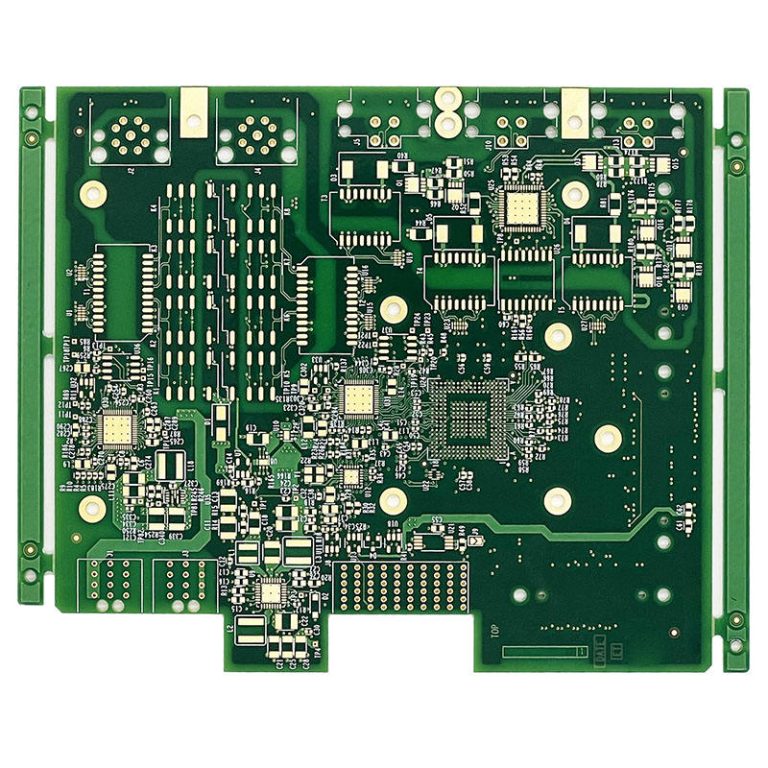
How to Master BGA Assembly for Reliable PCB Connections

Precision is the cornerstone of successful BGA assembly. Every step, from solder paste application to reflow, demands strict process control to avoid costly errors. When you master this process, you ensure that your PCB connections remain robust and reliable, even in demanding environments.
BGA technology offers several advantages, including compact designs, excellent thermal performance, and high pin density. However, challenges like solder bridging, voids, and inspection difficulties require your attention and expertise. Overcoming these obstacles will help you unlock the full potential of BGA assemblies in modern electronics.
Key Takeaways
- To master BGA assembly, follow strict steps for strong PCB links.
- Plan your PCB layers by checking paths and adding power and ground layers.
- Pick the best solder paste and stencil to apply solder correctly and avoid mistakes.
- Do careful checks, like X-rays and tests, to make sure hidden solder joints are good.
- Fix issues like solder bridges and gaps by improving solder use and heating steps.
Basics of BGA Assembly
Role of BGA in PCB Manufacturing
Ball Grid Array (BGA) technology plays a pivotal role in modern PCB manufacturing. It enables compact designs by offering high pin density, which is essential for devices requiring advanced functionality in limited space. You can use BGA components to achieve efficient power and ground connections, as they often dedicate multiple pins to these functions. This design approach simplifies the integration of power rails on plane layers, ensuring stable electrical performance.
When planning a PCB layout, placing the largest BGA component first helps streamline floorplanning. This decision influences layer count and routing strategies, especially for high-speed signals. Reliable routing paths must be established to avoid issues like crosstalk, which can compromise signal integrity. By leveraging BGA technology, you can optimize PCB designs for performance and scalability.
Advantages of BGA Technology
BGA technology offers several advantages that make it a preferred choice for PCB assembly. Its compact design allows for smaller and lighter devices, which are critical in industries like consumer electronics and aerospace. The high pin density of BGA components supports complex routing configurations, enabling advanced functionality without increasing the PCB size.
Thermal performance is another key benefit. BGA packages dissipate heat more effectively than traditional leaded components, reducing the risk of overheating. This feature is particularly valuable in applications requiring high power or continuous operation. Additionally, BGA components improve electrical performance by minimizing inductance and resistance in connections, ensuring reliable signal transmission.
Challenges in BGA Assembly
Despite its advantages, BGA assembly presents unique challenges. The hidden solder joints beneath the component make inspection difficult, requiring specialized tools like X-ray imaging. Solder bridging and voids are common issues during reflow, which can lead to unreliable connections. You must carefully optimize the reflow profile to mitigate these risks.
Routing for BGA components demands precision. High-speed signals require controlled impedance and adequate spacing to prevent interference. Determining exit routes for traces can be complex, especially in dense layouts. Additionally, handling large BGAs requires strict protocols to avoid physical damage during assembly. Addressing these challenges ensures the reliability and longevity of your PCB designs.
Effective BGA Design Strategies
PCB Layer Stack Optimization
Optimizing the PCB layer stack is essential for achieving reliable BGA design performance. You can start by analyzing the routing requirements of your BGA components. Typically, the first two outer rows of a BGA device do not require vias, allowing you to route these connections on the surface layer. This strategy helps determine the total number of layers needed for signal fanout while maintaining effective isolation between ground and signal layers.
To enhance PCB layout efficiency, consider implementing multi-layer designs with dedicated ground and power planes. These layers improve electrical stability and reduce noise interference. Proper spacing between signal traces minimizes crosstalk, ensuring clean signal transmission. Additionally, impedance matching techniques help maintain consistent signal integrity, especially for high-speed applications.
Key strategies for layer stack optimization include:
- Minimizing crosstalk by spacing signal traces appropriately.
- Designing traces for impedance matching to improve signal quality.
- Using differential pair routing for high-speed signals.
- Shortening critical traces to reduce latency and interference.
Signal Layer and Fanout Considerations
Effective routing is the backbone of successful BGA design. You must carefully plan signal layers and fanout strategies to avoid bottlenecks in high-density PCB layouts. BGA escape routing, which involves routing signals from the inner rows of the BGA package, requires precision to prevent overlapping or interference.
For high-speed signals, controlled impedance routing is critical. You can achieve this by maintaining consistent trace widths and spacing. Differential pair routing is another effective method for high-speed applications, as it reduces electromagnetic interference and enhances signal integrity. Shorter traces for critical connections further improve design performance.
When planning fanout, prioritize routing paths that minimize signal distortion. Use vias strategically to transition signals between layers without compromising performance. By optimizing signal layers and fanout, you ensure reliable connections and robust PCB functionality.
Thermal Management in BGA Design
Thermal management plays a vital role in maintaining the performance and reliability of BGA designs. High-density PCB applications generate significant heat flow density, which can lead to component failure if not managed effectively. You must incorporate robust thermal dissipation strategies to address this challenge.
Start by conducting a thorough thermal analysis during the design phase. Identify heat conduction paths and implement cooling techniques such as heat sinks or thermal vias. These methods help dissipate heat away from critical components, ensuring stable operation.
Increasing assembly density requires innovative approaches to meet thermal requirements. For example, optimizing the placement of heat-generating components and using materials with high thermal conductivity can improve overall heat management. By prioritizing thermal considerations, you safeguard your PCB against overheating and enhance its long-term reliability.
Reliable BGA Soldering Techniques
Choosing the Right Solder Paste
Selecting the appropriate solder paste is critical for successful bga soldering. The paste serves as the adhesive and electrical connection medium between the bga component and the pcb. You must evaluate the paste’s composition, viscosity, and particle size to ensure compatibility with your assembly process.
For bga assembly, lead-free solder paste is often preferred due to environmental regulations. However, leaded options may still be used in specific applications requiring lower melting points. The flux type in the solder paste also plays a significant role. No-clean flux reduces post-soldering cleaning requirements, while water-soluble flux offers superior cleaning results for high-reliability applications.
When performing solder paste selection, consider the reflow temperature profile of your assembly. The paste must withstand the thermal cycles without degrading. Additionally, ensure the paste’s shelf life and storage conditions align with your production schedule to maintain consistent quality.
Stencil Design for Solder Paste Application
The stencil design directly impacts the accuracy of solder paste deposition during bga soldering. A well-designed stencil ensures uniform paste application, reducing the risk of defects like solder bridging or insufficient solder volume.
You should select a stencil thickness that matches the pitch and ball size of the bga package. For fine-pitch components, thinner stencils provide better control over paste volume. Laser-cut stencils with electro-polished apertures offer superior precision, ensuring consistent paste deposition.
Aperture design is equally important. Rounded or trapezoidal apertures minimize paste sticking, improving release during the printing process. For bga components, you may need to use reduced aperture sizes to prevent excessive paste application, which can lead to solder voids during reflow.
Proper alignment of the stencil with the pcb is crucial. Misalignment can cause uneven paste distribution, leading to connectivity issues. Regularly inspect and clean the stencil to maintain its performance throughout the assembly process.
Reflow Profile Optimization
Reflow profile optimization is the cornerstone of reliable bga soldering. The reflow process involves heating the pcb and bga components to melt the solder paste, forming robust electrical and mechanical connections. You must carefully control the temperature profile to avoid defects like solder bridging, voids, or component damage.
A typical reflow profile consists of four stages: preheat, soak, reflow, and cooling. During the preheat stage, the temperature gradually rises to activate the flux and reduce thermal shock. The soak stage ensures uniform heating across the pcb, preparing the solder paste for melting.
The reflow stage is the most critical. The temperature must exceed the solder paste’s melting point without exceeding the thermal limits of the bga components. Use a reflow oven with precise temperature control to achieve consistent results. Finally, the cooling stage solidifies the solder joints, ensuring their strength and reliability.
To optimize the reflow profile, monitor the thermal behavior of your pcb using thermocouples or thermal imaging. Adjust the heating and cooling rates to minimize stress on the components. By fine-tuning the reflow process, you can enhance the quality and durability of your bga assembly.
Inspection and Validation for BGA Assembly
X-ray Inspection for Hidden Joints
X-ray inspection is an essential step in verifying the integrity of hidden solder joints in BGA components. Since the solder balls are located beneath the package, traditional inspection methods cannot detect defects like voids, bridging, or insufficient solder. You can use X-ray imaging to visualize these hidden connections and ensure they meet quality standards.
Advanced X-ray systems allow you to analyze solder joint quality in real-time. These systems provide high-resolution images that reveal internal defects, enabling you to identify and address issues early in the process. By incorporating X-ray inspection into your post-reflow inspection workflow, you can significantly improve the reliability of your PCB assemblies.
Electrical Testing for Reliability
Electrical testing ensures that your BGA assembly performs as intended. This process involves verifying the electrical continuity and functionality of the solder joints. You can use in-circuit testing (ICT) or functional testing to evaluate the performance of your PCB.
ICT checks for open circuits, short circuits, and other connectivity issues. Functional testing, on the other hand, simulates the operating conditions of the PCB to confirm its performance. Both methods help you validate the quality of BGA solder joints and ensure the assembly meets design specifications. Regular electrical testing minimizes the risk of field failures and enhances product reliability.
Visual Inspection for Surface Defects
While X-ray and electrical testing focus on hidden and functional aspects, visual inspection addresses surface-level defects. You should examine the PCB for issues like solder splatter, misaligned components, or damaged traces. These defects can compromise the overall quality of your assembly if left unaddressed.
Use magnification tools to inspect the surface of the PCB thoroughly. Pay close attention to the alignment of the BGA package and the cleanliness of the solder joints. A clean and defect-free surface contributes to the durability and performance of the assembly. Combining visual inspection with other validation methods ensures a comprehensive quality control process.
Solving Common BGA Assembly Challenges
Rework Strategies for Defective Components
Reworking defective BGA components requires precision and a well-defined process. You must first identify the defective component using inspection methods like X-ray imaging or electrical testing. Once identified, carefully remove the component without damaging the surrounding PCB area. A hot air rework station or an infrared rework system can help you achieve this.
After removal, clean the PCB pads thoroughly to eliminate residual solder or flux. Use a solder wick or a vacuum desoldering tool for this step. Proper cleaning ensures a smooth surface for reattachment. Next, apply fresh solder paste to the pads using a stencil for accurate deposition.
When placing the new BGA component, use vision-assisted placement equipment to ensure precise alignment. Reflow the assembly using a profile that matches the solder paste and component specifications. Monitor the reflow process closely to avoid overheating or misalignment. Finally, inspect the reworked area to confirm the integrity of the solder joints.
Tip: Always verify the coplanarity of the replacement BGA component before reattachment. This ensures all solder balls make proper contact with the PCB pads.
Handling Protocols to Prevent Damage
Proper handling protocols are essential to prevent damage during BGA assembly. You should store components and PCBs in a controlled environment to protect them from moisture and contaminants. Moisture-sensitive level (MSL) handling procedures are particularly important for BGA components, as excess moisture can lead to defects during reflow.
Electrostatic discharge (ESD) protection is another critical aspect. Always use ESD-safe tools and workstations to avoid damaging sensitive components. When applying solder paste, ensure consistent deposition by using a high-quality stencil with an appropriate aperture design. Optimizing solder paste volume, typically 50-70% of the pad area, reduces the risk of solder bridging or voids.
During assembly, use vision-assisted placement equipment to ensure proper component orientation and alignment. Fiducial marks on the PCB can improve placement accuracy. Additionally, verify the flatness of the PCB and the coplanarity of the BGA component to ensure reliable connections.
Note: Implementing nitrogen reflow can reduce oxidation during the soldering process, further enhancing the quality of your assembly.
Addressing Solder Bridging and Voids
Solder bridging and voids are common issues in BGA assembly, but you can address them with careful process optimization. To prevent solder bridging, ensure accurate solder paste deposition. Use a stencil with reduced aperture sizes for fine-pitch components and maintain proper alignment during printing.
During reflow, optimize the temperature profile to minimize defects. Adequate preheat and soak times reduce thermal shock, while a controlled peak temperature ensures complete solder melting without overheating. Time above liquidus should be sufficient to allow the solder to flow evenly, reducing the likelihood of voids.
For void reduction, focus on solder paste quality and application. Consistent paste deposition and proper flux activation during reflow play a significant role. Additionally, using PCBs with tight flatness tolerances and ensuring proper pad design can improve solder joint reliability.
Tip: Conduct regular inspections and thermal profiling to identify and address process variations that may contribute to solder defects.
Mastering BGA assembly requires a combination of strategic design, precise soldering, and thorough inspection. By adhering to IPC standards and leveraging advanced inspection methods, you can ensure reliable outcomes. For example, visual inspection identifies surface defects like cracks or misalignment, while X-ray imaging detects voids in solder balls. The table below highlights key inspection criteria:
| Inspection Method | Criteria for Reliable Assembly Outcomes |
|---|---|
| Visual Inspection | Inspect for wetting, remnant flux, cracks, shorting, and alignment of pin ‘1’. |
| X-ray Inspection | Check for voiding in solder balls, with specific criteria for collapsing and non-collapsing balls as per IPC-A-610. |
| IPC Standards | Adherence to IPC-A-610 and IPC-7095 for acceptance criteria and process validation ensures quality in BGA interconnections. |
Precision and process control are essential for achieving consistent results. By adopting these best practices, you can enhance the reliability and performance of your BGA assemblies.
FAQ
What is the most common cause of solder bridging in BGA assembly?
Solder bridging often occurs due to excessive solder paste application or misaligned stencils. You can prevent this by using a properly designed stencil with reduced aperture sizes and ensuring precise alignment during paste deposition.
Tip: Regularly inspect and clean your stencil to maintain consistent paste application.
How can you ensure reliable thermal management in BGA designs?
You can ensure effective thermal management by conducting a thermal analysis during the design phase. Use thermal vias, heat sinks, and high-conductivity materials to dissipate heat efficiently. Proper placement of heat-generating components also minimizes overheating risks.
Note: Always verify thermal performance under real-world operating conditions.
Why is X-ray inspection critical for BGA assembly?
X-ray inspection allows you to detect hidden defects like voids, bridging, or insufficient solder in BGA joints. These issues are invisible to the naked eye but can compromise the reliability of your assembly.
Emoji Insight: 🛠️ Advanced X-ray systems provide high-resolution images for precise defect analysis.
What is the best way to handle moisture-sensitive BGA components?
Store moisture-sensitive components in a controlled environment with proper humidity levels. Follow MSL (Moisture Sensitivity Level) guidelines and bake components if necessary before assembly to prevent defects during reflow.
Reminder: Use desiccant packs and vacuum-sealed packaging for long-term storage.
How do you optimize the reflow profile for BGA soldering?
Optimize the reflow profile by carefully controlling the preheat, soak, reflow, and cooling stages. Monitor the temperature to ensure it exceeds the solder paste’s melting point without damaging components.
Pro Tip: Use thermocouples or thermal imaging to validate your reflow process.