
 English
 Arabic
 Chinese (Simplified)
 Dutch
 French
 German
 Italian
 Portuguese
 Russian
 Spanish

Smart Socket PCBA and Assembly Process: From PCB to Functional Test
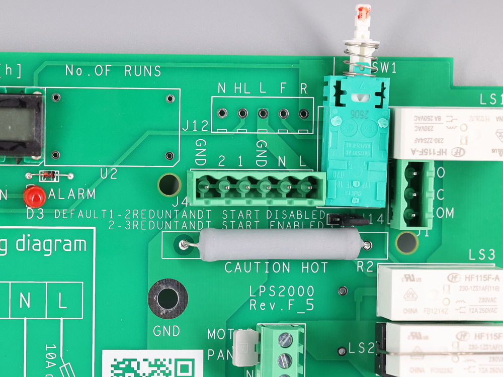
Introduction: The Rise of Smart Socket PCB Assembly
Smart sockets and smart plugs are rapidly transforming both consumer and commercial environments by enabling remote control, automation, and real-time energy monitoring for almost any electrical appliance. At the heart of each Wi-Fi smart socket, Bluetooth socket, or Zigbee smart plug is a highly sophisticated smart socket PCB assembly—a miniature, high-reliability control board that manages power, connectivity, safety, and all intelligent features.
Why the Focus on Smart Socket PCB Assembly Today?
With the explosion of the smart home market—expected to reach $135 billion by 2025—smart socket manufacturing and smart plug PCB assembly process demand both innovation and precision. From the design of the control board, selection of components, and SMT and DIP assembly processes, to rigorous PCBA testing for safety and compliance, every step is critical. As devices must safely handle high currents, frequent switching, and operate in electromagnetically noisy environments, the challenges faced by smart socket manufacturers have become truly unique.
“In connected device manufacturing, the reliability, safety, and performance of the PCB assembly define product success.” — Carol Wang, Senior PCBA Design Engineer
Whether you are an IoT product designer, OEM buyer, or just curious about the technical heart of modern smart sockets, this guide provides a comprehensive, inside look at how smart socket circuit boards are designed, assembled, and tested to meet today’s exacting standards.
Key Facts At-A-Glance
| Feature | Smart Socket PCB Assembly | Advantage |
|---|---|---|
| Common Communication | Wi-Fi, Bluetooth, Zigbee, Matter | Seamless integration with smart home hubs |
| Main Control Component | MCU or Wi-Fi SoC | Enables wireless logic and control |
| High-Voltage Design | AC-to-DC power supply, relays, creepage focus | Safe power management, isolation |
| Energy Monitoring | Metering ICs, current sensors | Track energy usage, monitor safety |
| Testing Procedures | ICT, FCT, AOI, Hi-pot, Burn-in | Ensures reliability and compliance |
What Does a Smart Socket PCBA Do?
A smart socket PCBA (Printed Circuit Board Assembly) is the “brain” that powers intelligent smart sockets and plugs. This tiny but mighty module handles vital functions, making it possible to remotely control, automate, and monitor the energy use of almost any electrical load—lamps, fans, air conditioners, or office equipment—via smartphone apps or voice assistants.
Core Functions of Smart Socket Circuit Boards
1. Power Management and Conversion At its foundation, a smart socket circuit board needs to safely convert high-voltage AC (usually 110V or 230V depending on region) into multiple DC voltages to power logic and wireless chips. This step is performed by specialized AC-DC power supply circuits designed with extra tight creepage and clearance distances to comply with global safety standards such as IEC 60950 or UL 60730.
2. Wireless Connectivity The heart of the control board is typically a Wi-Fi, Bluetooth, or Zigbee module—a Wi-Fi SoC (System on Chip) or MCU (Microcontroller Unit) with integrated radio transceiver. This allows the smart socket to join home networks, support cloud services, and communicate with platforms like Alexa or Google Home.
3. Load Switching (Relay/Triac Control) The smart socket assembly switches appliances on and off by energizing an electromechanical relay or triac (for AC load control). Special consideration is required for high current paths and relay driver circuits to support frequent switching cycles—potentially thousands per year.
4. Energy Monitoring and Safety Protection Modern smart socket PCBs include current sensors and energy metering ICs to track consumption in real time. Many designs also integrate surge protection and built-in monitoring for temperature, overload, and earth-leakage faults, ensuring both user safety and product longevity.
Key Components Inside a Smart Socket PCBA
The complexity of a smart socket or smart plug circuit board is hidden under its compact shell. Let’s break down the essential smart socket components and their critical roles:
| Component | Functionality |
|---|---|
| MCU / Wi-Fi SoC | Main processor & connectivity—manages commands, schedules, updates, and wireless network logic |
| AC-DC Power Supply | Converts 110–230V AC to stable DC voltages for logic, relays, and LEDs |
| Electromechanical Relay or Triac | Switches AC loads (high current path), electrically isolated from logic circuitry |
| Energy Metering IC | Measures voltage, current, and calculates real-time power consumption and energy |
| Current Sensor | Detects load current, often for overload or short-circuit protection |
| Passive Components | Capacitors, resistors, inductors—signal conditioning, filtering, EMC/EMI compliance |
| High-Current Connectors/Terminals | Ensures safe connection from AC mains to internal PCB and output socket pins |
| Antenna / Wireless Module | Enables stable communication for Wi-Fi/Bluetooth/Zigbee/Matter |
| Indicator LEDs & Buttons | For user feedback and local reset/pairing |
Common Challenges in Smart Socket PCB Assembly
Smart socket PCB design and assembly face far greater challenges than the assembly of low-voltage or non-critical consumer devices due to both regulatory pressures and extreme electrical conditions.
Key Manufacturing and Design Challenges
1. Clearance and Creepage Distance Because AC lines and low-voltage logic must coexist on the same board, maintaining minimum creepage and clearance distances (the shortest air and surface distances between high-voltage traces) is vital. Even small mistakes or solder bridging can cause dangerous shorts or shocks.
| Voltage Range | Min. Creepage Distance (mm) | Min. Clearance (mm) |
|---|---|---|
| Up to 250V | 2.5 | 2.0 |
| 250V–400V | 4.0 | 3.0 |
2. Thermal Management for High-Current Traces Smart plug boards often must handle 10–16A loads. Copper weight of 2oz/ft² is common, with wide traces, thermal vias, and heat spreaders to prevent overheating, which can cause board delamination or failure.
3. High-Current Trace Design Careful layout is required to keep high-current paths short and isolated from sensitive signal traces, reducing losses and risk of arcing or EMC problems.
4. Electromagnetic Interference (EMI) Switching heavy loads, wireless radios, and power line surges can introduce EMI. The smart socket PCB design uses shielding, ferrite beads, and careful grounding to suppress noise and ensure both radio signal quality and safety.
5. Component Selection and Placement High-quality, certified relays and optoisolators (for control isolation) must be used; inadequate isolation or counterfeit parts can result in field failures, recalls, or even fires.
Smart socket quality assurance means identifying these challenges during design reviews, DFM (Design for Manufacturability) analysis, and in every step of production.
The Smart Socket PCB Assembly Process
Bringing a smart socket from schematic to finished, functioning device involves multiple tightly controlled manufacturing steps with thorough quality checks at each juncture. Here’s an in-depth walkthrough of the smart socket assembly process:
1. Solder Paste Printing & Inspection (SPI)
- Precise solder paste is printed only on pads intended for SMT components.
- SPI systems verify alignment, thickness, and coverage for every pad to prevent defects.
2. SMT Component Placement
- Pick-and-place robots position tiny resistors, capacitors, MCUs, relays, and connectors.
- Surface-mount technology (SMT) supports smaller, more reliable, and faster boards.
3. Reflow Soldering
- Assembled boards are conveyed through a reflow oven where solder melts, bonding components permanently to the PCB.
- Controlled thermal profiles are crucial to avoid cold solder joints or warping, especially near PCB edges or under large relays.
4. AOI & X-ray Inspection
- Automated Optical Inspection (AOI) scans for missing or misaligned parts, solder bridges, and polarity issues.
- X-ray inspection reveals hidden solder defects underneath BGAs or dense component clusters.
5. Through-Hole Insertion & Soldering (DIP/THT)
- High-current connectors, relays, and AC pins are inserted manually or by robot, then soldered using wave soldering.
- Sometimes selective soldering is used for precision—especially in mixed-technology assemblies.
6. Optional Conformal Coating
- A protective film is applied over the finished board for added moisture resistance and to prevent corrosion or accidental shorting.
7. Final Assembly, Labeling, and Traceability
- Each smart socket PCB is assembled into its case, labeled for traceability (batch and serial number), and prepared for final quality checks.
Pro-tip: Selecting an assembly partner that complies with IPC-A-610 standards is crucial for high-quality smart socket manufacturing, as these standards define acceptability for electronic assemblies.
How Smart Socket PCBAs Are Tested
Testing is arguably the most crucial phase in smart socket manufacturing. Rigorous, multi-layered smart socket PCBA testing ensures reliability, functionality, and, ultimately, user safety.
Main Testing Steps for Smart Socket Circuit Boards
1. In-Circuit Testing (ICT)
- Checks each soldered net, verifies component placement, orientation, and values. Open circuits, shorts, and misloads are detected early.
2. Automated Functional Testing (FCT)
- Simulates real use cases: the board is powered, connects to Wi-Fi/Bluetooth, relays switch, metering ICs report data, and response to commands is checked.
- Essential for verifying firmware and real-world behaviors.
3. High-Potential (Hi-Pot) / Dielectric Withstand Testing
- Applies high voltage between AC and logic domains to confirm correct isolation and prevent electrical shock hazards.
4. Burn-In and Environmental Stress Testing
- PCBs are operated under load in high/low temperature and humidity chambers for hours or days to expose latent defects.
5. Wireless Communication Testing
- Confirms ability to pair, maintain connection, and transmit data across actual signal ranges in various environments.
6. Relay Load and Endurance Testing
- Switches relays on/off under load thousands of times to uncover weak or faulty components.
7. Energy Metering Calibration
- Compares the board’s readings against precision reference meters to ensure accuracy of energy usage reporting.
| Testing Type | Target Issue |
|---|---|
| In-Circuit Testing (ICT) | Missing components, wrong values, solder bridges |
| Functional Testing (FCT) | Firmware bugs, faulty relay switching, user interface |
| Hi-Pot/Dielectric Testing | Inadequate isolation, risk of electrical shock |
| Burn-in/Stress Testing | Early-life failures, thermal instability |
| Wireless & Communication | Connectivity failures, antenna issues, dropouts |
| Energy Metering Calibration | Inaccurate energy or power readings |
Smart Plug PCB Assembly: From Prototype to Mass Production
The path from idea to fully released smart plug or smart socket involves several stages of PCB manufacturing and assembly. Each phase has its own priorities and risks.
1. Prototype Production
- Small batches (5–50 pieces) used to validate hardware, PCB layout, and firmware.
- Quick-turn PCB fab and hand or semi-automated SMT assembly allow for rapid design tweaks.
- Early testing (FCT, ICT, relay load) ensures that critical switching, energy monitoring IC, and Wi-Fi SoC functionalities perform as intended.
2. Quality Control Standards & Documentation
- Inspection checkpoints (AOI, X-ray) are documented at each stage.
- Compliance with IPC-A-610, UL/IEC safety, and local EMC standards is established early.
3. Low-Volume Production
- 100–500 units. More automated assembly, introduction of wave soldering for through-hole tech.
- First time full product traceability and batch QA cycles are implemented.
- DFM (Design for Manufacturability) reviews address any warping, soldering, or test yield issues.
4. Mass Production
- 1,000–1,000,000 units, highly automated pick-and-place, soldering, and test lines.
- Focus on smart plug PCB assembly traceability, defect prevention, and scalability without loss of quality.
- Final packaging, serialization, and drop-shipment to OEM or direct to retailers.
Table: Comparing Prototype and Mass Production Smart Socket PCBA Workflows
| Stage | Focus | Typical Volume | Assembly Process | Testing/QA |
|---|---|---|---|---|
| Prototype | Validation, Speed | 5–50 | Mixed (hand/auto) | FCT, ICT basic tests |
| Low Volume | DFM, Traceability | 100–500 | More automation | AOI, X-ray, FCT |
| Mass Production | Cost, Scale, Zero Defects | 1,000+ | Fully automated SMT/DIP | Automated, all stages |
Key Manufacturing Challenges in Smart Plug PCBA
As assembly volume grows, so do the potential pitfalls. Smart plug PCBA manufacturers must vigilantly address several pain points:
1. Relay Selection & High-Current Switching
- Relays must be rated at least +30% above intended maximum load (e.g., use 20A relays for 16A plugs).
- Life-cycle and surge testing are critical to prevent premature relay failure.
2. Wireless Communication Performance
- Poor PCB antenna layout leads to Wi-Fi/Bluetooth “dead spots” and higher returns.
- Shields, cutouts, and proper RF trace routing are a must in smart plug PCB design.
3. PCB Layout: High-voltage Isolation
- Misplaced or insufficient creepage and clearance can lead to catastrophic AC–DC shorts.
- Advanced smart socket circuit boards may opt for 4-layer PCBs to maximize separation and reliability.
4. Thermal Management
- Undersized PCB copper weight or traces may overheat, causing discoloration or PCB damage under sustained high current.
- Design rules:
- Use ≥2oz copper for line traces.
- Add “thermal reliefs” (wide traces/vias under relays, fusing for protection).
5. Assembly Defects and Prevention
- Common defects: Cold solder joints, misaligned components, tombstoning, solder bridges.
- Prevention: AOI/X-ray for every board, traceability, and post-reflow inspection logs.
Quick quote from procurement manager: “We select smart socket PCB assembly partners not only by price, but by demonstrated test pass rates, relay sourcing, and real field defect statistics.”
How to Choose a Reliable Smart Socket/Plug PCBA Manufacturer
Choosing the right smart socket PCBA contract manufacturing partner is as important as your initial design. Here’s a checklist to guide your selection:
1. SMT and DIP Capabilities
- Do they support both surface-mount technology (SMT) and through-hole assembly (DIP/THT) in-house?
- Can they handle relays, AC connectors, thick copper, and mixed-technology PCBs without outsourcing?
2. Experience with High-Voltage, Mains-Powered Devices
- Proven track record with smart plug circuit board assembly or similar IoT products?
- Experience with international safety and EMC certifications for Europe, North America, and beyond?
3. Full Testing and Quality Management
- In-house FCT, ICT, AOI, X-ray, and Hi-pot testing for every board?
- Do they maintain test logs, batch QA, and root-cause analysis for failures?
4. Engineering and DFM (Design For Manufacturability) Support
- Can they review your smart socket PCB design files for manufacturability and suggest improvements?
- Will they offer BOM sourcing, substitution, or redesign advice during the quotation process?
5. Traceability and Documentation
- Can every board be tracked by lot number, serial, and date code—crucial for regulatory compliance and warranty management?
FAQs
1. What’s hidden inside a smart socket?
A smart socket contains a control board with a Wi-Fi/Bluetooth SoC, AC-to-DC power supply, relay/triac, energy metering IC, current and thermal sensors, and RF antenna—the core of all its intelligence and safety.
2. What copper weight and PCB thickness are recommended for high-current smart sockets?
For 10A–16A smart plugs, use PCB copper weight ≥2oz/ft² and thickness ≥1.6mm to prevent overheating and ensure durability.
3. Why do clearance and creepage distances matter in smart socket circuit boards?
They prevent arcing and dangerous shorts between AC and DC domains. Regulatory failures here can cause unsafe products and costly recalls.
4. What is the difference between SMT and THT (DIP) assembly for smart socket boards?
SMT places components directly onto PCB surfaces, allowing higher density and automation. DIP/THT is used for heavy duty or high-power parts (relays, connectors) that require stronger mechanical bonding.
5. Are both SMT and DIP necessary in smart socket PCB assembly?
Yes, modern smart sockets usually require SMT for logic and sensors, and DIP for relays/connectors, ensuring high functional density and durability.
6. What testing is required for a smart plug PCBA?
At minimum: ICT, FCT, relay load/endurance test, hi-pot test, AOI/X-ray inspection, wireless communication test, and energy metering calibration.
7. Can a PCBA manufacturer provide complete smart plug PCB assembly services?
Yes—a full-service smart socket assembly partner handles design review, material sourcing, production, all testing, box assembly, and logistics.
8. What information is needed for a smart plug PCB assembly quotation?
- Gerber/PCB design files
- BOM and component specs
- Assembly and functional test requirements
- Production quantities and timelines
Conclusion
Smart sockets are the unsung heroes making today’s homes and offices safer, smarter, and more energy-aware. Behind each device lies a meticulously designed, assembled, and tested smart socket PCB assembly, engineered with cutting-edge SMT and DIP processes, sophisticated energy monitoring, and rigorous quality assurance.