 English
 Arabic
 Chinese (Simplified)
 Dutch
 French
 German
 Italian
 Portuguese
 Russian
 Spanish

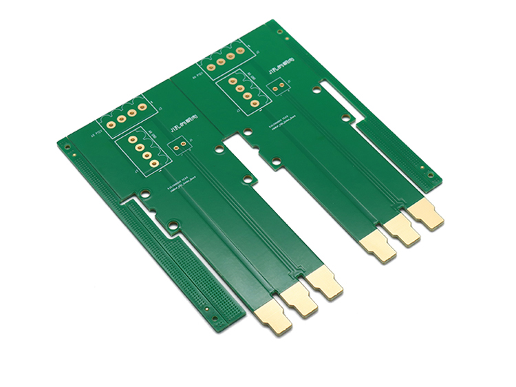
Advanced Interposer Design for AI: Organic, Glass, and Silicon Interposers in PCB
Introduction: Why Interposers Are Revolutionizing Semiconductor Packaging
The electronics industry is in the midst of a transformative era, propelled by the relentless pursuit of miniaturization, performance, and functional integration. Nowhere is this shift more evident than in semiconductor packaging—the art and science of connecting, protecting, and powering modern chips inside everything from smartphones to data center servers. Within this domain, interposers have emerged as the ultimate “bridges,” driving advanced packaging and enabling the next generation of multi-die and chiplet-based systems.
Why Interposers Matter Now
Modern hardware demands more bandwidth, faster communication, and integration of diverse semiconductor dies (logic, memory, analog, RF) into a single system—known as heterogeneous integration. This integration requires high-density, reliable interconnects that go far beyond what traditional printed circuit boards (PCBs) or classic chip packaging can deliver. Enter the interposer PCB: a specialized substrate that connects semiconductor dies with extreme precision and density.
The Intersection of Materials and Miniaturization
Materials science has played a crucial role in developing interposers capable of supporting high-density wiring (>5,000 connections per square centimeter), through-silicon vias (TSVs), advanced redistribution layers (RDLs), and even embedded passive/active circuit elements. Today’s leading-edge chip packaging often involves a carefully selected mix of:
- Silicon interposers for high-speed and high-density integration (e.g., HBM memory with GPUs).
- Glass interposers for outstanding electrical and thermal performance at scale.
- Organic interposers for cost-effective, flexible PCB integration.
The variety and performance of these interposers deeply impact the signal integrity, power delivery, and thermal management of packaged ICs.
Driving Forces in Semiconductor Interposer Adoption
The adoption and evolution of interposer design in the semiconductor industry stem from several converging trends:
- The rise of 2.5D packaging and 3D IC packaging for logic-memory integration.
- Growth in AI, machine learning, and high-performance computing, necessitating ultra-high-bandwidth connections.
- Heterogeneous integration for bringing together logic, memory, RF, analog, and photonics.
- Ever-shrinking feature sizes and the need to extend Moore’s Law through system-level innovation.
What Is an Interposer?
Interposers—sometimes called semiconductor interposers or interposer PCBs—are specially engineered substrates that physically and electrically connect multiple semiconductor dies within a single package. The fundamental role of an interposer is to serve as a bridge: it routes high-density electrical connections between dies, from dies to a package substrate, and in many designs, between the dies and the external printed circuit board (PCB).
Definition and Role in Semiconductor Packaging
At first glance, an interposer might appear similar to a very advanced multilayer PCB. However, its capabilities and design complexity go far beyond standard circuit boards. An interposer is fabricated to carry a large number of extremely fine-pitch connections—known as high-density interconnects (HDI)—and can do this in much less space than legacy PCB substrates.
The Evolution of Interposer Use in Advanced Chip Packaging
Traditional 2D and 3D Packaging vs. 2.5D Packaging
- 2D packaging: Dies are placed side-by-side on a substrate (e.g., multi-chip modules). This is limited by substrate wiring density and package size.
- 3D packaging: Dies are stacked vertically, directly bonded, typically by through-silicon vias (TSVs), for ultra-high density, but it introduces thermal management and yield issues.
- 2.5D packaging: Interposer sits between multiple dies side by side (“planar” arrangement); it enables many thousands of ultra-fine connections (microbumps) among dies, using advanced conductive layers and TSVs.
2.5D packaging has become the mainstream for high-performance, heterogeneous integration applications—graphics cards, AI inference chips, and networking ASICs—thanks largely to the enabling power of the interposer.
Where Interposers Shine
- High-bandwidth, low-latency die-to-die communication
- Efficient power and ground distribution
- Integration of different technology nodes (e.g., 7nm GPU + 28nm HBM memory)
- Simplifying test and assembly compared to monolithic 3D stacking
Types of Interposers
- Passive Interposers: Only provide wiring and mechanical support. Most organic and glass interposers fall into this category.
- Active Interposers: Feature embedded circuits, such as I/O re-timers, power management, or even logic blocks. These are usually based on silicon and are crucial for next-generation 3D IC packaging.
Anatomy of an Interposer PCB
Main Roles of the Interposer PCB
The interposer PCB performs a handful of essential functions in today’s semiconductor packages:
- Mechanical Support: Providing a platform for tiny, ultra-thin semiconductor dies (chips) to be placed in precise alignment.
- Electrical Interconnection: Routing hundreds or even thousands of signals between dies using densities far beyond standard PCBs.
- Connection to Package Substrate: Serving as a gateway to distribute connections from the small pitch (chip-level) to the larger pitch (package-level or board-level).
Key Components and Features
| Feature | Description |
|---|---|
| Pads/Microbumps | Contact points for flip-chip or hybrid bonded dies. |
| Through-Silicon Vias (TSVs) | Vertical metal vias carrying signals/power through silicon or glass interposers. |
| Redistribution Layer (RDL) | Thin copper routing layers for fanout and fine-pitch wiring. |
| C4 Bumps | Solder bumps (Controlled Collapse Chip Connection) for external connections. |
| Ball Grid Array (BGA) | For package-to-PCB connections. |
Anatomy Cross-Section Example
A cross-section of a silicon interposer typically features:
- Layers of redistribution wiring (RDL)
- TSVs embedded through the silicon
- Microbump arrays for die attachment above
- Solder balls (BGA) or C4 bumps beneath for substrate connection
Advanced Capabilities
- Impedance-controlled transmission lines for high-speed signals
- Integrated passive devices (capacitors, resistors) in or under RDLs
- Support for advanced power integrity management (multiple voltage rails, low-inductance return paths)
Material Solutions: Organic, Glass, and Silicon Interposers
Selecting the right interposer material is fundamental to balancing performance, cost, manufacturability, and reliability.
Comparative Table: Interposer Materials
| Material | Key Advantages | Limitations & Use Cases |
|---|---|---|
| Silicon | Highest wiring density; supports TSVs; excellent for high-frequency signal integrity; can be “active” | Expensive, limited substrate size, CTE mismatch risk; used in HPC, GPUs, HBM memory integration |
| Glass | High electrical insulation, very low loss tangent, large panel sizes; good for RF and optical applications | Brittle, moderate wiring density, fewer suppliers; emerging in networking, SiPhotonics |
| Organic | Cost-effective, large panels, flexible routing for lower speed signals, compatible with PCB fabs | Lower wiring density, limited for fine-pitch, signal losses at high frequency; common in consumer and automotive |
Silicon Interposers
- Best-in-class fine pitch and multi-layer RDLs
- Enables dense TSV arrays
- Used in AMD/Xilinx FPGAs, NVIDIA GPUs, chiplet-based SoCs
- May offer active interposer functions (signal conditioning, power management)
Glass Interposers
- High-frequency/radio frequency (RF) applications—glass has low dielectric loss.
- Bigger manufacturing panels than silicon, potentially lowering cost per square cm.
- Used in photonics and future high-speed data networking, owing to superior insulation.
- Example: Glass interposer for co-packaged optics in network switches.
Organic Interposers
- Based on advanced PCB materials (like RCC, ABF, or PEEK for specialty)
- Offers cost savings for less demanding signal integrity or density requirements.
- Commonly used in mainstream consumer electronics, automotive, and lower-bandwidth AI modules.
- Case Study: Adoption of PEEK-based organic interposers in harsh automotive environments for reliability at wide temperature swings.
Types of Interposers: Passive vs Active, and Package-Level Variants
Passive Interposers
A passive interposer serves purely as a routing medium; it contains no active electronic components or logic functions.
- Almost all organic and glass interposers are passive.
- Silicon interposers used in mainstream FPGAs and GPUs are often passive as well.
Benefits:
- Lower power consumption (no on-board circuits)
- Simpler manufacturing
- Less heat generation
Active Interposers
Active interposers incorporate components like I/O drivers, multiplexers, retimers, or power management circuits directly within the interposer.
- Mainly realized with silicon technology, leveraging CMOS or other semiconductor fabrication processes.
Use Cases:
- Next-gen chiplet integration, where dies use different technologies and I/O standards.
- Integration of low-latency memory buffers or switches within the interposer.
Passive vs. Active Interposers: At a Glance
| Feature | Passive Interposer | Active Interposer |
|---|---|---|
| Circuitry | No active devices | Embedded logic and/or I/O circuits |
| Material | Silicon (passive), glass, organic | Only silicon |
| Power Usage | Minimal | Higher (due to active blocks) |
| Complexity | Lower | Higher (EDA and verification needed) |
Do You Need an Organic PCB Interposer or a Package-Level Interposer?
- Use an organic PCB interposer if,
- Cost is critical,
- Density/miniaturization requirements are moderate,
- You need compatibility with standard PCB assembly lines.
- Use a package-level/silicon interposer if,
- Your design requires very high-density interconnects,
- Signal integrity and power delivery are demanding,
- You are integrating leading-edge processors/memory (e.g., HBM + ASIC).
Interposer PCB in Modern Chip Packaging: Design, Validation, and Assembly
In state-of-the-art semiconductor packaging, the interposer PCB acts not just as a conduit for signals, but also as the structural backbone of the advanced package. Its correct design and integration underpin the reliability, performance, and yield of the final electronic system, whether destined for a consumer device, networking switch, or AI accelerator.
Placement in a Package
Die placement and alignment on an interposer require nanometer-level precision. Here’s why:
- ICs are attached using microbumps or, in some high-precision processes, with hybrid bonding, enabling interconnect pitches below 40 microns.
- The interposer typically routes these connections outward and downward, fanning them out to a size compatible with a ball grid array (BGA) or large C4 solder bumps for assembly onto the main substrate or motherboard.
- State-of-the-art interposers are central to chiplet integration strategies, supporting multiple process nodes on a single substrate—e.g., combining cutting-edge logic with cost-effective analog dies or high-bandwidth memory (HBM).
Key Routing and Assembly Considerations:
- Escape and Fanout Routing: High pin-count dies require innovative fanout strategies, as traces must exit the dense microbump area without creating cross-talk or parasitic capacitance.
- Use via-in-pad techniques for minimal signal reflections.
- Ensure controlled impedance traces to meet high-speed demands.
- Table: Typical Fanout Routing Techniques
| Technique | Description | Applications |
|---|---|---|
| Via-in-pad | Via placed directly under pad | High-speed dies |
| Dogbone Fanout | Trace “necks” out before fanout | Moderate speed |
| Back-drilling | Removable stub for clean signals | 10+ Gbps signals |
How Is an Organic PCB Interposer Manufactured?
Organic interposers (and organic-rich package substrates) often use advanced HDI PCB processes like:
- Multi-step lamination,
- Laser-drilled microvias,
- Embedded or cavity copper layers,
- Application-specific surface finishes (e.g., ENIG, OSP for enhanced assembly compatibility).
EDA Toolchain Requirements
- Design Flexibility: Electronic design automation (EDA) tools must support advanced stackups, microvia placement, and simulation (signal/power/thermal).
- Verification: DRCs (design rule checks) confirm manufacturability and alignment with foundry capabilities.
How Should the Finished PCB Interposer Be Validated?
Proper validation is a must before large-scale production.
- Electrical Testing:
- Time Domain Reflectometry (TDR) for signal checks.
- Power delivery simulations for IR drop and transient behavior.
- Eye-diagram analysis for serial links to validate signal quality.
- Mechanical/Environmental Testing:
- Warpage analysis (especially for large interposers).
- High-temperature cycles and shock testing, especially for automotive-grade modules.
Silicon Interposer Technology: The Hidden Power Behind Modern AI Hardware
Perhaps the most defining trend in advanced packaging is the widespread adoption of silicon interposers—a cornerstone technology for AI, high-performance computing, and next-gen networking.
Why Use a Silicon Interposer?
Silicon interposer PCBs deliver extremely fine wiring density (often 8-12 metal layers), ultra-short die-to-die connections, and the possibility of integrating active circuit elements.
- Enable HBM (high-bandwidth memory) to be tightly coupled with compute dies.
- Provide TSV arrays for robust vertical power and ground, minimizing voltage droop and improving power integrity.
- Support high-speed signaling with minimal loss (critical for >100GBps connections).
Case Studies: Real-World Innovations
- Xilinx (AMD): The Xilinx Virtex-7 2000T FPGA was one of the world’s first commercial chips to leverage a silicon interposer, connecting four FPGA “slices” and multiple banks of HBM on a single interposer, achieving unprecedented bandwidth.
- Intel Foveros & EMIB: Intel’s Foveros integrates active interposer stacking for chiplets; EMIB (Embedded Multi-die Interconnect Bridge) uses a small silicon bridge embedded in organic substrates to provide die-to-die connections—showing hybrid solutions.
- NVIDIA + AMD: Large GPUs with integrated HBM2/3 memory stacks rely on massive silicon interposers to hit performance targets and manage heat effectively.
Interposer Design Challenges and Optimization
While interposers solve a multitude of packaging problems, their design optimization is fraught with electrical, mechanical, and manufacturing complexities.
High-Frequency Signal Transmission
- Challenge: Maintaining signal integrity at data rates of 25-112 Gbps is extremely demanding on the interposer’s traces, vias, and dielectric materials.
- Solution:
- Minimize loss using ultra-thin, low-Dk dielectrics.
- Employ stripline routing for superior noise immunity.
- Use TSVs (through-silicon vias) for short, congestion-free vertical connections.
System-Level Simulation and Warpage
- Thermal Expansion/Coefficient of Expansion (CTE) Mismatch: Silicon, glass, and organic layers expand at different rates—risking warpage, die cracking, or solder joint fractures.
- Optimization Strategies:
- Symmetrical stack-up.
- Underfill adhesives.
- Smaller die and interposer footprint.
Signal and Power Integrity
- Interposers support multiple voltage levels, each requiring separate power planes and robust decoupling.
- Simulation Tools:
- Ansys Q3D/HFSS: For parasitic extraction, EMI/EMC analysis.
- Eye-diagram simulations: Ensure channel is fit for >25Gbps PAM4/NRZ operation.
Cost, Supplier Selection, and Manufacturing Considerations
Selecting the right supplier and understanding the cost drivers for interposer PCBs are crucial for scaling advanced packages from lab to mass production.
Key Cost Drivers
- Material Type: Silicon is significantly more expensive than organic or glass, both in raw material and in processing.
- Process Complexity:
- Number of layers,
- Minimum feature sizes,
- TSV density,
- Need for active circuitry.
- Yield Rates: Large or complex interposers can suffer from low yields, impacting unit cost for high-performance IC packaging.
Supplier Considerations
- Experience:
- Familiarity with advanced packaging, especially for silicon interposers.
- Track record with your chosen materials and minimum feature sizes.
- Panel Size & Capability:
- Some suppliers can handle larger panels (key for next-gen AI and datacenter devices).
- Testing Capabilities:
- In-house electrical/mechanical validation to minimize risk.
Application-Specific Interposer Solutions
No single interposer design fits all applications—material choice, layout, and complexity depend heavily on the target device, end-market, and performance requirements. Let’s explore some key areas where tailored interposer PCB solutions have made a measurable difference in the electronics industry:
Applications in AI, High-Performance Computing, and Networking
- AI Accelerators and GPUs: Silicon interposers have become the backbone of multi-die modules that blend advanced GPU cores with stacks of High Bandwidth Memory (HBM). For instance, NVIDIA’s A100 and AMD’s MI200 feature wide, parallel channels routed through massive silicon interposers. The result: bandwidth scaling into multi-terabytes per second for neural network workloads that demand real-time access to on-package memory.
- High-End FPGAs: Devices like the Xilinx Virtex UltraScale+ use silicon interposers to connect multiple FPGA slices with HBM or custom I/O tiles, enabling large-scale logic systems and ultra-fast communication between functional blocks.
- Networking & Optical Systems: Glass interposers are increasingly being adopted where low-loss, high-frequency, and even optically-integrated channels are required. Their superior electrical performance at high speed, and the ability to embed waveguides for co-packaged optics, opens the door to switches and routers running at 800Gbps and above.
- Consumer and Automotive Applications: Cost sensitivity and moderate performance requirements make organic interposers attractive for mobile processors, ADAS (advanced driver-assistance systems), and sensor fusion hubs. These take advantage of mature PCB fabrication techniques but still deliver miniaturization and heterogeneous integration.
Specialty and Harsh Environment Solutions
Certain applications require unique combinations of reliability and electrical characteristics. For instance:
- Industrial & Harsh Environments: PEEK (polyether ether ketone) organic substrates offer exceptional chemical resistance and thermal performance, enabling interposers for aerospace, automotive under-hood, or oil-and-gas.
- Medical Devices: Glass and organic interposers are used where biocompatibility and miniaturization are essential, allowing dense sensor arrays and low-noise amplification near the sensing site.
Conclusion
The era of advanced semiconductor packaging is here—and at its heart lies the interposer PCB. As chips get smaller but more powerful, and integration of logic, memory, and analog functionality becomes routine, interposers have become the linchpin for innovation in the electronics industry.
Interposer design is no longer a niche skill; it’s fundamental to building next-generation systems for AI, networking, automotive, and consumer technologies. With the variety of available technologies—silicon, glass, or organic interposers—semiconductor companies can now optimize for bandwidth, manufacturing cost, signal integrity, or reliability, based on the end application.
As we move deeper into the age of chiplet and 2.5D/3D IC packaging, interposers will continue to grow in complexity and importance. Their ability to deliver reliable, high-density interconnections paves the way for Moore’s Law 2.0, where system-level miniaturization and heterogeneous integration are the new frontier.
Frequently Asked Questions
1. What is an interposer in semiconductor packaging?
An interposer is a micro-engineered substrate that electrically and mechanically connects multiple semiconductor dies in a single package. Interposers serve as a dense wiring “bridge” between chips—enabling high-bandwidth, low-latency data transfer and integration of heterogeneous technologies (logic, memory, RF, etc.) that would be impossible with traditional PCB routing.
2. How are silicon, glass, and organic interposers different?
- Silicon interposers offer the finest wiring density and support for through-silicon vias (TSVs), making them ideal for high-speed, high-bandwidth systems such as GPUs and AI accelerators.
- Glass interposers provide ultra-low-loss electrical properties, large panel sizes, and are particularly valuable for optical and RF applications.
- Organic interposers are cost-effective, compatible with large PCBs, and well-suited for moderate-density, mass-market devices such as consumer electronics and automotive controllers.
3. What are 2.5D and 3D packaging, and how do interposers fit in?
- 2.5D packaging refers to semiconductor dies placed side-by-side on an interposer rather than directly stacked. The interposer enables high-density connections for communication and power.
- 3D packaging stacks dies vertically—often connected by TSVs. Some advanced packages combine 2.5D (side-by-side placement on interposer) and 3D (stacked dies) techniques for maximum density and performance.
4. What is the difference between a passive and an active interposer?
- Passive interposers only route signals, power, and ground—without any active circuitry. Most organic and glass interposers, as well as many silicon types, are passive.
- Active interposers incorporate embedded circuits (such as signal buffers or power management ICs) within the interposer substrate, often using silicon CMOS technology. This allows signal conditioning and integration of extra features for demanding, heterogeneous chiplet or 3D IC packaging.
5. Why are interposers important for AI and high-performance computing?
AI, HPC, and modern GPUs require the highest bandwidth connections between compute dies and HBM memory stacks. Interposer PCBs support thousands of parallel data paths (using microbumps, TSVs, and advanced redistribution layers), making them essential for performance and energy efficiency in these applications.