PCB fabrication stands at the heart of electronics manufacturing, powering over 95% of devices worldwide. When you understand each fabrication step, you gain the skills to turn a digital printed circuit board design into a reliable product. Leading industry standards guide the process:
| Standard | Description |
|---|---|
| ISO 9001 | Quality management and performance improvement |
| ISO 14001 | Environmental management and resource efficiency |
| IATF 16949 | Automotive quality and product reliability |
You can apply the pcb fabrication process to multilayer, rigid-flex, and metal core boards.
Key Takeaways
- Understand the PCB fabrication process to transform designs into reliable products. Each step, from design to testing, is crucial for quality.
- Utilize advanced tools for design output and verification. Automated checks help identify issues early, ensuring a smoother fabrication process.
- Prioritize quality control at every stage. Following industry standards like ISO 9001 ensures your PCB meets high performance and reliability.
PCB Fabrication Process Steps

Printed Circuit Board Design
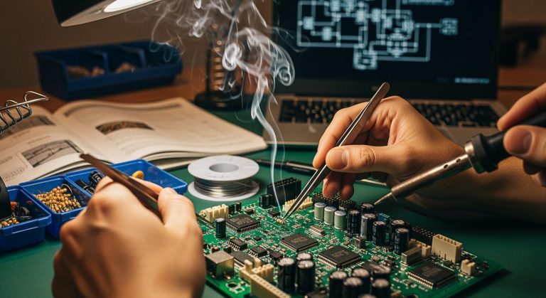
You begin the pcb fabrication process with a detailed circuit board design. This stage defines the electrical pathways, component placement, and stack-up of layers. You use advanced CAD tools to create the schematic and layout, ensuring that the design meets the requirements for multilayer, rigid-flex, or metal core boards. KING FIELD’s expertise allows you to manage complex designs with high precision, supporting fine-pitch components and high-frequency applications. By focusing on design for manufacturability, you reduce potential defects and streamline the next steps involved in pcb fabrication.
Design Output and Verification
After completing the design, you generate output files such as Gerber, drill, and netlist files. Automated verification tools play a crucial role here:
- Automated schematic integrity analysis replaces manual reviews, inspecting all nets in the design.
- Multi-dimensional verification schemes include signal integrity and power integrity analysis.
- Tools like Altium Designer® offer mixed-signal simulation for rapid validation.
- Early identification of potential problems helps enforce good pcb design practices.
You also perform testability analysis, EMI validation, and thermal assessments. These steps ensure that your printed circuit board meets industry standards and is ready for fabrication.
Inner Layer Printing
For multilayer boards, you print the inner layers first. You transfer the circuit pattern onto copper-clad laminates using photoresist and UV exposure. This process defines the intricate traces and pads that form the electrical connections within the board. KING FIELD’s intelligent compensation system accounts for material expansion and contraction, ensuring precise alignment of all layers.
Substrate Preparation
Proper substrate preparation is essential for pcb fabrication quality and reliability. You follow these steps:
- Select the appropriate substrate material for your application.
- Cut the substrate to the required dimensions.
- Clean the substrate to remove contaminants.
- Pre-treat the surface to enhance adhesion, often using a chemical primer.
The choice of substrate affects electrical performance, mechanical stability, and thermal management. High-quality substrates provide optimal insulation and minimize signal interference, ensuring your pcb performs reliably in demanding environments. Eco-friendly materials, such as biodegradable laminates, are increasingly used to reduce environmental impact.
Image Transfer
You transfer the circuit image onto the prepared substrate using one of two main methods:
- Laminate a dry film onto the copper surface.
- Expose the board to UV light through a photomask, hardening the film where light passes.
- Develop the board to remove unexposed areas, revealing the circuit pattern.
Laser Direct Imaging (LDI) offers high precision, automatic alignment, and flexibility for design changes. This technology reduces setup times and chemical use, making it ideal for complex, high-density designs.
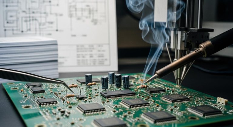
Etching Process
Etching removes unwanted copper, leaving only the desired circuit traces. You typically use chemicals like ferric chloride, cupric chloride, or persulfate-based solutions. These chemicals aggressively attack copper, so you must handle them with care to prevent environmental pollution and health risks. KING FIELD prioritizes eco-friendly alternatives and proper waste management to minimize the impact of etching on the environment. The etching process is critical for defining fine features and ensuring the integrity of all layers.
Drilling
You drill holes to create vias and mounting points. Precision is vital, especially for multilayer boards. You must align design rules with manufacturing capabilities, ensuring via diameter and spacing meet strict tolerances. Laser drills and advanced optics provide pinpoint accuracy. The table below summarizes key drilling specifications:
| Specification | Details |
|---|---|
| Drill Size | Minimum 6 mils, recommended 8-10 mils |
| Aspect Ratio | 10:1 to 20:1 |
| Via Width | Minimum 2 mils, recommended 4-6 mils |
| Via Spacing | Minimum 8 mils edge-to-edge |
Clear documentation and careful planning help prevent errors during this step.
Plating and Copper Deposition
Plating forms the conductive pathways between layers. You immerse the pcb in a copper plating bath and apply an electric current. This deposits a thin layer of copper onto the walls of drilled holes, connecting the inner and outer layers. Both electroplating and chemical plating methods are used. KING FIELD’s advanced plating techniques ensure reliable connections for multilayer, rigid-flex, and metal core boards. You may also plate edges, radii, and cutouts as needed for specialized applications.
Solder Mask Application
You apply a solder mask to protect copper traces from oxidation and prevent solder bridges during assembly. The table below highlights common solder mask types and their contributions to durability:
| Solder Mask Type | Key Properties and Contributions to Durability |
|---|---|
| Liquid Photoimageable Solder Masks | Chemical resistance, strong adhesion, thermal stability |
| Dry Film Solder Masks | Easy handling, good durability |
| Liquid Epoxy Solder Mask | Cost-effective, hardens under heat, durable |
| Top and Bottom-side Masks | Essential for protecting traces and ensuring durability |
| Chemical Resistance | Withstands processing chemicals, long-term durability |
| Adhesion | Maintains mask integrity |
| Thermal Stability | Withstands high soldering temperatures |
| Dielectric Strength | Prevents electrical failures |
| Flexibility & Hardness | Balances handling and abrasion resistance |
| Flame Retardance | Ensures safety in case of fire |
A high-quality solder mask enhances the reliability and lifespan of your printed circuit board.
Silkscreen Printing
Silkscreen printing adds important markings to the pcb surface. You use this step to label components, indicate polarity, and mark test points. The table below shows typical information included:
| Information Type | Description |
|---|---|
| Component Identifiers | Labels like “R1” for resistors or “C2” for capacitors |
| Polarity Markings | Indicators for diodes, capacitors, and other polarized components |
| Test Points | Labels for points where measurements can be taken during testing |
Clear silkscreen printing helps with assembly, inspection, and maintenance.
Surface Finish
You apply a surface finish to exposed copper areas to improve solderability and protect against oxidation. Common finishes include:
| Surface Finish Type | Advantages | Disadvantages |
|---|---|---|
| HASL | Cost-effective, good shelf life | Not ideal for fine pitch components |
| Lead Free HASL | RoHS compliant | Similar to traditional HASL |
| ENIG | Excellent flatness, corrosion resistance | More expensive, prone to defects |
| OSP | Environmentally friendly, cost-effective | Limited shelf life, less durable |
| Immersion Tin/Silver | Smooth surfaces, good for high-density boards | Can tarnish, requires careful handling |
The right finish ensures reliable solder joints and long-term performance.
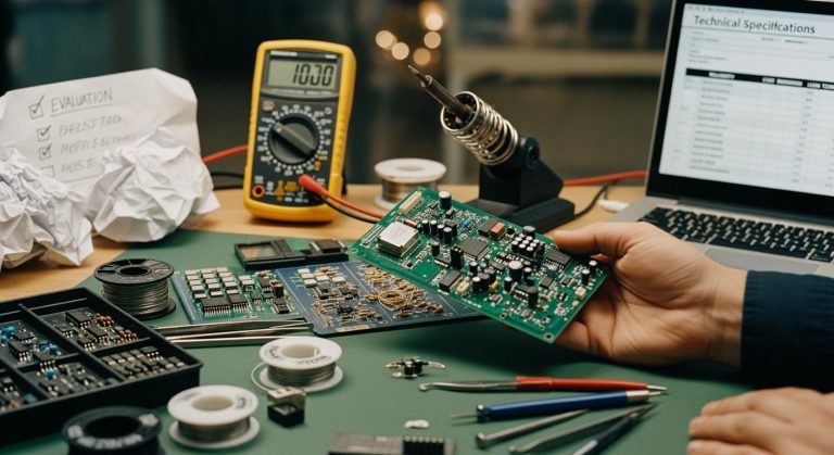
Electrical Testing
You perform electrical testing to verify the functionality and reliability of the pcb. Common tests include:
- Vibration and thermal shock tests
- Burn-in (HALT/HASS) and environmental exposure tests
- Electrical stress and UL safety tests
These tests confirm that your printed circuit board meets industry standards and will perform reliably in its intended application.
Board Cutting and Profiling
In the final step, you separate individual boards from the production panel. You can use routing, scoring, or v-groove methods:
- Profiling defines the shape and size of each pcb.
- Routing creates small tabs for easy separation.
- Scoring and v-groove methods cut channels for simple break-off.
This step ensures each board matches the design specifications and is ready for assembly.
Tip: By following each step in the pcb fabrication process and working with a manufacturer like KING FIELD, you ensure high quality, reliability, and environmental responsibility in every printed circuit board you produce.
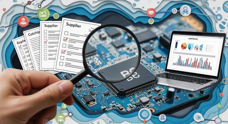
Quality Control in PCB Fabrication

Inspection and Testing
You must ensure quality at every stage of the pcb fabrication process. KING FIELD follows strict international standards, including ISO 9001 and IATF 16949, to maintain high-quality production. These standards focus on defect prevention, risk management, and supplier reliability. You integrate customer-specific requirements into the quality management system, which helps you meet unique client needs.
You use a range of inspection and testing methods to verify the integrity of each pcb. Common techniques include:
- Manual visual inspection for surface defects and copper trace alignment
- Automated Optical Inspection (AOI) for detecting solder mask and silkscreen issues
- In-circuit testing and flying probe tests for electrical continuity
- X-ray inspection for multilayer boards to check for hidden copper connections
- Functional tests to confirm that the printed circuit board performs as designed
You also perform continuity tests, hi-pot tests, and resistivity of solvent extract (ROSE) tests. These steps help you catch any issues before the final quality check. You repeat these inspections after final etching and before the board leaves the facility.
Reliability Assurance
You must guarantee that every pcb will perform reliably in its intended environment. KING FIELD uses advanced reliability testing for multilayer, rigid-flex, and metal core boards. You conduct ESD and EMP testing to assess resistance to electrostatic discharge and electromagnetic pulses. Moisture resistance testing helps you understand how much water vapor the board can withstand without copper corrosion or damage.
You simulate real-world conditions with vibration and low-pressure testing. Thermal cycling tests measure how well the copper layers handle repeated heating and cooling. These tests ensure that the fabrication process produces boards that meet strict reliability standards. You complete a final quality check after all reliability tests and final etching to confirm that each pcb is ready for use.
Note: By following these quality steps, you ensure that every pcb meets the highest standards for performance and durability.
You gain a clear understanding of the pcb fabrication process by following each step, from design to final inspection. Quality control and adherence to industry standards ensure your printed circuit board meets strict requirements. Choosing KING FIELD gives you access to advanced customization, reliable fabrication, and strong customer support.
| Advantage | Description |
|---|---|
| Customization Capabilities | Wide range of options for your pcb design needs |
| High-Quality Standards | Consistent quality and reliable production |
| Strong Customer Service | Effective support for your project requirements |
FAQ
What is the difference between PCB fabrication and the pcb assembly process?
You create the board during PCB fabrication. The pcb assembly process adds components to the finished board, turning your circuit board design into a working device.
Why is chemical etching important in PCB manufacturing?
You use chemical etching to remove unwanted copper. This step defines the circuit paths and ensures accuracy before the final quality check.
When do you perform the final quality check in PCB production?
You complete the final quality check after final etching and all inspections. This step ensures your board meets design and reliability standards.