Top 10 Essential Tools for ASSY PCB in 2025

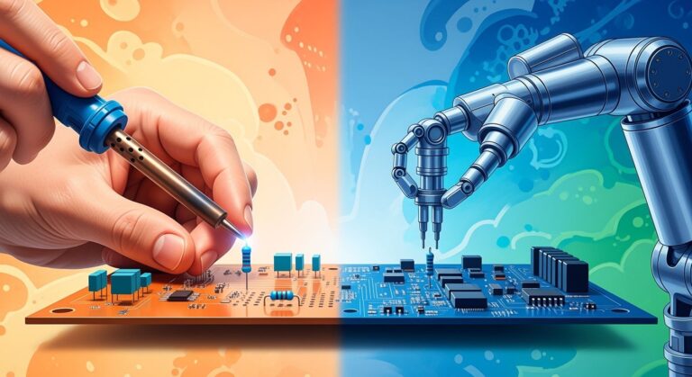
The world of ASSY PCB manufacturing is evolving rapidly, and staying ahead requires adopting cutting-edge tools. Advanced equipment transforms the way you approach PCB assembly, boosting efficiency and reducing errors. For instance, intelligent mounters have increased per capita output in SMT workshops by nearly 60%, while defective rates have dropped by over 30%. These innovations not only streamline production but also ensure the reliability of electronic devices. As electronic devices grow more complex, precision becomes paramount. Modern tools empower you to meet these demands with unmatched accuracy and consistency in ASSY PCB processes.
Key Takeaways
- Automated pick-and-place machines work fast and accurately. They can place over 50,000 parts each hour and make fewer mistakes.
- Modern solder paste printers apply paste neatly. This reduces problems and makes solder joints stronger.
- Advanced reflow ovens control heat carefully. They stop overheating and spread heat evenly for better soldering.
- Automated optical inspection (AOI) systems find mistakes early. This improves product quality and lowers costs by checking efficiently.
- Smart storage systems help manage inventory better. They make sure parts are ready on time and avoid extra costs from too much stock.
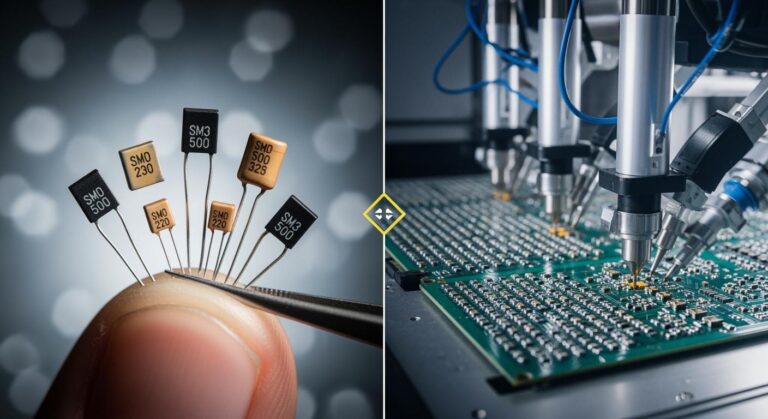
Automated Pick-and-Place Machines
Speed and Accuracy in Component Placement
Automated pick-and-place machines revolutionize PCB assembly by delivering unmatched speed and precision. These machines can place tens of thousands of components per hour, with top-tier models exceeding 50,000 components per hour (CPH). Their placement accuracy, measured at ±0.05 mm, ensures that even the smallest components are positioned correctly.
- Key Benefits of Speed and Accuracy:
- High-speed placement reduces production cycle times, enabling faster delivery of finished products.
- Precision minimizes errors, preventing costly malfunctions in electronic devices.
- Real-time monitoring systems detect anomalies instantly, reducing waste and improving overall efficiency.
These machines excel in handling complex designs, where component density and placement accuracy are critical. By automating the placement process, you eliminate manual errors and achieve consistent results across large production runs.
Automation for High-Volume Production
For high-volume PCB manufacturing, automation is indispensable. Modern pick-and-place systems integrate advanced features that streamline production while maintaining quality. Metrics such as precision, efficiency, and quality control have seen significant improvements with these systems:
| Metric | Description |
|---|---|
| Precision | Ensures that even minor errors are detected, preventing malfunctions in electronic devices. |
| Real-time monitoring | Allows for immediate detection of anomalies, reducing defects and waste during production. |
| Enhanced efficiency | Increases production output and reduces cycle times, leading to faster component placement. |
| Quality control improvement | Advanced inspection systems enable quick correction of defects, enhancing overall product quality. |
Automation also supports scalability. Whether you’re producing hundreds or thousands of units, these machines adapt to your needs without compromising performance. By investing in automated pick-and-place systems, you position your assembly line to meet the growing demands of the PCB industry in 2025.
Solder Paste Printers
Precision in Solder Paste Application
Achieving precision in solder paste application is critical for ensuring reliable PCB assembly. Modern solder paste printers deliver exceptional accuracy by controlling key parameters such as volume, alignment, and coverage. These metrics directly impact the quality of solder joints and the overall functionality of the board.
- Key Precision Metrics:
- Solder Paste Volume: Maintains a tolerance of ±30% to ensure proper joint formation.
- Area Coverage: Targets 80-100% coverage to prevent poor connections or bridging.
- Height and Shape: Ensures uniformity with a height tolerance of ±50%.
- Alignment (X, Y, and θ): Keeps alignment within ±50% of pad width or 50 μm for accurate placement.
- Consistency Across the Board: Identifies systematic issues by analyzing variations.
Modern printers utilize advanced technologies like 3D solder paste inspection (SPI) to monitor these parameters in real time. This ensures that every deposit meets the required specifications, reducing the risk of defects during subsequent assembly stages.
Reducing Defects with Modern Printers
Innovations in solder paste printers have significantly reduced defects in PCB assembly. These machines now incorporate features that optimize paste deposition and minimize common issues like bridging, voiding, and misalignment. The choice of solder paste also plays a crucial role in defect prevention.
| Characteristic | Details |
|---|---|
| Alloy Choice | Low-temp solders for heat-sensitive parts; high-temp for harsh environments. |
| Powder Type | Transition to finer powders (Type 4-6) reduces bridging and improves fill. |
| Powder Shape & Oxide Level | Spherical powder with low oxide content ensures consistent quality. |
| Flux Chemistry | No-Clean and Water-Soluble fluxes offer tailored cleaning and activity options. |
Modern printers also integrate AI-driven inspection systems to detect and correct errors during the printing process. These systems analyze solder paste deposits for uniformity and alignment, ensuring consistent results across the board. By adopting these advanced tools, you can significantly enhance the reliability and performance of your PCB assemblies.
Reflow Ovens
Advanced Temperature Control for Soldering
Reflow ovens play a critical role in ensuring high-quality soldering during PCB assembly. Advanced temperature control systems in modern ovens allow you to achieve precise thermal profiles tailored to the specific requirements of your components and solder paste. These profiles ensure that each stage—preheat, soak, reflow, and cooling—occurs at the optimal temperature and duration.
- Key Benefits of Advanced Temperature Control:
- Prevents overheating, which can damage sensitive components.
- Ensures uniform heat distribution across the PCB, reducing cold solder joints.
- Supports lead-free soldering, which requires higher and more precise temperatures.
Modern reflow ovens often feature multi-zone heating systems, enabling you to fine-tune temperatures for different sections of the board. Some models also incorporate real-time monitoring and feedback mechanisms, allowing you to adjust parameters on the fly. This level of control minimizes defects and ensures consistent results, even for complex multilayer boards.
Pro Tip: Use profiling tools to measure and optimize the thermal curve for each PCB design. This ensures compliance with industry standards and enhances product reliability.
Energy Efficiency in Reflow Ovens
Energy efficiency has become a top priority in PCB manufacturing, and reflow ovens have evolved to meet this demand. Modern ovens incorporate energy-saving technologies that reduce power consumption without compromising performance. Features like insulated chambers, optimized airflow systems, and intelligent power management help you lower operational costs while maintaining high throughput.
| Feature | Benefit |
|---|---|
| Insulated Chambers | Minimizes heat loss, reducing energy waste. |
| Optimized Airflow Systems | Ensures even heat distribution with less energy usage. |
| Intelligent Power Modes | Automatically adjusts energy consumption based on production requirements. |
Energy-efficient ovens not only reduce costs but also align with sustainability goals. Many manufacturers now offer models with eco-friendly certifications, ensuring compliance with environmental regulations. By investing in these advanced systems, you can enhance your production line’s efficiency while reducing its carbon footprint.
Note: Regular maintenance, such as cleaning filters and calibrating sensors, further improves energy efficiency and extends the lifespan of your reflow oven.
AOI (Automated Optical Inspection) Systems
Early Defect Detection in PCB Assembly
Automated optical inspection (AOI) systems are indispensable for identifying defects early in the PCB assembly process. These systems use predefined tolerance values to ensure compliance with quality standards, allowing you to detect issues before they escalate into costly failures. By leveraging advanced machine vision technology, AOI systems inspect thousands of components per hour, far surpassing the capabilities of manual inspection.
- Why AOI Systems Excel in Early Detection:
- Achieve an accuracy rate of 98-99%, compared to 85-90% for manual methods.
- Inspect over 5,000 components per hour, while manual inspection handles only 500-800.
- Reduce false calls and improve the detection of genuine defects, enhancing operational efficiency.
Early defect detection not only improves product quality but also reduces operational costs. By catching errors at the initial stages, you minimize rework and scrap, ensuring a smoother production flow. The integration of AI further enhances these systems, enabling them to adapt to complex designs and evolving industry standards.
Tip: Regularly update the tolerance values in your AOI system to align with the latest PCB designs and manufacturing requirements. This ensures consistent performance and compliance with quality benchmarks.
AI-Powered Quality Control
AI-powered quality control transforms the way you approach PCB assembly. These systems use predictive models to analyze inspection data, identifying patterns that signal potential defects. With accuracy rates reaching up to 95%, AI-driven AOI systems significantly outperform traditional methods.
| Performance Metric | Description |
|---|---|
| Accuracy Rate | AI-based defect detection achieves up to 95% accuracy. |
| Failure Rate Reduction | Predictive AI models reduce PCB failure rates by 35%. |
The ability to predict and prevent defects before they occur is a game-changer for PCB manufacturing. AI algorithms continuously learn from inspection data, refining their detection capabilities over time. This reduces false positives and ensures that only genuine issues are flagged for review.
By adopting AI-powered AOI systems, you gain a competitive edge in the market. These tools not only enhance quality control but also streamline your production process, allowing you to meet the growing demand for high-performance electronic devices.
Pro Tip: Use AI-driven analytics to identify recurring defects and optimize your assembly line. This proactive approach improves efficiency and reduces downtime.
X-Ray Inspection Systems

Ensuring Solder Joint Integrity
X-ray inspection systems are indispensable for verifying solder joint integrity in PCB assembly. These systems allow you to examine solder joints beneath components like BGAs (Ball Grid Arrays) and QFNs (Quad Flat No-leads), where traditional optical methods fall short. By using non-destructive imaging, you can identify hidden defects such as voids, insufficient solder, or bridging that compromise the reliability of your boards.
Modern X-ray systems provide high-resolution imaging, enabling you to detect even the smallest anomalies. Advanced models also feature 3D computed tomography (CT), which reconstructs cross-sectional views of solder joints. This capability ensures a thorough analysis of joint quality, helping you meet stringent industry standards.
Tip: Regularly inspect solder joints during production to catch defects early. This minimizes rework and ensures consistent product quality.
Essential for Multilayer and High-Density Boards
As PCB designs grow more complex, X-ray inspection becomes essential for multilayer and high-density boards. These boards often feature stacked vias, microvias, and densely packed components, making surface-level inspections inadequate. X-ray systems excel in evaluating internal structures, ensuring the integrity of connections that are otherwise inaccessible.
Here’s how X-ray inspection addresses the challenges of multilayer and high-density PCBs:
| Evidence Type | Description |
|---|---|
| Internal Defect Detection | Identifies hidden defects in multilayer boards, such as delamination or cracks. |
| Evaluation of Internal Vias | Assesses the quality of stacked or filled microvias for reliable connections. |
| Detection of Voids and Misalignment | Reveals issues like voids, incomplete fills, or misaligned layers. |
These capabilities make X-ray systems a critical tool for ensuring the performance and durability of advanced PCBs. By adopting this technology, you can maintain high production standards and meet the demands of cutting-edge electronic designs.
Pro Tip: Use X-ray inspection data to refine your manufacturing processes. This proactive approach reduces defect rates and enhances overall efficiency.
PCB Design Software with DFM Integration
Streamlining Design-to-Manufacturing Processes
PCB design software with Design for Manufacturing (DFM) integration bridges the gap between design and production. By embedding manufacturing constraints directly into the design process, you can avoid costly errors and ensure a seamless transition from concept to fabrication. This approach eliminates the need for multiple redesigns, saving both time and resources.
Modern tools equipped with DFM features allow you to identify potential manufacturing issues early. For example, they highlight problems like insufficient trace widths or improper spacing before the design reaches the production stage. This proactive approach reduces forecasting errors by up to 65% and improves design verification processes. The result? Fewer redesign iterations and significant cost savings.
| Evidence Type | Statistic/Claim |
|---|---|
| Reduction in forecasting errors | 30–65% |
| Improvement in design verification | Early identification of potential issues |
| Reduction in redesign iterations | Cost savings and efficiency |
By streamlining the design-to-manufacturing workflow, these tools empower you to deliver high-quality PCBs faster and more efficiently. This capability is especially critical in 2025, where rapid innovation demands shorter production cycles.
Key Features for 2025 PCB Design Tools
The best PCB design tools in 2025 will prioritize DFM considerations to enhance production efficiency. These tools will guide you in designing boards with proper trace widths, spacing, and other manufacturing-friendly features. Advanced software will also integrate quality control mechanisms, such as automated inspection systems, to monitor every fabrication step and ensure reliability.
| Key Performance Indicator | Description |
|---|---|
| DFM Considerations | Designing boards with production efficiency in mind, including proper trace widths and spacing. |
| Manufacturing Quality Control | Monitoring every fabrication step using inspection systems like AOI and conducting reliability tests. |
| Collaboration with Experienced Manufacturers | Working with specialized manufacturers to refine designs and optimize production processes. |
Collaboration will also play a pivotal role. By working closely with experienced manufacturers, you can refine your designs and optimize production processes. These features ensure that your PCBs meet both functional and manufacturing requirements, giving you a competitive edge in the market.
Pro Tip: Regularly update your design software to leverage the latest DFM features. This ensures compliance with evolving industry standards and enhances your production efficiency.
Stencil Printers
Achieving Precise Solder Paste Deposition
Stencil printers play a pivotal role in surface-mount technology (SMT), ensuring accurate solder paste application on bare PCBs. These tools enable precise deposition by guiding the paste through finely crafted apertures, aligning perfectly with the pads on the board. This process is critical for maintaining the integrity of solder joints and ensuring the functionality of the final product.
- Key Benefits of Stencil Printing:
- Stencils ensure precise material placement, reducing the risk of bridging or insufficient paste.
- Smooth paste transfer through the stencil enhances print quality and consistency.
- Accurate deposition minimizes defects during reflow soldering, improving overall assembly reliability.
The design and quality of the stencil directly impact the precision of solder paste application. Advanced stencil printers utilize optimized screen-printing techniques to achieve uniform paste distribution across all pads. This level of accuracy is essential for high-density boards, where even minor inconsistencies can lead to significant performance issues.
Tip: Regularly inspect and maintain your stencils to prevent wear and ensure consistent paste deposition. Proper care extends their lifespan and enhances production efficiency.
Innovations in Stencil Technology
Modern stencil technology has evolved to meet the demands of increasingly complex PCB designs. Innovations in manufacturing methods have significantly improved precision, enabling you to achieve tighter tolerances and smoother paste release. Below is a comparison of key manufacturing methods used in stencil production:
| Manufacturing Method | Precision Achieved (mil) | Standard Deviation (mil) | Pros/Cons Summary |
|---|---|---|---|
| Photo-Chemical Etching | 2.36 (target 2.0) | 0.11–0.19 | Cost-effective but less precise; deeper step-downs can affect paste volume control. |
| Laser Welded Technology | 2.08 (target 2.0) | 0.15–0.19 | High precision; suitable for complex designs but higher cost and longer production time. |
| Micro-Machining Technology | 2.01 (target 2.0) | 0.15–0.19 | Excellent accuracy; smooth surface finish enhances paste release but limited scalability due to costs. |
These advancements allow stencil printers to handle intricate designs with ease, ensuring consistent results even for high-density and multilayer boards. The integration of micro-machining technology, for instance, delivers exceptional accuracy and smooth surface finishes, which are vital for achieving optimal paste release.
Pro Tip: Choose the manufacturing method that aligns with your production needs. For high-volume runs, prioritize scalability and cost-effectiveness, while for complex designs, focus on precision and quality.
Innovative stencil designs also incorporate features like nano-coatings to reduce paste adhesion and improve transfer efficiency. By leveraging these advancements, you can enhance the reliability of your PCB assemblies and meet the stringent demands of modern electronics manufacturing.
Component Storage and Handling Systems
Preventing Damage and Ensuring Traceability
Proper storage and handling systems are critical for maintaining the integrity of sensitive electronic components. Mishandling or improper storage can lead to physical damage, contamination, or electrostatic discharge (ESD), all of which compromise the functionality of your PCBs. Modern storage solutions mitigate these risks by incorporating advanced technologies and preventive measures.
Preventive maintenance schedules, based on manufacturer recommendations, play a vital role in avoiding unexpected breakdowns. Predictive maintenance techniques, such as vibration analysis, further enhance reliability by identifying potential issues before they escalate. Additionally, implementing a computerized maintenance management system (CMMS) ensures a structured approach to planned maintenance, reducing emergency repairs. IoT-enabled real-time monitoring provides early warnings about developing problems, allowing you to address them proactively.
| Evidence Type | Description |
|---|---|
| Preventive Maintenance Schedules | Created based on manufacturer recommendations, helping to prevent breakdowns before they occur. |
| Predictive Maintenance Techniques | Techniques like vibration analysis help determine optimal maintenance timing, reducing failures. |
| CMMS Implementation | Companies see reductions in emergency repairs and increases in planned maintenance activities. |
| IoT Real-time Monitoring | Provides early warnings about developing issues, allowing for timely inspections before failures. |
By adopting these strategies, you not only protect your components but also ensure traceability. Advanced systems track each component’s journey through the supply chain, providing detailed records for compliance and quality assurance.
Smart Storage for Inventory Management
Efficient inventory management is essential for optimizing production workflows and minimizing costs. Smart storage systems leverage technologies like AI and IoT to streamline inventory processes, ensuring you always have the right components at the right time. These systems provide real-time tracking, automated reordering, and enhanced visibility across multiple locations.
AI-driven demand forecasting analyzes historical data and market trends to predict future needs accurately. This reduces overstocking and stockouts, improving cash flow and operational efficiency. Real-time inventory tracking ensures instant updates on stock levels, enabling proactive replenishment and accurate order fulfillment. Automated reordering systems dynamically set stock thresholds, triggering orders when levels fall below the minimum requirement.
| Performance Metric | Description | Benefits |
|---|---|---|
| Accurate Demand Forecasting | Utilizes AI to analyze various data points for predicting future demand. | Reduces overstock, fewer stockouts, and improves cash flow. |
| Real-Time Inventory Tracking and Visibility | Provides instant updates on inventory levels across locations. | Enhances visibility, proactive replenishment, and fulfillment accuracy. |
| Automated Reordering and Stock Allocation | Dynamically sets stock thresholds and triggers orders automatically. | Minimizes manual errors and maintains optimal stock levels. |
| Cost Savings and Efficiency Gains | Achieves reductions in holding costs and labor through automation. | Lowers storage fees and reduces waste from unsold goods. |
| Supplier and Supply Chain Optimization | Analyzes supplier performance to improve supplier selection and contract negotiations. | Mitigates supply chain disruptions and enhances supplier relationships. |
Smart storage systems not only improve efficiency but also reduce costs associated with manual errors and excess inventory. By integrating these solutions into your assembly line, you can achieve a seamless production process while maintaining high standards of quality and reliability.
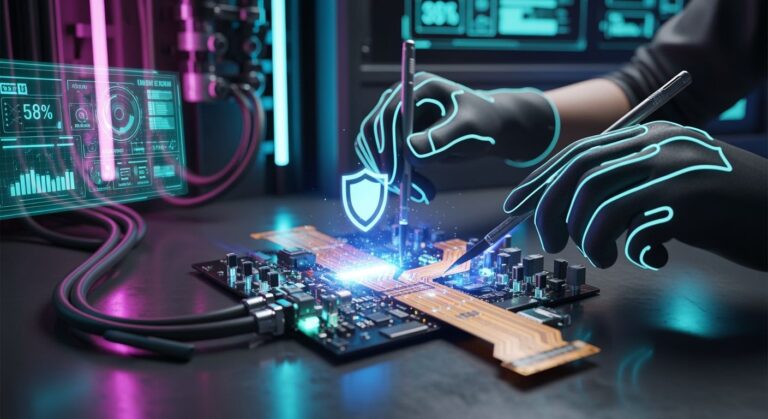
ESD Protection Tools
Safeguarding Sensitive Components
Electrostatic discharge (ESD) poses a significant threat to the integrity of electronic components during assembly. Even a minor static charge can damage sensitive parts, leading to malfunctions or complete failure of the printed circuit board. To mitigate these risks, you must implement robust ESD protection measures in your workspace.
ESD workbenches are essential for creating a controlled environment that minimizes static buildup. These workbenches feature high-resistance dissipative surfaces that safely dissipate static electricity, protecting smd components and enhancing workflow efficiency. Grounding all elements of the workspace to a common electrical ground point further prevents rapid discharges that could harm circuitry. By integrating these measures, you ensure the reliability of your soldering applications and reduce production inefficiencies.
Additionally, using ESD-safe soldering tools, such as a soldering station with built-in grounding, is critical. These tools prevent static buildup during soldering applications, safeguarding the delicate components on your printed circuit board. Incorporating ESD-safe soldering flux also helps maintain the integrity of solder joints, ensuring long-term performance.
Tip: Regularly test your ESD protection setup to ensure it meets industry standards. This proactive approach minimizes risks and enhances the durability of your printed circuit boards.
Must-Have Tools for Modern Assembly Lines
Equipping your assembly line with the right ESD protection tools is vital for maintaining quality and efficiency. Start with an ESD-safe soldering station. These stations feature grounded soldering irons that prevent static discharge during soldering applications. Look for models with adjustable temperature controls and interchangeable soldering tips to handle various tasks with precision.
Investing in ESD-safe storage solutions is equally important. Anti-static bins and component trays protect smd components from electrostatic damage during handling and storage. Pair these with ESD-safe wrist straps and mats to create a comprehensive protection system. These tools ensure that every stage of the assembly process, from storage to soldering, adheres to strict ESD safety standards.
For high-volume production, consider automated ESD monitoring systems. These systems provide real-time feedback on static levels in your workspace, allowing you to address potential issues before they escalate. By integrating these advanced tools, you not only safeguard your components but also position your assembly line to meet the demands of the competitive printed circuit board market.
Pro Tip: Train your team on proper ESD handling techniques. Even the best tools cannot compensate for improper handling practices.
Soldering Stations with IoT Capabilities
Real-Time Monitoring for Precision Soldering
IoT-enabled soldering stations are transforming the way you approach precision soldering. These advanced systems provide real-time monitoring, allowing you to track critical parameters such as temperature, power usage, and soldering iron performance. This ensures consistent results, even for the most intricate printed circuit board designs. By leveraging IoT technology, you can identify and address potential issues before they impact production quality.
The benefits of real-time monitoring extend beyond quality control. IoT-enabled systems significantly improve operational efficiency and asset utilization. The following table highlights key metrics and their improvement percentages:
| Metric | Improvement Percentage |
|---|---|
| Increase in Uptime | 41% |
| Increase in Asset Utilization | 35% |
| Efficiency Improvement | 16% |
These improvements translate to fewer interruptions, better resource management, and higher throughput. With real-time data at your fingertips, you can make informed decisions that enhance the reliability of your soldering station and the overall quality of your printed circuit boards.
Tip: Regularly analyze the data from your IoT-enabled soldering station to identify trends and optimize your soldering processes.
The Future of Soldering Stations in PCB Assembly
The future of soldering stations lies in their ability to adapt to the evolving demands of the printed circuit board market. Digital soldering stations equipped with IoT capabilities are leading this transformation. These stations offer features like automated temperature adjustments, predictive maintenance alerts, and integration with other smart manufacturing tools. This ensures seamless operation and reduces downtime.
As the printed circuit board market grows more competitive, adopting these advanced soldering stations becomes essential. They not only improve the precision of your soldering iron but also enhance the scalability of your production line. For instance, automated calibration ensures that every soldering iron operates at peak efficiency, reducing the risk of defects in high-volume production.
The integration of AI and machine learning into digital soldering stations will further revolutionize the industry. These technologies will enable predictive analytics, allowing you to anticipate maintenance needs and optimize workflows. By investing in these innovations, you position your assembly line to meet the demands of the future printed circuit board market.
Pro Tip: Stay ahead by upgrading to IoT-enabled soldering stations that offer AI integration. This ensures your production line remains competitive and efficient.
The global printed circuit board market continues to evolve, driven by the increasing complexity of electronic devices and the demand for higher production efficiency. Advanced tools for ASSY PCB assembly play a pivotal role in meeting these challenges. They enhance precision, reduce defects, and streamline workflows, ensuring that manufacturers stay competitive in the growing printed circuit board market.
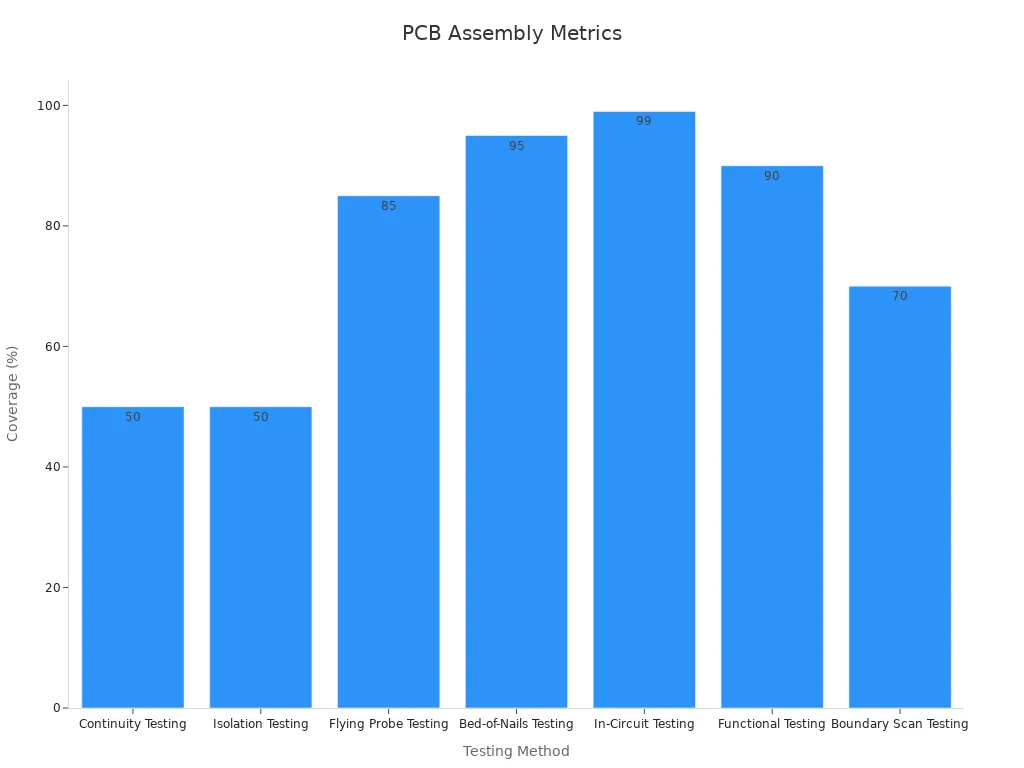
Modern testing methods, such as in-circuit testing, achieve up to 99% fault detection accuracy, significantly improving product reliability. The chart below highlights the test coverage of various methods, showcasing the importance of adopting advanced tools in PCB assembly.
As the Asia Pacific printed circuit board market leads global market growth, adopting these tools becomes essential for capturing market share. By leveraging innovations in soldering, inspection, and storage, you can optimize production processes and meet the demands of the expanding market size. Staying ahead in the competitive landscape requires embracing these advancements to deliver high-quality PCBs that power the next generation of electronic devices.
FAQ
What is the most critical tool for ASSY PCB in 2025?
Each tool plays a vital role, but automated pick-and-place machines stand out for their speed and precision. These machines streamline high-volume production and ensure accurate component placement, making them indispensable for modern PCB assembly.
How does AI improve PCB assembly processes?
AI enhances defect detection and quality control. Tools like AOI systems use AI to identify patterns, predict potential issues, and reduce false positives. This ensures higher accuracy and efficiency in your assembly line.
Why is ESD protection essential in PCB assembly?
Electrostatic discharge can damage sensitive components, leading to malfunctions. ESD-safe tools and workspaces prevent static buildup, safeguarding your PCBs and ensuring reliable performance in electronic devices.
Are IoT-enabled soldering stations worth the investment?
Yes, IoT-enabled soldering stations provide real-time monitoring, predictive maintenance, and automated adjustments. These features improve precision, reduce downtime, and enhance overall production efficiency, making them a valuable addition to your assembly line.
How do X-ray inspection systems benefit multilayer PCBs?
X-ray systems detect hidden defects like voids, misalignments, and delamination in multilayer boards. They ensure solder joint integrity and internal connection reliability, which are critical for complex, high-density designs.