Pros and Cons of Multilayer PCB Assembly in 2025
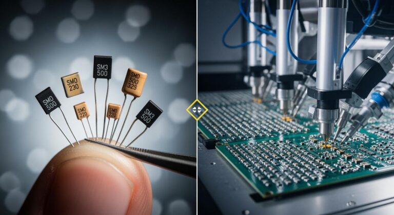
The assembly of multilayer printed circuit boards (PCBs) has transformed the electronics industry by enabling compact designs and advanced functionalities. You encounter these PCBs in devices ranging from smartphones to automotive systems. Their layered structure allows for increased complexity while maintaining a smaller footprint. However, this innovation comes with both advantages and disadvantages. While multilayer PCB assembly offers enhanced performance and reliability, it also demands higher manufacturing costs and intricate designs associated with multi-layer PCB fabrication.
In 2025, the significance of multilayer PCB assembly has reached new heights. The market continues to expand, fueled by the demand for miniaturized and efficient electronics. Forecasts indicate substantial growth, driven by a compound annual growth rate (CAGR) of X%. Industries like telecommunications and consumer electronics increasingly rely on these PCBs to integrate more functionalities into devices. As the Internet of Things (IoT) proliferates, you’ll find multilayer PCBs indispensable for meeting modern design challenges, showcasing the importance of both multilayer PCB assembly and multi-layer PCB fabrication in the evolving tech landscape.
Key Takeaways
- Multilayer PCBs help make smaller devices with more features.
- They improve how signals work and lower interference, great for fast tech.
- These PCBs cost more to make and are harder to design.
- Good heat control is needed to stop overheating in powerful devices.
- Using green materials and methods can make PCBs better for the planet.
Understanding Multilayer PCB Assembly
What Is a Multilayer PCB?
A multilayer PCB is a type of printed circuit board that consists of three or more conductive layers stacked together. These layers are separated by insulating materials and interconnected through vias, enabling complex circuit designs in a compact form. Unlike single-layer or double-layer boards, multilayer PCBs allow for higher functionality and performance by accommodating more components and connections within a smaller footprint.
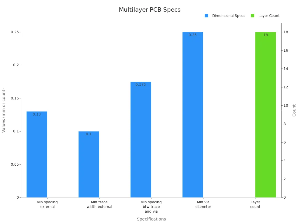
The technical specifications of multilayer PCBs highlight their advanced capabilities. For example, modern multilayer boards can feature up to 18 layers, with dimensions of 133.2mm x 196.5mm and an aspect ratio of 11:1. They also support high-frequency materials, resin-plugged vias, and efficient thermal dissipation. These features make them ideal for applications requiring high-speed signal transmission and reliability.
| Specification | Value |
|---|---|
| Layer count | 18 layers |
| PCB dimension | 133.2mm x 196.5mm |
| Aspect ratio | 11:1 |
| Minimum spacing (external) | 0.13mm |
| Minimum trace width (external) | 0.10mm |
| Minimum spacing between trace and via | 0.175mm |
| Minimum via diameter | 0.25mm |
| Substrate material properties | High-frequency material, back drilling, high aspect ratio, resin-plugged via, high thermal dissipation via |
Why Multilayer PCBs Are Essential in 2025
In 2025, the demand for multilayer PCBs continues to grow due to their critical role in modern electronics. Industries such as telecommunications, automotive, and consumer electronics rely heavily on these boards to meet the increasing need for compact and high-performance devices. Smartphones, advanced networking equipment, and automotive electronic control units (ECUs) are just a few examples of applications where multilayer PCBs excel.
The market for multilayer PCBs reflects this growing importance. In 2023, the global market was valued at $71 billion and is projected to reach $116.1 billion by 2032, with a compound annual growth rate (CAGR) of 5.5% from 2024 to 2032. This growth is driven by the technical benefits of multilayer PCBs, including their small size, lightweight design, and enhanced durability. Additionally, their ability to integrate multiple layers into a single board allows for high capacity and speed, making them indispensable for cutting-edge technologies.
The advanced materials used in multilayer PCBs further enhance their performance. Substrates with low dielectric constants (Dk) and low dielectric loss (Df) ensure efficient signal transmission and minimal signal loss. These properties, combined with low hygroscopicity and smooth copper foil, make multilayer PCBs a cornerstone of innovation in 2025.
Advantages of Multilayer PCB Assembly
Compact Size and Lightweight Design
One of the most notable advantages of multilayer PCB assembly is its ability to deliver compact and lightweight designs. By stacking multiple layers of conductive material, you can achieve higher functionality without increasing the physical size of the board. This feature is especially critical in 2025, where the demand for smaller, more portable devices continues to grow.
Multilayer PCBs allow you to integrate complex circuits into a single board, eliminating the need for multiple interconnected single-layer or double-layer PCBs. This consolidation reduces the overall weight and size of the final product. For instance, smartphones and wearable devices rely heavily on this technology to maintain their sleek and lightweight designs while offering advanced features.
The compact nature of multilayer PCBs also contributes to cost savings in terms of material usage and assembly. By minimizing the need for additional components and connectors, you can streamline the manufacturing process and reduce the risk of assembly errors. This efficiency makes multilayer PCB assembly a preferred choice for industries prioritizing miniaturization and portability.
Enhanced Performance and Functionality
Multilayer PCBs excel in delivering superior performance and functionality compared to their single-layer and double-layer counterparts. The ability to incorporate multiple layers enables you to design circuits with higher density and complexity, supporting advanced technologies like 5G, IoT, and AI-driven systems.
A key advantage of multilayer PCBs is their enhanced signal integrity. By dedicating specific layers to power planes and ground planes, you can minimize electromagnetic interference (EMI) and ensure stable signal transmission. This feature is particularly beneficial for high-frequency applications, where signal loss and crosstalk can significantly impact performance. According to market data, multilayer PCBs dominate the market share in 2023, reflecting their superior capabilities in addressing modern technological demands.
| Feature | Advantage |
|---|---|
| Signal Integrity | Enhanced compared to alternatives |
| Electromagnetic Interference | Reduced compared to alternatives |
| Thermal Management | Improved compared to alternatives |
Additionally, multilayer PCBs support advanced thermal management techniques, ensuring reliable operation even under high thermal conditions. This capability is crucial for applications like automotive electronics and industrial machinery, where heat dissipation directly impacts performance and longevity.
Increased Durability and Reliability
The durability and reliability of multilayer PCBs set them apart from other types of printed circuit boards. The lamination process used in their construction enhances mechanical strength, making them more resistant to physical stress and environmental factors. This increased strength translates to higher reliability, especially in demanding applications.
Multilayer PCBs allocate multiple layers for power and ground planes, which not only improve electrical performance but also enhance heat dissipation. Effective thermal management ensures that your devices can operate efficiently in high-temperature environments, reducing the risk of failure. For example, automotive and aerospace industries benefit greatly from the robust design of multilayer PCBs, as these sectors require components that can withstand extreme conditions.
Reliability tests further highlight the advantages of multilayer PCBs. These tests include impedance testing, thermal stress analysis, and mechanical strength evaluations, all of which demonstrate the superior performance of multilayer PCBs in various scenarios. The following list summarizes some of the key tests that validate their durability:
- Signal performance tests: impedance test, signal loss.
- Heat resistance tests: thermal stress, Tg test, TMA test.
- Mechanical properties tests: peel strength, pull-off strength, solder resistance hardness.
- Insulation performance tests: withstand voltage test, damp heat insulation resistance.
- Corrosion resistance tests: solder resists, chemical resistance, gold finger porosity.
By choosing multilayer PCB assembly, you can ensure that your products meet the highest standards of quality and reliability, making them suitable for both consumer and industrial applications.
Improved Signal Integrity and Reduced Crosstalk
Multilayer PCBs offer significant advantages in signal integrity and crosstalk reduction, making them a preferred choice for high-speed and high-frequency applications. By dedicating specific layers to power and ground planes, you can create a controlled environment for signal transmission. This design minimizes electromagnetic interference (EMI) and ensures accurate data transfer, even in complex circuits.
Techniques like differential signaling and controlled impedance routing further enhance signal quality. Differential signaling uses paired traces to transmit signals, reducing noise and improving reliability. Controlled impedance routing ensures that signal paths maintain consistent electrical characteristics, which is critical for high-speed designs. These features make multilayer PCBs ideal for applications like 5G networks, advanced computing, and automotive systems.
The use of advanced substrates and materials also contributes to improved signal integrity. Innovative materials with low dielectric constants and minimal signal loss enable efficient signal transmission. For instance, high-frequency substrates reduce signal distortion, ensuring that your devices perform reliably under demanding conditions. These materials also enhance thermal management, preventing overheating and maintaining the quality of signal transmission.
Incorporating these design elements into multilayer PCBs allows you to achieve superior performance in modern electronics. Whether you’re developing telecommunications equipment or medical devices, the ability to maintain signal integrity and reduce crosstalk ensures that your products meet the highest standards of quality and reliability.
Support for Advanced Technologies
Multilayer PCBs play a crucial role in supporting advanced technologies, enabling the integration of cutting-edge features into compact designs. As the Internet of Things (IoT) continues to expand, these PCBs provide the foundation for energy-efficient and secure connectivity. For example, IoT devices rely on multilayer PCBs to handle complex circuits while maintaining a small footprint.
Artificial intelligence (AI) and automation have also transformed the PCB design process. AI-driven tools streamline design workflows, reducing errors and improving efficiency. This innovation allows you to create more complex multilayer PCBs without compromising on quality or functionality. Automation in manufacturing further enhances precision, ensuring consistent results across large production volumes.
Real-world applications highlight the versatility of multilayer PCBs in advanced technologies:
- Fitness tracking devices like the Fitbit Flex use flexible PCBs for comfort and efficiency, integrating Bluetooth for seamless data syncing.
- Medical monitoring devices such as the Zio Patch employ biocompatible PCBs for long-term wear, focusing on power management for continuous operation.
- Smart clothing, like Levi’s Commuter jacket, incorporates washable PCBs with conductive yarns, merging fashion with technology.
- Advanced prosthetics, including Ottobock’s bionic limbs, utilize compact PCBs for responsive control, enhancing user experience.
- Child and elderly care monitoring devices, such as the AngelSense GPS Tracker, feature durable PCBs with power-saving capabilities for safety monitoring.
Additive manufacturing and 3D printing have further expanded the possibilities for multilayer PCBs. These technologies enable complex designs and rapid prototyping, pushing the boundaries of traditional PCB manufacturing. By leveraging these advancements, you can create innovative products that meet the demands of modern consumers and industries.
The ability of multilayer PCBs to support advanced technologies underscores their importance in 2025. Whether you’re working on IoT devices, AI-driven systems, or wearable technology, these PCBs provide the performance and reliability needed to succeed in a competitive market.
Disadvantages of Multilayer PCB Assembly
Higher Manufacturing Costs
The production of multi-layer PCBs involves significantly higher costs compared to single-layer or double-layer boards. This is primarily due to the advanced materials, specialized processes, and precision required during fabrication. For instance, boards with six or more layers demand high routing density and precise thickness tolerances, which increase manufacturing expenses. Additionally, the use of high-performance substrates, such as those with low dielectric constants, further raises costs.
Several factors contribute to the elevated expenses in multilayer PCB assembly:
- Layer Count and Routing Density: Boards with more layers require intricate designs and advanced manufacturing techniques.
- Substrate Material and Thickness Tolerance: High-quality materials and precise specifications add to the overall cost.
- Special Process Requirements: Features like ENIG (Electroless Nickel Immersion Gold) plating and impedance control necessitate custom fabrication processes.
- Component Packaging Complexity: Fine-pitch components demand advanced placement and soldering methods.
- Testing and Inspection: Processes such as Automated Optical Inspection (AOI) and X-ray testing increase labor and equipment costs.
These cost factors make multilayer PCB assembly less accessible for small-scale projects or startups with limited budgets. While the advantages of multilayer PCBs are undeniable, you must carefully evaluate whether the performance benefits justify the higher manufacturing expenses.
Increased Design Complexity
Designing multi-layer PCBs is a highly complex process that requires advanced expertise and meticulous planning. Each layer must be carefully designed to ensure proper signal integrity, thermal management, and mechanical stability. This complexity often extends development timelines and increases the likelihood of errors during the design phase.
| Complexity Type | Description |
|---|---|
| Design and Manufacturing Complexity | The design and testing processes for multilayer PCBs are significantly more intricate, requiring advanced technology and expertise. |
| Repair and Modification Challenges | Diagnosing and repairing faults in multilayer PCBs is difficult due to hidden inner layers, often requiring specialized equipment. |
| Increased Design Time | The design process takes longer due to the need for detailed planning of each layer, considering factors like signal integrity and thermal performance. |
| Thermal Management Challenges | Compact designs with high component density can lead to hot spots, requiring careful planning of thermal vias and cooling mechanisms. |
The increased design complexity also introduces challenges in debugging and rework. For example, longer signal paths in multilayer PCBs can cause discontinuities and reflections, which require additional design adjustments. Furthermore, the compact nature of these boards increases the risk of crosstalk and interference between layers, complicating the design process even further.
To overcome these challenges, you may need to invest in advanced design tools and simulation software. However, this adds to the overall cost and time required for project completion. While the benefits of multilayer PCBs are substantial, the design complexity remains a significant disadvantage for many applications.
Challenges in Repair and Maintenance
Repairing and maintaining multilayer PCBs is a daunting task due to their intricate structure and hidden inner layers. Diagnosing faults often requires specialized equipment, such as X-ray machines, to identify issues without damaging the board. Even with advanced tools, repairs can compromise the integrity of the PCB, leading to reduced reliability.
Case studies highlight the difficulties encountered during repair and maintenance:
| Case Study | Description | Outcome |
|---|---|---|
| Consumer Electronics Repair | A smartphone with a damaged charging port PCB was repaired using conductive tape and custom pads. | Extended the device’s life by several years. |
| Industrial Equipment Restoration | A critical control board in a manufacturing plant was repaired using advanced pad replacement. | Avoided weeks of downtime and significant replacement costs. |
| Aerospace PCB Repair | A satellite communication system PCB was repaired in-orbit using pre-prepared repair kits. | Successful repair in a challenging environment. |
These examples demonstrate the expertise and resources required for effective repairs. Without the right skills and tools, you risk inconsistent results and potential product failures. Additionally, the time-consuming nature of rework can delay production schedules and increase costs.
The compactness and high-density interconnects in multilayer PCBs further complicate maintenance. For instance, reworking a single trace or via may inadvertently affect adjacent layers, leading to additional issues. In many cases, replacing the entire board becomes more practical than attempting repairs, which adds to the overall expense.
To mitigate these challenges, you should prioritize robust design and thorough testing during the initial stages of development. While this approach may increase upfront costs, it reduces the likelihood of costly repairs and maintenance in the long run.
Limited Flexibility for Prototyping
Multilayer PCBs present significant challenges when it comes to prototyping. Their intricate design and manufacturing processes make rapid iterations difficult. Unlike single-layer or double-layer boards, which allow for quick adjustments, multilayer PCBs require precise planning and advanced tools. This lack of flexibility can slow down development cycles, especially for projects requiring frequent design changes.
The complexity of multilayer PCBs stems from their stacked layers and high-density interconnects. Each layer must align perfectly to ensure functionality. Even minor design modifications can necessitate a complete overhaul of the board layout. For example, adding or removing a component might disrupt the balance of signal integrity or thermal management, requiring extensive redesign efforts. This makes prototyping a time-consuming and costly endeavor.
Additionally, the specialized equipment needed for multilayer PCB fabrication further limits prototyping flexibility. Machines capable of handling high layer counts and advanced materials are not always accessible for small-scale projects. This restricts your ability to test and refine designs quickly, potentially delaying product launches.
To mitigate these challenges, you should consider alternative approaches, such as using simulation software or outsourcing prototyping to specialized manufacturers. While these methods can reduce development time, they may also increase costs, adding to the disadvantages of multilayer PCB assembly.
Thermal Management Challenges
Thermal management remains one of the most critical challenges in multilayer PCB assembly. The compact design and high component density of these boards generate significant heat, which can compromise performance and reliability. Effective heat dissipation becomes even more crucial in applications like automotive electronics and industrial machinery, where devices operate under extreme conditions.
The thermal performance of multilayer PCBs depends on several factors, including material selection, layer configuration, and heat source optimization. Engineering studies have highlighted key metrics that influence thermal management:
| Metric | Findings |
|---|---|
| Thermal Conductivity | Increased thermal conductivity was observed in multilayer PCB assemblies under higher heat flux conditions. |
| Heat Source Optimization | The study emphasized the importance of optimizing heat sources for better thermal management. |
| Design Impact | Design choices significantly influenced thermal performance, with specific materials affecting heat transfer. |
These findings underscore the importance of strategic design choices. For instance, using substrates with high thermal conductivity can enhance heat dissipation. Similarly, optimizing the placement of heat-generating components can prevent hotspots and improve overall thermal performance.
However, achieving effective thermal management in multilayer PCBs is not without its challenges. The compact nature of these boards limits the space available for heat sinks and cooling mechanisms. Additionally, the use of advanced materials, while beneficial for thermal conductivity, can increase manufacturing costs. This creates a trade-off between performance and affordability.
To address these issues, you should prioritize thermal analysis during the design phase. Tools like thermal simulation software can help identify potential problem areas and guide material selection. Incorporating thermal vias and dedicated heat dissipation layers can also improve performance. While these solutions add complexity to the design process, they are essential for ensuring the reliability of multilayer PCBs in demanding applications.
Do More Layers Improve Performance?
Benefits of Adding More Layers
Adding more layers to a multilayer pcb significantly enhances its performance. Each additional layer provides opportunities to optimize the board’s design for specific functions. For instance, internal layers dedicated to power and ground planes reduce electromagnetic interference (EMI) and improve signal integrity. This ensures a consistent return path for high-speed signals, which is critical in modern applications.
Multilayer designs also allow for increased circuit density. By stacking layers, you can integrate more components and connections without increasing the board’s size. This is particularly beneficial for devices requiring compact designs, such as smartphones and IoT devices. Furthermore, the added layers enhance durability, enabling the board to withstand heat, pressure, and mechanical stress. These benefits make multilayer pcbs indispensable for high-performance and high-reliability applications.
Diminishing Returns and Practical Limitations
While adding layers improves performance, it also introduces diminishing returns. Beyond a certain point, the benefits of additional layers become less significant. For example, increasing the layer count may not always lead to noticeable improvements in signal integrity or EMI reduction. Instead, it can complicate the design and manufacturing processes.
Practical limitations also arise with higher layer counts. The complexity of aligning multiple layers increases the risk of manufacturing defects. Additionally, the cost of materials and fabrication rises significantly, making it less feasible for budget-sensitive projects. These challenges highlight the importance of balancing performance gains with practical considerations.
Balancing Performance with Cost and Complexity
To achieve the best results, you must balance the performance benefits of additional layers with the associated costs and design complexity. Start by evaluating your project’s specific requirements. For high-speed or high-frequency applications, investing in more layers may be justified. However, for simpler designs, a lower layer count might suffice.
Advanced simulation tools can help you optimize the layer configuration. These tools allow you to test different designs virtually, reducing the need for costly prototypes. Additionally, collaborating with experienced manufacturers can ensure that your multilayer pcb meets both performance and budgetary goals. By carefully weighing these factors, you can create a design that delivers optimal results without unnecessary expenses.
Future Trends in Multilayer PCB Assembly
Innovations in Materials and Manufacturing
The evolution of materials and manufacturing processes is shaping the future of multilayer PCB assembly. Advanced materials, such as polymers and nanomaterials, are improving the thermal, mechanical, and electrical properties of printed circuit boards. These innovations enhance conductivity and durability, making them suitable for high-performance applications. Additive manufacturing, including 3D printing, is revolutionizing the production of multilayer PCBs by enabling intricate designs and reducing material waste. This approach is particularly beneficial for prototyping, where rapid iterations are essential.
High Density Interconnect (HDI) technology is another game-changer. It allows for smaller feature sizes and higher interconnect density, meeting the demands of miniaturized devices. Flexible and stretchable PCBs are gaining traction in wearable technology, offering adaptability to various shapes. Automated manufacturing, driven by AI and robotics, is improving production efficiency and consistency. These advancements collectively push the boundaries of what multilayer PCBs can achieve.
Growing Demand for Miniaturization
The demand for miniaturized multilayer PCBs continues to rise as industries prioritize compact and efficient devices. Consumer electronics, including smartphones and tablets, rely heavily on these PCBs to integrate advanced features into smaller footprints. Market research projects the global PCB market to grow from $71 billion in 2023 to $116.1 billion by 2032, with a CAGR of 5.5%. This growth reflects the increasing need for high-speed data transmission, industrial automation, and healthcare technologies.
| Year | Market Value (in billion USD) | CAGR (%) |
|---|---|---|
| 2023 | 71 | N/A |
| 2032 | 116.1 | 5.5 |
The rise of smart homes and IoT devices further fuels this trend. Frequent technological upgrades in consumer goods also drive the adoption of miniaturized multilayer PCBs. Their reliability and ability to support complex circuits make them indispensable for modern electronics.
Sustainability and Eco-Friendly PCB Design
Sustainability is becoming a cornerstone of multilayer PCB design. Reports like Sustainable Electronics Manufacturing: 2023-2033 emphasize the importance of eco-friendly materials and processes. Low-temperature processing, recycling, and the use of biodegradable substrates are reducing the environmental impact of PCB manufacturing. These practices align with global efforts to create greener electronics.
Another report, Sustainable Electronics and Semiconductor Manufacturing 2025-2035, highlights innovations in sustainable materials. Biodegradable and recyclable alternatives to traditional substrates are gaining attention. These materials not only reduce waste but also improve the overall lifecycle of multilayer PCBs. By adopting these practices, you can contribute to a more sustainable future while meeting the demands of eco-conscious consumers.
Multilayer PCB assembly offers a range of benefits that make it indispensable in 2025. Its compact size, high thermal conductivity, and superior mechanical strength enable innovative designs and reliable performance. Features like low dielectric constants and high-quality insulation ensure stability even in extreme conditions. However, the disadvantages, such as higher costs, fragility, and sourcing challenges, require careful consideration.
You must evaluate your project’s specific needs to determine if the advantages outweigh the drawbacks. For high-performance applications, the investment in multilayer PCBs is often justified. However, simpler projects may benefit from alternative solutions. By balancing functionality, cost, and complexity, you can make informed decisions that align with your goals.
FAQ
What industries benefit the most from multilayer PCB assembly?
Industries like telecommunications, automotive, and consumer electronics gain the most from multilayer PCB assembly. These sectors require compact, high-performance boards to support advanced technologies such as 5G, IoT, and AI-driven systems.
How does multilayer PCB assembly improve signal integrity?
Multilayer PCBs dedicate specific layers to power and ground planes. This design minimizes electromagnetic interference and ensures stable signal transmission, which is critical for high-speed and high-frequency applications.
Are multilayer PCBs suitable for small-scale projects?
Multilayer PCBs are less ideal for small-scale projects due to their higher manufacturing costs and design complexity. For simpler applications, single-layer or double-layer boards may offer a more cost-effective solution.
What are the main challenges in repairing multilayer PCBs?
Repairing multilayer PCBs is challenging because of their intricate structure and hidden inner layers. Specialized equipment, such as X-ray machines, is often required to diagnose and fix issues without damaging the board.
Can multilayer PCBs support eco-friendly designs?
Yes, multilayer PCBs can incorporate eco-friendly materials like biodegradable substrates and low-temperature processing techniques. These innovations align with sustainability goals and reduce the environmental impact of PCB manufacturing.