How PCB Manufacturing and Assembly Processes Work in 2025
By 2025, pcb manufacturing assembly has evolved significantly. Robots and AI now control every step of the process, making it faster and more efficient. New pcb designs are developed to meet the growing needs of electronics, resulting in smaller components that operate more reliably. Eco-friendly methods have become essential, utilizing new materials to benefit the planet. These advancements ensure that factories can keep pace with rapidly changing technology.
Key Takeaways
- Robots and machines make PCB manufacturing faster and less prone to mistakes. Use these tools to work better and save time.
- AI tools help design PCBs quickly and more accurately. Use AI to make designing and checking easier and better.
- Using eco-friendly materials is important for making PCBs sustainably. Pick green materials to help the planet and follow rules.
- New inspection tools, like 3D AOI, check PCBs for quality. Use different checks to find problems early on.
- Smaller parts and dense connections make devices tiny but powerful. Learn these methods to keep up with modern electronics.
Overview of PCB Manufacturing Assembly
PCB manufacturing basics
Making a PCB means building its physical structure. It starts with designing a layout that shows where parts go and how they connect. Special software helps make the design accurate and work well. After the design is ready, materials like copper-covered boards are prepared. These boards support the circuit and let electricity flow.
The process has key steps like etching, drilling, and plating. Etching removes extra copper to form circuits. Drilling makes holes for parts and connections. Plating adds a protective layer to the copper, making it stronger and better at conducting electricity. These steps must be very precise to meet strict rules, like the IPC Limit, which ensures few mistakes in the final product.
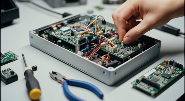
PCB assembly essentials
PCB assembly is about adding electronic parts to the board. This step turns the plain board into a working device. Two main methods are used: surface mount technology (SMT) and through-hole technology (THT). SMT places parts on the board’s surface, making small and modern designs. THT pushes part leads through holes, creating strong connections for tough uses.
Soldering is a key part of assembly. It attaches parts to the board and ensures good electrical links. Advanced soldering methods, like reflow and wave soldering, help make sure everything is done right. Quality checks, like automated optical inspection (AOI) and X-ray inspection, confirm the assembly is correct.
Importance in modern electronics
PCBs are essential for today’s electronics. They allow devices like phones, smartwatches, and car systems to be small and efficient. The need for PCB prototypes has grown because electronics are advancing so quickly. For example, electric and self-driving cars need very reliable PCBs. Also, 5G and IoT technologies require new PCB designs to handle fast data.
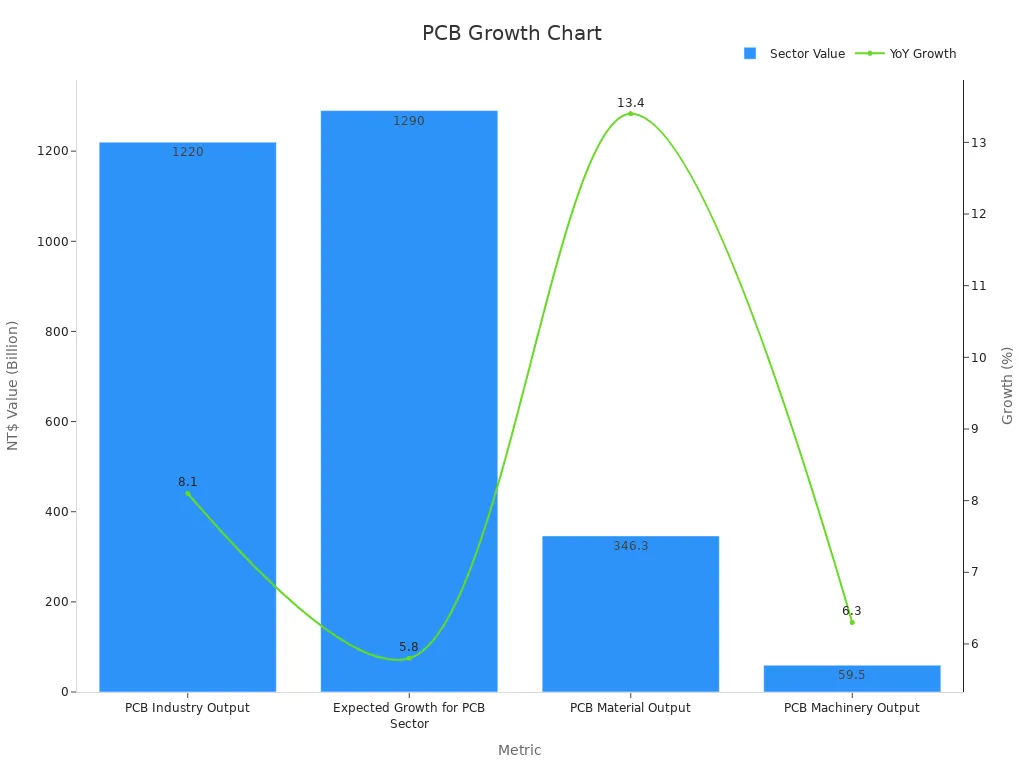
The PCB industry has grown a lot recently. Reports show it reached 1.22 trillion NT$, growing 8.1% in one year. This growth shows how important PCBs are for new technology and meeting the needs of the electronics world.
Key Steps in PCB Manufacturing
Design and layout creation
Making a PCB starts with designing its layout. Special software helps create a plan showing where parts go. It also maps how electrical connections will work. This step ensures the PCB works properly and meets its goals.
Here are some tips to improve your PCB design:
- Use smart layer setups to save money without losing quality.
- Control signals for fast digital and analog designs to avoid issues.
- Test designs early to catch problems and save money later.
- Keep wires short and pair them for better signal flow.
- Balance costs by choosing the right number of layers and materials.
Following these tips helps you make a design that works well and stays within budget.
Material selection and preparation
Picking the right materials is very important for a good PCB. Materials must match the design’s needs, like layers, wire spacing, and special features. Some boards need extra details like flexible parts or dense connections.
Here’s what to think about when choosing materials:
| Factor | What It Means |
|---|---|
| Complexity | Handles layers, wire spacing, special holes, or flexible designs. |
| Materials | Includes things like laminates and copper thickness. |
| Finishes | Surface options like HASL, ENIG, or OSP for different uses. |
| Quality Control | Certifications like ISO 9001 and tools like AOI or X-ray for checking. |
After picking materials, clean them to remove dirt. Make sure the copper is ready for shaping. Clean materials help avoid mistakes and make production smoother.
Etching and patterning
Etching shapes the PCB by removing extra copper. A mask protects the parts that stay, while the rest gets etched away. This step creates the circuits needed for the board to work.
Accuracy is very important here. Mistakes can ruin the PCB’s performance. New methods, like laser etching, make designs more precise. These techniques help create tiny, detailed circuits perfectly.
By mastering these steps, you can make high-quality PCBs. Whether it’s for testing or mass production, following these steps ensures great results.
Drilling and via creation
Drilling is a key part of making a pcb. It makes holes that connect layers for electricity to flow. These holes, called vias, let signals move through the board. Precision is very important because small mistakes can ruin the pcb.
Modern drills use advanced CNC machines. These machines use fast drills or lasers to make accurate holes. Laser drilling is great for tiny vias in dense pcb designs. It makes clean cuts for strong connections.
There are three main types of vias:
- Through-hole vias: Go through the whole board and link all layers.
- Blind vias: Link an outer layer to inner layers but don’t go through the board.
- Buried vias: Stay inside the board and can’t be seen from outside.
Plan via placement carefully during design. This helps signals flow better and avoids problems.
Tip: Use automated tools to check the drilling process. This ensures the vias are correct and prevents costly mistakes.
Plating and finishing
Plating and finishing make the pcb stronger and work better. After drilling, vias and copper parts get a coating. This helps electricity flow and stops rust.
Electroplating is the most common method. It adds a thin metal layer, like copper or gold, to the board. This makes vias stronger and connections reliable. For special uses, finishes like ENIG or HASL are good choices.
Here’s a quick look at popular finishes:
| Finish Type | Key Features | Best For |
|---|---|---|
| ENIG | Stops rust, smooth surface | High-quality uses |
| HASL | Cheap, long-lasting | Everyday pcbs |
| OSP | Eco-friendly, simple to use | Short-term projects |
Finishing also includes adding a solder mask. This layer stops short circuits and makes the board look nice. Green is the most common color, but others are available.
Note: Pick a finish based on your pcb’s purpose. Think about cost, strength, and the environment when deciding.
Electrical testing and quality assurance
Testing ensures the pcb works as planned. It checks all connections and confirms the design is correct. Skipping this step can cause big problems later.
Two common tests are:
- Flying probe testing: Probes check each connection point. It’s good for small batches or prototypes.
- Bed-of-nails testing: Pins test all points at once. It’s faster for large batches.
Quality checks also find physical problems. Tools like AOI and X-ray inspection spot issues like misplaced parts or bad soldering.
Pro Tip: Combine electrical and visual tests for the best results. This ensures your pcb works well and looks good.
By following these steps, you can make great pcbs. Whether it’s a small test or a big project, paying attention to details is key.
Key Steps in PCB Assembly
Component sourcing and preparation
The first step is getting and preparing parts for the pcb. All parts must match the design and meet quality rules. This is important because the pcb‘s performance depends on good parts.
When choosing parts, think about cost, availability, and if they fit the design. Working with a trusted supplier or manufacturer can help you get reliable parts. Many manufacturers now offer services that include finding parts, saving you time.
After getting the parts, preparation starts. Check each part for problems, clean them, and organize them for use. This helps avoid mistakes during assembly and keeps things running smoothly.
Tip: Keep a list of all parts. This helps track them and prevents delays if something runs out.
Surface mount technology (SMT)
SMT is a popular way to assemble pcbs. It places parts directly on the board’s surface. This method makes small, lightweight designs, perfect for gadgets like phones and watches.
First, solder paste is added to the board using a stencil. The stencil ensures the paste goes only where needed. Then, a machine places parts on the board quickly and accurately. These machines can handle many parts in a short time.
Next, the board goes into a reflow oven. The heat melts the solder paste, connecting the parts to the board. Advanced SMT machines also check for mistakes during this process.
Note: SMT works best for making many pcbs or small, modern designs.
Through-hole technology (THT)
THT is another way to assemble pcbs. Unlike SMT, THT puts part leads through holes in the board. This method makes strong connections, great for tough uses like cars or factory machines.
The process starts by placing parts into the holes, either by hand or machine. Then, the leads are soldered to the board. Wave soldering is often used for this. The board passes over melted solder, which bonds the leads to it.
THT takes more time than SMT but is better for big parts or when testing and replacing parts is needed.
Pro Tip: Use both SMT and THT in your design. This combines their strengths and works well for complex pcbs.
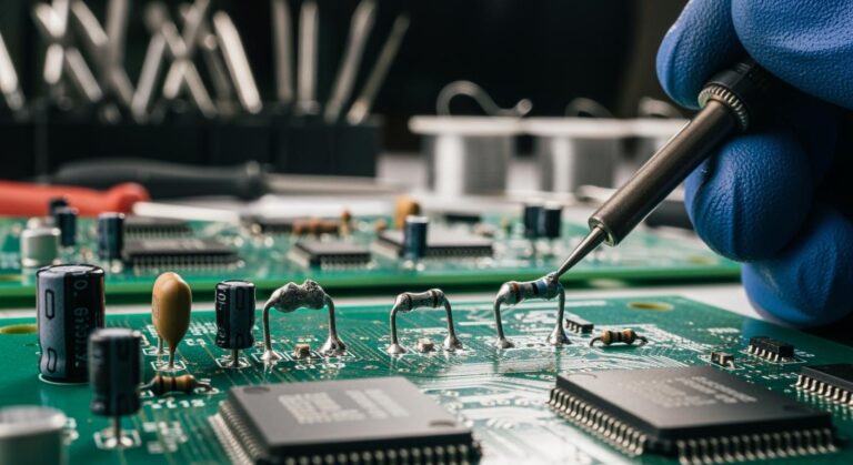
Soldering techniques
Soldering connects parts to the pcb for reliable performance. Different soldering methods are used based on the pcb‘s design and purpose. Each method works best for specific needs.
Reflow Soldering
Reflow soldering is common for SMT designs. First, solder paste is added to the pcb. Then, parts are placed, and the board is heated in a reflow oven. The heat melts the paste, bonding parts to the pcb. This method is great for making many small, modern pcbs.
Wave Soldering
Wave soldering is used for THT designs. The pcb moves over melted solder, which attaches part leads to the board. This method is fast and works well for strong, heavy-duty connections in large batches.
Selective Soldering
Selective soldering targets specific areas of the pcb. A nozzle applies solder only where needed. This method is perfect for complex pcbs with both SMT and THT parts.
Hand Soldering
Hand soldering is done by skilled workers using a soldering iron. It’s slower but useful for fixing problems or making custom pcbs. This method is often used for small projects or repairs.
Tip: Pick the right soldering method for your pcb. Good soldering ensures the pcb works well and lasts long.
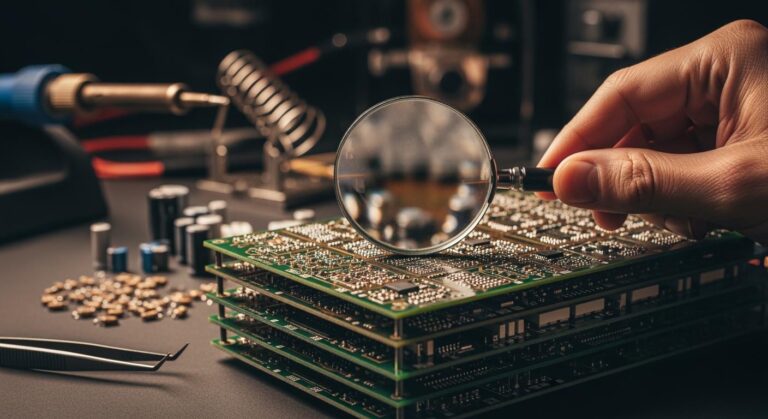
Inspection and testing
Inspection and testing check if the pcb is made correctly. These steps find problems early, ensuring the pcb works as planned. New tools in 2025 make these checks faster and more accurate.
Solder Paste Inspection (SPI)
SPI uses 3D tools to check solder paste. It ensures the paste is applied evenly. This prevents problems like too much or too little solder, which can cause issues.
Automated Optical Inspection (AOI)
AOI uses cameras to find problems like misplaced parts or bad solder joints. It also tracks patterns to fix issues quickly. AOI is great for checking many pcbs at once.
Flying Probe Testing
Flying probe testing is good for small batches or prototypes. Probes test points on the pcb to check connections and parts. Reports show any problems so they can be fixed fast.
In-Circuit Testing (ICT)
ICT checks if the pcb works as it should. It tests each part and connection. This method is fast and works well for making many pcbs.
| Inspection Method | Key Features | Benefits for Quality Assurance |
|---|---|---|
| Solder Paste Inspection (SPI) | 3D Tools, Real-Time Feedback, Even Solder Check | Ensures solder is applied correctly |
| Automated Optical Inspection (AOI) | Cameras, Finds Defects, Tracks Patterns | Fixes problems early for better results |
| Flying Probe Testing | Probes Test Points, Detailed Reports | Checks small batches or prototypes quickly |
| In-Circuit Testing (ICT) | Tests Each Part, Fast for Large Batches | Makes sure the pcb works perfectly |
Pro Tip: Use more than one inspection method. This helps catch all problems and ensures the pcb meets high standards.
Innovations in PCB Manufacturing Assembly in 2025
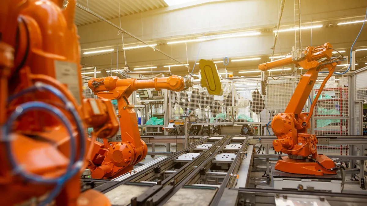
Automation and robotics
Automation and robotics have changed how PCB assembly works in 2025. Robots now do jobs like soldering, drilling, and placing parts. They work faster and make fewer mistakes than humans. Special robots called “cobots” team up with people. Cobots make the process safer and help with tricky tasks.
Robotic arms use sensors to keep quality high. They fix problems like misaligned parts right away. This accuracy is crucial for modern devices, where small mistakes can cause big issues. Automation also lets factories run all day and night. This helps meet deadlines without lowering quality.
AI-driven design and quality control
AI has made designing and checking PCBs much better. It speeds up design and makes it more accurate. For example:
- Designs are finished 42% faster.
- Accuracy has improved by 81%.
- Quality has reached an impressive 95%.
AI tools also improve quality checks. They find problems in real-time and fix them quickly. Predictive tools warn about future issues, reducing downtime. These upgrades save money and make PCB manufacturing more efficient.
Smart factories using AI now set higher standards. They produce more while keeping quality excellent.
Eco-friendly materials
Sustainability is now a must in PCB manufacturing. In 2025, you can use eco-friendly materials that are better for the planet. Examples include biodegradable laminates and lead-free solder. These meet strict rules while still working well.
Recycling is also important. Factories recover metals like copper and gold from old PCBs. This cuts waste and reduces the need for new materials. Using these methods helps the environment and saves money.
Tip: Choose suppliers who focus on sustainability. This supports global goals and boosts your brand’s image.
Advanced inspection technologies
In 2025, inspection tools have greatly improved. They help ensure every PCB meets top standards. These tools find problems faster and more accurately, reducing mistakes and boosting efficiency.
A major improvement is the use of 3D Automated Optical Inspection (AOI). This system checks each layer of the PCB for issues like misplaced parts or bad soldering. Unlike older 2D systems, 3D AOI gives a full view of the board. It catches tiny details that might be missed in dense designs.
Another big change is adding machine learning algorithms to inspections. These smart systems learn from past data to predict future problems. For example, if a certain soldering pattern caused issues before, the system warns you during production. This saves time and cuts down on waste.
Tip: Use both 3D AOI and machine learning together. This combo ensures your PCBs are perfect in looks and function.
Lastly, X-ray inspection systems are now more advanced. They find hidden problems like gaps in solder joints or cracks inside the board. These tools make sure even the most complex PCBs are reliable.
Miniaturization and high-density interconnects
Smaller, stronger devices need tiny PCBs. In 2025, you can make very compact boards without losing performance. High-density interconnects (HDI) are key to this progress.
HDI lets you fit more parts into less space. Features like microvias and stacked vias help route signals in multi-layer boards. This is important for gadgets like phones, wearables, and medical tools where space is tight.
To shrink PCBs, manufacturers use ultra-thin laminates and new materials. These keep the board strong while making it thinner. Laser drilling is now common for making precise microvias, ensuring good connections in tight spaces.
Note: Small PCBs create more heat. Plan for cooling to avoid performance issues.
Miniaturization also changes how PCBs are assembled. Surface mount technology (SMT) now handles tiny parts like 01005 packages. These small pieces need exact placement and soldering, which advanced robots can do well.
By using miniaturization and HDI, you can build modern devices that meet today’s needs.
Challenges and Solutions in PCB Processes
Keeping costs under control
Cutting costs in PCB production needs smart planning. Use materials wisely and improve how things are made. Choose cheaper materials that still work well for your design. This helps lower costs without losing quality. Using machines to automate tasks also saves money by reducing mistakes and labor costs.
Buying parts in bulk is another way to save. Ordering more at once often means getting discounts. Working with trusted suppliers keeps prices steady and avoids sudden cost increases.
Tip: Follow design-for-manufacturing (DFM) rules. This makes production easier and avoids extra costs.
Solving environmental problems
Caring for the environment is now very important in PCB making. Use green materials like lead-free solder and biodegradable laminates. These follow eco-rules and make your process better for the planet.
Recycling is also key. Get metals like copper from old PCBs to cut waste and save money. Use energy-saving machines to lower your impact on the environment and reduce costs.
Note: Work with eco-friendly suppliers. This improves your brand and supports global green goals.
Making complex designs reliable
Complicated PCB designs need to work well every time. Start by making sure the design is strong from the beginning. Use special tools to find problems early and avoid failures later.
Testing is very important for reliability. Use methods like in-circuit testing (ICT) and automated optical inspection (AOI). These tests catch mistakes before the PCB is finished, ensuring high quality.
Pro Tip: Add extra pathways in your design. This keeps the PCB working even if something goes wrong.
Overcoming supply chain disruptions
Problems in the supply chain can delay PCB production and raise costs. In 2025, these issues are harder to handle due to global challenges and rising demand for parts. But, there are ways to reduce risks and keep production smooth.
- Work with many suppliers: Depending on one supplier is risky. Use suppliers from different areas to keep materials coming. This lowers the chance of delays from local problems.
- Use inventory tools: Smart software tracks parts and predicts shortages. It helps you plan ahead and avoid rushing to find parts at the last minute.
- Buy locally when possible: Getting materials nearby cuts shipping time and avoids delays. It also makes the process faster.
- Form strong partnerships: Work closely with suppliers and agree on long-term deals. These deals often give you priority for important parts during shortages.
Tip: Predictive tools can warn you about supply problems early. This helps you prepare before issues grow bigger.
By following these steps, you can protect your PCB production and keep your products reliable.
Adapting to rapid technological changes
Technology in 2025 is changing fast, and staying updated is key. Adapting quickly helps you stay ahead in PCB manufacturing and assembly.
- Keep learning: Train your team on new tools and methods often. This keeps them ready for changes and aware of the latest trends.
- Choose flexible tools: Buy machines and software that can grow with your needs. For example, modular systems let you add features without replacing everything.
- Team up with tech leaders: Work with companies creating new technology. These partnerships give you early access to advanced tools and ideas.
| Strategy | Benefit |
|---|---|
| Keep learning | Keeps your team skilled and updated |
| Flexible tools | Saves money and adjusts to future needs |
| Tech partnerships | Brings new ideas and advanced solutions |
Note: Stay aware of new trends like AI-based PCB design and better inspection tools. This keeps you competitive in a fast-changing market.
By using these ideas, you can improve your PCB production and stay successful as technology grows.
In 2025, making and assembling PCBs is changing electronics. New eco-friendly methods match the need for energy-saving PCBs. These are important for solar and wind power systems. These changes improve how devices work and keep them reliable. Companies like King Field PCB use these ideas to make strong and affordable products. Learning about these updates helps you stay ahead in this fast-changing industry.
FAQ
What is the difference between SMT and THT in PCB assembly?
SMT puts parts on the board’s surface. It’s great for small designs. THT pushes part leads through holes for stronger connections. Use SMT for gadgets like phones. Use THT for tough devices like factory machines.
How does AI improve PCB manufacturing in 2025?
AI makes designing faster and more accurate. It spots problems early and fixes them quickly. AI also improves quality checks, saving time and money. These upgrades make production smoother and cheaper.
Are eco-friendly materials reliable for PCB production?
Yes, green materials like lead-free solder work well. They are strong and meet industry rules. These materials last long and help protect the planet.
What are HDI PCBs, and why are they important?
HDI PCBs fit more parts in less space. They use tiny holes like microvias to connect layers. These boards are perfect for small devices like smartwatches and medical tools.
How can you prevent supply chain disruptions in PCB manufacturing?
Work with many suppliers to avoid delays. Use tools to track parts and predict shortages. Build strong supplier relationships for steady material access during busy times.