What Are HDI PCBs and Their Key Applications
High-Density Interconnect (HDI) PCBs are changing modern electronics. They help make small, powerful designs work well. Unlike regular PCBs, HDI PCBs use special methods like laser-drilled tiny holes and thin lines. This makes them very reliable and able to fit more circuits. These features let makers build smaller, lighter gadgets without losing performance.
The importance of HDI technology is clear from its rising demand.
- The HDI PCB market is expected to grow from USD 16.11 Billion in 2024 to almost USD 39.91 Billion by 2032, with a yearly growth rate of 12%.
- Smaller sizes, better efficiency, and more use in cars are key reasons for this growth.
These improvements make HDI PCBs very important for the future of electronics. They help create devices that are small and very dependable.
Key Takeaways
- HDI PCBs help make smaller and stronger gadgets using special methods like tiny holes and thin wires.
- The HDI PCB market is growing fast and may reach about USD 39.91 billion by 2032 because people want smaller and better technology.
- These boards work better, send signals faster, and fit more circuits, which is why they are great for things like smartphones and medical tools.
- HDI PCBs are built to handle tough conditions, making them reliable for important fields like cars, planes, and healthcare.
- Even though HDI PCBs cost more to make because they are complex, their small size and great performance make them important for modern technology.
Understanding HDI PCBs
What is an HDI PCB?
An HDI PCB is a special type of circuit board. It is made to handle more wiring and complex circuits in less space. Unlike regular PCBs, HDI PCBs use advanced methods like microvias, blind vias, and buried vias. These help connect layers and save space. They have thin lines, slim materials, and many layers. This makes them perfect for small, high-performance devices.
With HDI technology, more parts can fit into smaller spaces. This is why it’s used in gadgets like smartphones, wearables, and medical tools. For example, microvias are tiny holes, less than 0.008 inches wide. They link layers of the board while keeping it compact. This has changed how high-density PCBs are made, helping meet the need for smaller, better devices.
Key Elements of HDI PCB Design
HDI PCB design has unique features that set it apart. These include:
- Microvias: Tiny holes that connect layers and improve signals.
- Blind and Buried Vias: These connect layers without going through the whole board.
- Sequential Lamination: Layers are built one at a time for complex designs.
- Fine Line Traces: Very thin lines, as small as 0.005 inches, increase circuit density.
Rules like IPC-2315 and IPC-2226 guide HDI PCB designs. IPC-2315 explains microvia structures, while IPC-2226 gives rules for materials and line sizes.
Why HDI Matters in Modern Electronics
HDI technology is vital for today’s electronics. It solves problems like making devices smaller, faster, and more reliable. Here’s why it’s important:
- Better Electrical Performance: Signals move faster and work more reliably.
- Higher Circuit Density: Microvias and thin lines allow more features in less space.
- Strong and Reliable: These boards last long, even in tough conditions like cars or planes.
For example, HDI PCBs are key in 5G networks, where fast data and low delays are needed. They also help make IoT devices, which need small, powerful designs.
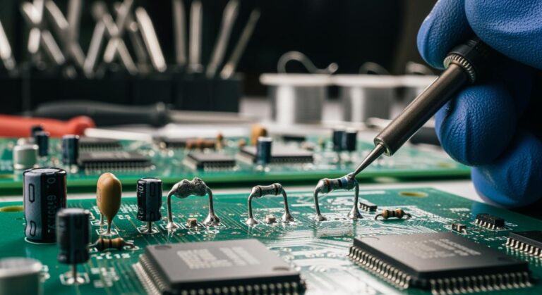
Making HDI PCBs is a detailed process. It uses laser drilling, plating, and layering steps. These ensure the boards meet the needs of modern tech, from gadgets to space tools.
Features and Advantages of HDI PCBs

High Wiring Density and Microvias
HDI technology helps fit more wiring into small spaces. Microvias, tiny holes connecting board layers, save space. These are smaller than regular vias, allowing more parts to fit. This is useful for gadgets like smartphones and wearables with limited room.
HDI PCBs improve signal quality with shorter paths and less noise. This makes devices work faster and more reliably. They are great for high-speed data and dependable performance needs.
Better Performance and Signal Quality
HDI PCBs improve how signals move through the board. Their design keeps signals clear and reduces loss or distortion. This is important for things like 5G networks needing fast, steady communication.
Good signal quality lowers errors in sending data. Blind and buried vias help arrange the board better, boosting its performance. This makes HDI PCBs ideal for precise industries like aerospace and healthcare.
Small and Lightweight Design
HDI lets you make small, light boards that still work well. By adding layers and thin lines, more features fit in less space. This is helpful for portable gadgets where size and weight matter.
Small HDI PCBs are also strong and last longer. With better layouts and fewer stresses, they handle tough conditions. Whether for home gadgets or industrial tools, their lightness is a big advantage.
Strength and Dependability in Tough Conditions
HDI PCBs work well in harsh environments. They are built to handle heat, stress, and moisture. These boards keep working even in the toughest situations.
Manufacturers test HDI PCBs to ensure they are reliable. Tests mimic real-world conditions to check strength and performance. Below is a table showing key tests and their results:
| Test Type | Purpose | How It’s Done | What It Shows |
|---|---|---|---|
| Environmental Stress | Tests how PCBs handle temperature changes | Exposed to temperatures from -40°C to +85°C | Checks solder joints, component strength, and durability |
| Humidity Testing | Measures resistance to water and corrosion | Placed in humid and warm conditions | Finds risks of corrosion, delamination, or water damage |
| Vibration Testing | Checks strength against shaking or movement | Vibrated at different speeds and intensities | Tests solder joints, component attachment, and structure |
| Shock Testing | Tests resistance to sudden impacts | Dropped or hit with strong force | Shows strength of components and ability to handle stress |
These tests prove HDI PCBs can handle heat, shaking, and water damage. For example, temperature tests ensure solder joints stay strong despite heat changes. Vibration and shock tests show the board can survive bumps during use or transport.
HDI PCBs are great for tough jobs. They work well in cars, planes, and factories. These boards make sure devices run smoothly without breaking down.
HDI PCBs vs Standard PCBs
Design and Manufacturing Differences
HDI PCBs and standard PCBs are made differently. HDI PCBs use advanced methods like microvias, blind vias, and buried vias. These allow more parts to fit in smaller spaces. Standard PCBs use through-hole vias, which take up more room. HDI PCBs also use sequential lamination to build many layers. Standard PCBs usually have fewer and simpler layers.
Here’s a table showing the main differences:
| Feature | Standard PCB | HDI PCB |
|---|---|---|
| Cost | Cheaper | More expensive |
| Layer Count | 1-16 layers | Often more than 8 layers, built step-by-step |
| Feature Size | Bigger lines and spaces | Smaller lines, spaces, and microvias |
| Via Technology | Through-hole vias | Microvias, blind vias, buried vias |
| Density | Fewer parts in a given space | Fits more parts in less space |
| Performance | Good for simple uses | Great for fast and complex devices |
| Application | Basic gadgets, low-speed devices | Phones, wearables, medical tools, fast networks |
| Manufacturing Complexity | Easier to make | Harder to make, needs advanced steps |
| Turnaround Time | Faster to produce | Slower to produce |
These differences explain why HDI PCBs are chosen for advanced devices. They cost more but work better for high-tech needs.
Performance and Cost Comparisons
HDI PCBs perform better than standard PCBs. They are great for fast devices like 5G phones and IoT gadgets. Their design keeps signals clear and reduces errors. Tests like thermal cycling and bending checks prove they are strong. Special tests also show they handle high-speed signals well.
But HDI PCBs are pricier to make. They need special materials and skilled workers. The process takes longer and costs more. Even so, their small size and great performance make them worth it for important devices.
Applications of HDI Technology vs Standard PCBs
HDI PCBs are used in more advanced ways than standard PCBs. Standard PCBs are fine for simple gadgets and low-speed devices. HDI PCBs are found in phones, wearables, and medical tools. They are also used in planes and cars, where reliability is key.
HDI PCBs make smaller, lighter boards with more parts. This is essential for modern technology. Standard PCBs are cheaper and good for basic designs. But they can’t match HDI PCBs for speed or size.
Types of HDI PCBs
1-N-1 HDI PCBs
1-N-1 HDI PCBs are simple high-density designs. They have one layer of microvias on each side of the core. This helps with neat layouts and better routing. These PCBs are great for medium-complexity tasks needing good performance.
They allow more parts to fit, making devices work better. Shorter signal paths improve how signals travel, reducing errors. This makes them perfect for fast digital and RF uses. Fewer connections mean fewer problems and better heat control. But, making them needs careful planning and advanced tools like laser drills.
| Feature | Description |
|---|---|
| Increased functionality | Handles complex designs with more parts. |
| Improved signal integrity | Shorter paths mean fewer losses and less noise. |
| Enhanced reliability | Fewer connections make them stronger and manage heat better. |
| Cost optimisation | Smaller size saves material and shipping costs. |
2-N-2 HDI PCBs
2-N-2 HDI PCBs are more advanced. They have two layers of microvias on each side of the core. This allows even more parts and better signal paths. These PCBs are ideal for small, fast devices.
Compared to regular PCBs, they fit more parts in less space. Microvias, blind vias, and buried vias help save room. But making them is harder and costs more. It needs steps like laser drilling and layering.
| Feature | HDI PCBs | Traditional PCBs |
|---|---|---|
| Layer Stack-Up | Complex, with many layers. | Simple, with fewer layers. |
| Signal Routing Density | High, with efficient paths. | Low, with fewer paths. |
| Miniaturisation | Small, with more parts. | Bigger, with fewer parts. |
Any-Layer HDI PCBs
Any-layer HDI PCBs are the most advanced type. They let any two layers connect directly. This removes the need for fixed via paths. These PCBs are great for modern gadgets like phones and medical tools.
Thinner materials and narrow lines improve performance. They help control signals and reduce issues with vias. But, fitting so many parts makes power and heat harder to manage. Good power design is key to keeping these PCBs reliable.
Applications of HDI PCBs
Consumer Electronics and Wearables
HDI PCBs are crucial for modern gadgets and wearables. They help make small, powerful devices like phones, tablets, and smartwatches. These gadgets need tiny, light boards to support fast processors, better connections, and longer battery life.
For example, fitness trackers like Fitbit Flex use thin, bendable PCBs. This makes them comfy to wear and saves battery power. Similarly, smart clothes like Levi’s Commuter x Jacquard jacket have washable PCBs. These allow touch controls while staying flexible. These examples show how HDI PCBs combine technology with everyday items.
| Application Type | Case Study Description |
|---|---|
| Fitness Tracking Devices | Fitbit Flex uses a thin, flexible PCB for comfort, long battery life, and Bluetooth syncing. |
| Smart Clothing | Levi’s Commuter x Jacquard jacket has a washable PCB for touch controls, blending fashion and tech. |
| Advanced Prosthetics | Ottobock’s bionic limbs use small PCBs for smooth movement and easy control, helping people with disabilities. |
As people want smaller, smarter gadgets, HDI PCBs are in higher demand. This shows how important they are for the future of wearables and portable devices.
Automotive and Electric Vehicles
Cars and electric vehicles (EVs) use HDI PCBs for advanced systems. These include self-driving features, driver-assistance tools, and EV battery controls. Their small size and strong performance make them perfect for tight spaces in vehicles.
For instance, Tamura Corporation makes special inks for precise ADAS modules. Fujifilm creates inks that shrink battery PCBs while keeping them efficient. These examples show how HDI PCBs help make safer and smarter cars.
| Company | Advantage Description |
|---|---|
| Tamura Corporation | Makes conductive ink for 25μm line spacing in ADAS modules. |
| Fujifilm | Produces inks that cut battery PCB size by 40% while boosting performance. |
HDI PCBs are also used in car entertainment systems, GPS units, and V2X communication. These uses highlight how HDI technology drives progress in the car industry.
Healthcare and Medical Devices
HDI PCBs are vital for small, reliable medical devices. These devices need accurate signals and low power use, making HDI technology essential. They are found in health monitors, diagnostic tools, and advanced prosthetics.
For example, the Zio Patch uses skin-friendly PCBs to track heart activity. These PCBs are made for comfort and low power use. Advanced prosthetics, like Ottobock’s, rely on compact PCBs for smooth movement and control.
| Application Type | Case Study Description |
|---|---|
| Medical Monitoring Devices | Zio Patch uses a biocompatible PCB for heart monitoring, designed for comfort and low power use. |
| Advanced Prosthetics | Ottobock’s bionic limbs use small PCBs for natural movement and easy control, improving life for users. |
| Child and Elderly Care Monitoring | AngelSense GPS Tracker has a strong PCB with GPS and voice features, ensuring safety and communication for vulnerable groups. |
As the need for portable medical devices grows, HDI PCBs enable new solutions. They help improve healthcare and make life better for patients.
Aerospace and Defence Systems
HDI PCBs are crucial for aerospace and defence systems. These industries need parts that are precise, reliable, and compact. They must also handle tough conditions like heat, shaking, and radiation. HDI technology helps make strong circuit boards that meet these needs.
In aerospace, HDI PCBs are used in planes and satellites. They are found in systems like avionics, satellite communication, and navigation tools. Their small size lets engineers add advanced features in tight spaces. For example, microvias and blind vias improve signals, ensuring smooth communication during important tasks.
Defence systems also use HDI PCBs for modern equipment. Radar systems, missile controls, and secure communication devices depend on these boards. HDI PCBs are tough and work well in harsh places like battlefields or high altitudes. Their lightweight design also helps military vehicles and drones perform better.
HDI PCBs are key to innovation in aerospace and defence. They help make smaller, smarter devices that improve safety and performance in these fields.
Industrial IoT and Smart Devices
Industrial IoT and smart devices are changing factories, transport, and homes. HDI PCBs are vital for these changes. They provide small, powerful electronics for connected systems.
In industrial IoT, HDI PCBs allow sensors and communication tools to fit into small devices. This helps factories monitor and control processes in real time. Flexible circuit boards make it easier to use IoT devices in different places. They also ensure smooth data sharing across networks.
Smart devices like home systems and wearables also use HDI PCBs. Their small size lets engineers add features like wireless connections and AI. Microvias and multi-layer designs improve functions while keeping devices light and portable.
The demand for HDI PCBs in IoT and smart devices is growing. Companies use this technology to add more features in smaller spaces. Research shows plastic circuits for IoT devices will grow, showing HDI’s importance in modern electronics.
HDI PCBs help create small, high-performing devices for IoT and smart tech. Their flexibility and strength make them essential for connected systems that improve work and life.
Challenges and Limitations of HDI PCBs
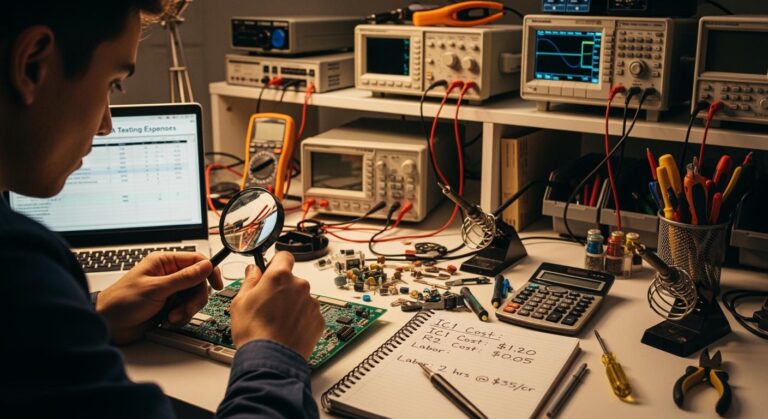
Complexity in Manufacturing
Making HDI PCBs is tricky and needs advanced tools and skilled workers. Steps like laser drilling and layering must be precise, or mistakes can happen. Designers and engineers must work together to reduce errors and make production smoother.
- Higher Manufacturing Costs: Special machines like laser imaging make production expensive.
- Design for Manufacturability (DFM): Engineers create test setups to fix assembly problems.
- Prototyping Importance: Testing early helps find mistakes, saving time and money.
Chrys Shea, an expert, says testing and design improvements are key. These steps ensure HDI PCBs work well and stay reliable for modern devices.
Higher Costs and Resource Requirements
Making HDI PCBs costs more because of advanced tools and materials. Steps like drilling and layering are complex, and copper prices can change, affecting costs. Rules about the environment also add to expenses.
| Cost Factor | Description |
|---|---|
| Processing Complexity | Laser drilling and other steps make production harder and pricier. |
| Material Price Fluctuation | Copper prices can go up and down, changing overall costs. |
| Transportation Strategies | Good shipping plans can lower costs for big orders. |
| Market Dynamics | Supply and demand affect prices and availability. |
| Regulatory Compliance | Following environmental rules can raise costs and limit materials. |
Manufacturers must balance cost and quality. Though HDI PCBs perform better, making them needs big investments in tools and skilled workers.
Design and Testing Challenges
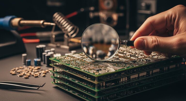
Designing HDI PCBs is hard and needs careful planning. Engineers must solve problems like tiny holes, layered designs, and heat control. Testing methods like optical checks and X-rays are important for quality.
- Microvia Formation: Plasma tools help make tiny holes stick better and avoid damage.
- Sequential Lamination: Adding layers one by one can cause changes in performance.
- Thermal Management: Special ways are needed to handle heat from packed circuits.
- Quality Assurance Testing: Tests like flying probes and environmental checks ensure reliability.
Prototyping is crucial to spot design issues early. Engineers test how the board works and check if it lasts in tough conditions. These steps help make sure HDI PCBs meet high standards and work well.
HDI PCBs have changed electronics by making smaller, better devices. They help create compact gadgets without losing any features. Better signal quality means faster and more reliable communication. This makes them essential for things like smartphones. HDI PCBs are used in many areas, from medical tools like pacemakers to cars like Tesla. They also work well in tough conditions, proving useful in military and space systems. Plus, their smart design cuts down layers but keeps quality high, making them a good choice for advanced uses.
| Key Features | Benefits | Uses |
|---|---|---|
| Miniaturisation | Helps make small, powerful devices | Medical tools (e.g., pacemakers) |
| Better signal quality | Shorter paths improve speed and reliability | Consumer gadgets (e.g., smartphones) |
| Versatility | Works in many industries | Cars (e.g., Tesla vehicles) |
| High durability | Handles tough environments | Military gear (e.g., defence tools) |
| Cost-efficient | Fewer layers but same quality | Space systems |
Using HDI PCBs helps create smarter, faster technology for many industries.
FAQ
What does HDI mean in HDI PCBs?
HDI means High-Density Interconnect. It describes circuit boards with special features like tiny holes and thin lines. These features allow smaller designs and better performance for modern gadgets.
How are HDI PCBs different from regular PCBs?
HDI PCBs use tiny holes and hidden connections to save space. Regular PCBs use bigger holes that take up more room. HDI boards also have thinner lines and more layers for advanced uses.
Can HDI PCBs handle tough conditions?
Yes, HDI PCBs are made to survive extreme situations. They are tested for heat, moisture, shaking, and sudden impacts. This makes them perfect for planes, cars, and military equipment.
Why do HDI PCBs cost more to make?
HDI PCBs need special tools like laser drills and skilled workers. The process includes tricky steps like adding layers and making tiny holes. These make them more expensive than regular PCBs.
Do HDI PCBs improve signal quality?
Yes, HDI PCBs have shorter paths for signals to travel. This reduces noise and keeps signals clear. They are great for fast devices like 5G phones and smart gadgets.