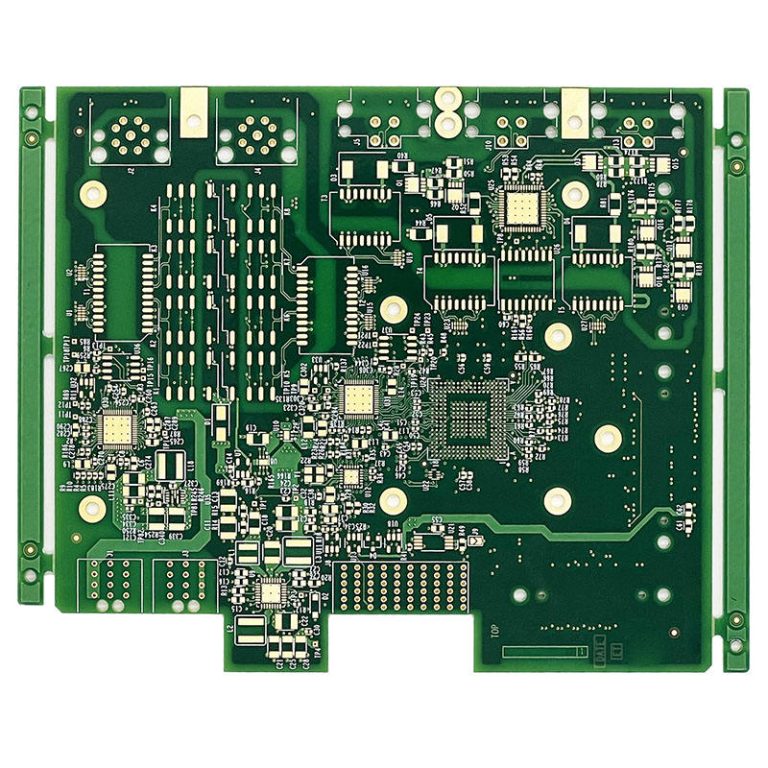
You see multilayer PCBs in almost every modern device now. These circuit boards have layers stacked together. They use copper and insulation in turns to make tricky paths. Multilayer printed circuit boards let more wires fit in small spaces. They help signals stay strong and clear. This lets phones and medical tools work faster.
- The multilayer PCB market is growing in North America. New technology and more need from phone and car companies help this growth.
- Multilayer and high-density interconnection PCBs give more choices and fit more circuits. These things are important for small electronics.
Key Takeaways
- Multilayer PCBs fit more circuits into a small space. This makes them great for things like smartphones and tablets. These boards have many copper layers. The layers help signals stay strong and clear. They also cut down on interference. This means the boards work better. Multilayer PCBs are harder and cost more to make. But they are stronger and work better. Smart ways to guide signals, like ground planes, keep signals safe. They also lower noise in multilayer PCBs. Many industries use these boards. Telecommunications, cars, and medical devices need them. They help new technology fit in small spaces.
PCB Types Compared
Single-Layer PCB
Single-layer PCBs are used in simple electronics. These boards have one copper layer on one side. People use them for things like calculators and LED lights. They are cheap to make and good for easy circuits.
| Type of PCB | Structure Description | Key Features |
|---|---|---|
| Single-Sided | Has one copper layer on one side of the board. | Easy and cheap to make; works for simple uses. |
Double-Sided PCB
Double-sided PCBs give you more ways to connect parts. They have copper on both sides of the board. Small holes called vias link the two sides. This helps fit more parts and wires in less space. You see these boards in power supplies, control panels, and some audio gear.
| Type of PCB | Structure Description | Key Features |
|---|---|---|
| Double-Sided | Has copper on both sides, with vias to connect them. | Lets you add more parts; harder to make than single-sided; costs more. |
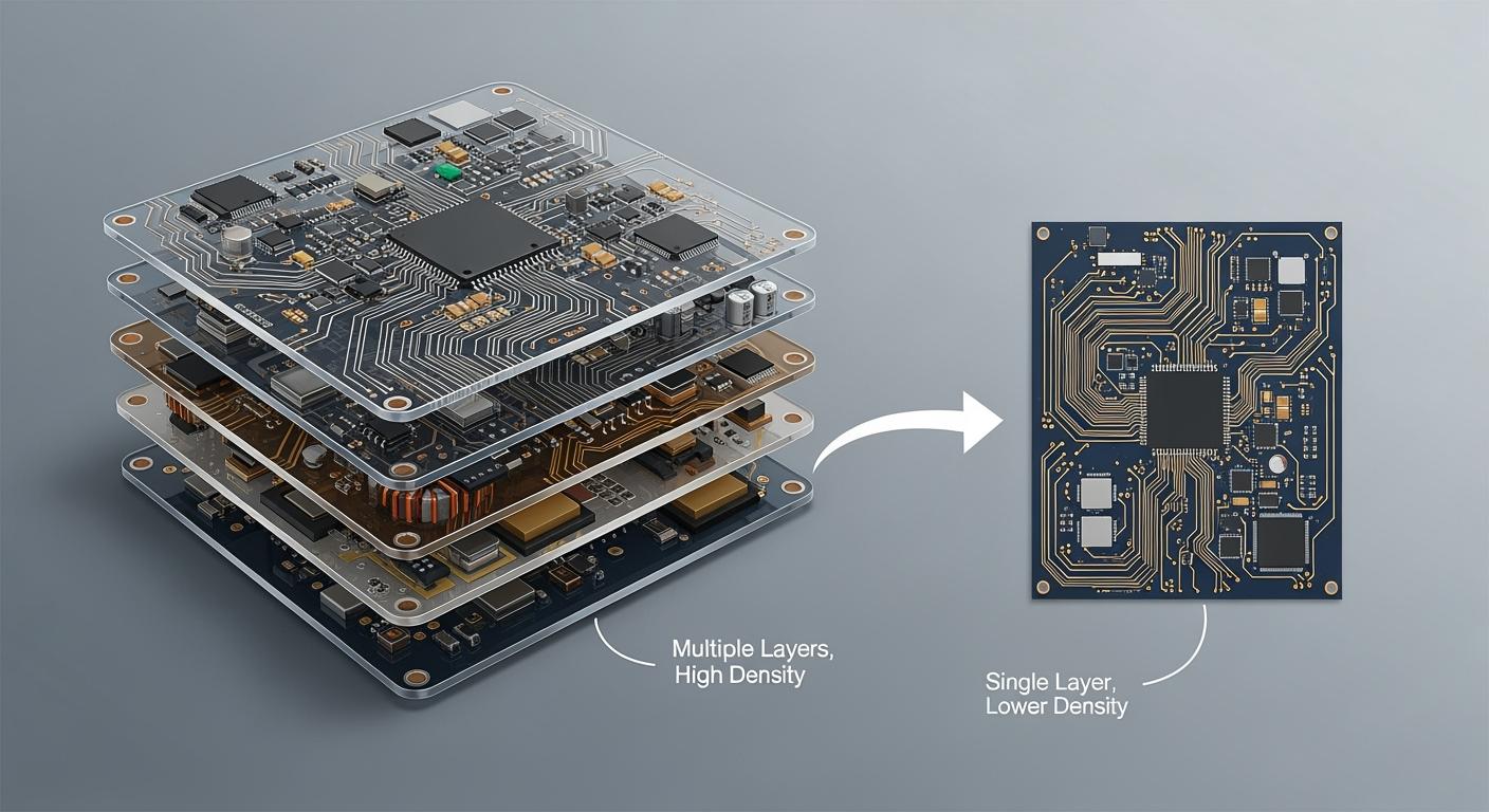
Multilayer PCB Structure
Multilayer PCBs are special because they stack three or more copper layers. There is insulation between each layer. These boards are in advanced things like smartphones and computers. The extra layers let you run many wires without making the board bigger. This means you can build hard circuits that stay small and light.
| Type of PCB | Structure Description | Key Features |
|---|---|---|
| Multilayer | Has three or more copper layers pressed together with prepreg. | Handles tough circuits; strong and long-lasting because of how it is made. |
Note: Most multilayer PCBs for business have 4 to 16 layers. Some special boards have 30, 50, or even over 100 layers. More layers make the board harder and more expensive to build.
| Feature | Single-Sided PCB | Double-Sided PCB | Multi-Layer PCB (4-Layer Example) |
|---|---|---|---|
| Circuit Density | Low | Medium | High |
| Design Complexity | Very Low | Medium | MediumHigh to Very High |
| Size & Weight | Larger, heavier | Smaller than single-layer | Smallest and lightest |
You should know that more layers in a multilayer PCB cost more money. Each layer needs extra materials and careful work to line up. Hard printed circuit board designs, like high-density interconnects, are more expensive to make.
- Multilayer PCBs can have up to 100 layers for special uses.
- Most products use 4, 6, or 8 layers to balance cost and performance.
- More layers make building the board harder and pricier.
When you look at all types, multilayer PCBs fit the most wires and are the smallest. You get more ways to design, but you also pay more and need harder steps to make them.
How Multilayer PCBs Work
Layer Construction
Multilayer PCBs are made by stacking thin layers. Each layer does something important. Makers use copper sheets and special prepregs and cores. They put these materials in a sandwich-like stack. Copper layers move signals and power. Insulation keeps layers apart and safe from problems.
Making multilayer PCBs takes careful steps. First, workers put the circuit design on each copper layer. They clean and coat the core, then add the pattern. Next, they stack layers with prepreg between them. Heat and pressure stick everything together. This step makes the board strong and holds layers tight. After that, tiny holes called vias are drilled. These holes link layers so signals can move up and down. Workers cover the holes with copper to make sure signals travel well. A solder mask and printed labels are added for safety and easy reading.
Tip: Putting power and ground layers close to signal layers helps keep signals steady and stops interference. Makers control layer spacing to balance how well the board works and how easy it is to build.
Multilayer PCBs use copper for circuits, prepreg for sticking, and cores for strength. The heat and pressure make a solid, layered PCB. You get a board that can handle hard designs and fast speeds.
Signal Routing in Multilayer PCB
Smart signal routing helps multilayer PCBs work well. Signals move through lines on each layer. Vias let signals jump between layers. Vias are tiny tunnels that connect layers, making paths short and saving space.
When routing signals, you want to stop interference and crosstalk. You can space lines apart to keep signals clean. Ground planes give signals a safe way back, lowering noise. Differential pairs help fast signals by blocking common noise. Keep lines straight and avoid sharp turns to stop signal trouble.
Here are some ways to route signals in a multilayer PCB:
- Use ground planes for less noise and better signals.
- Space lines apart to lower crosstalk.
- Put fast signals between electrode layers for shielding.
- Place decoupling capacitors near power pins to block noise.
- Use microvias in tight designs for short, direct paths.
| Routing Technique | Benefit |
|---|---|
| Ground planes | Lower noise, better signal quality |
| Trace spacing | Less crosstalk, cleaner signals |
| Differential pairs | Blocks common noise |
| Controlled impedance | Stops reflections, keeps signals sharp |
| Microvias | Shorter paths, better for fast signals |
Designing vias for fast boards means using small vias and microvias. These choices keep signals strong and cut down bad effects. You split fast and slow signals to avoid noise. Shielding and smart layer order protect signals.
Note: Makers use insulation layers with set thickness and smart stacking to keep signals apart and strong. They do not put signal layers next to each other, using planes between to stop interference.
You get a multilayer PCB that moves signals well, keeps interference low, and supports hard circuits. The layers, vias, and routing tricks all help modern electronics work.
Multilayer PCB Advantages & Drawbacks
Benefits of Multilayer PCB
You get many good things from multilayer PCBs. These boards let you put more circuits in a small space. That is why tablets and smartwatches use them. The layers help make strong and fast circuit layouts. You can send signals well and keep them clear.
Multilayer PCBs have special power and ground planes. These layers give power smoothly and stop voltage drops. Shielded signal layers block interference. This helps your device work better at high speeds and in noisy places.
Here is a table that shows how multilayer PCBs and single-layer boards are different:
| Issue | Single-Layer PCBs | Multilayer PCBs |
|---|---|---|
| Signal Integrity | Faces limitations in high-frequency apps. | Controlled impedance routing improves integrity. |
You also get better heat control. Inside copper layers spread heat out. Thermal vias and hidden copper move heat away from hot spots. This keeps your PCB safe and working well.
Some main advantages of multilayer PCBs are:
- Power is cleaner with special planes
- Shielded signal layers stop interference
- High-density interconnects fit hard circuits
- Internal copper layers help heat move away
Tip: Multilayer PCBs let you make smaller, lighter, and stronger devices.
Limitations and Challenges
There are some problems with multilayer PCBs. Making these boards is harder. You must line up the inside layers just right. Pressing and drilling can cause problems like layers coming apart or holes in the resin. Picking the right materials is very important for strong boards.
Here are some common problems:
- Boards can bend or twist and not stay flat.
- Wrong materials can cause heat and electric trouble.
- More layers can make delamination worse and repairs harder.
You may also have trouble making these boards. Lining up and pressing many layers takes skill. Drilling through all the layers can cause mistakes. Choosing good materials is key for strong boards.
Note: Multilayer PCBs cost more to make than single or double-sided boards. You need to think about both price and how well the board works.
Multilayer PCB Applications
Common Uses
Multilayer PCBs are in many new devices today. These boards help fit more features into smaller gadgets. You can find them in smartphones, tablets, and computers. They are also inside smartwatches and kitchen machines like microwaves and washing machines. Multilayer PCBs let you make small devices that still work well.
Here are some ways people use multilayer PCBs:
- Communication tools like smartphones and laptops
- Entertainment gadgets such as smart TVs and music players
- Kitchen machines including microwaves and washing machines
Multilayer printed circuit boards move data fast and keep connections strong. You get better performance and more features in less space. This is why they are used in advanced electronics.
Industry Examples
Many big industries need multilayer PCBs for their main products. In cars, these boards are used for GPS, computers, and sensors. They are small and tough. Aerospace companies put multilayer PCBs in jets and rockets. These boards are reliable and handle stress well.
You also find multilayer PCB applications in medical machines. X-ray machines and patient monitors need boards that are light and dependable. In telecommunications, multilayer PCBs help send data quickly. They are used for 5G, satellites, and phone repeaters. Computer hardware, like servers and motherboards, uses multilayer PCBs for speed and saving space.
Here is a table that shows how multilayer PCBs help in data centers:
| Benefit | Explanation |
|---|---|
| High Performance | Moves data fast and fits many parts. |
| Compact Structure | Holds more pieces in a small area. |
| Reliable Interconnection | Keeps signals clear and cuts down on noise. |
| Thermal Management | Spreads heat out and stops overheating. |
| Efficient Power Delivery | Uses copper planes to keep voltage steady. |
| Scalability | Lets you add new tech without big changes. |
Note: The market for multilayer PCBs is growing quickly. There is more need in computers, telecom, and electronics. These uses for multilayer PCB help new technology grow and improve.
Multilayer PCBs are special because they have three or more copper layers. This lets you fit more parts and make harder designs. These boards are used in small and smart devices like smartphones and computers. If you want to start a new project, think about these things:
- How hard your circuit is and how you will connect it
- If your signals need to stay clear and fast
- If you need steady power and ground
- How much space you have
- How much money and work it takes to make
- How to keep the board cool
- How to stop unwanted signal noise
| Advantages of Multilayer PCBs | Disadvantages of Multilayer PCBs |
|---|---|
| Better signal quality | Costs more to make |
| More parts in less space | Harder to fix problems |
| More features possible | Can be bigger in size |
| Strong and lasts longer | Harder to design |
Pick a multilayer PCB if you need your board to work well, last long, and be small. These boards help you build new and better electronics for today and tomorrow.
FAQ
What makes multilayer PCBs better for small devices?
Multilayer PCBs let you fit more circuits in tiny spaces. The layers are stacked together, so you can make powerful gadgets that are small. This helps you build things like phones and smartwatches that are easy to carry.
How do you keep signals clear in a multilayer PCB?
Ground planes and shielded layers help block noise. Careful planning keeps signals strong and clean. Makers use special stuff to stop interference and make signals better.
Are multilayer PCBs harder to repair than single-layer boards?
Yes, fixing multilayer PCBs is harder. Many layers make it tough to reach broken parts. You need special tools and skills to fix problems inside the board.
What industries use multilayer PCBs the most?
Multilayer PCBs are used in computers, telecom, cars, and medical devices. These fields need fast and reliable electronics that are small. Multilayer PCBs help meet these needs.
Can you design a multilayer PCB at home?
You can design simple multilayer PCBs with software. Making them at home is very hard. You need special machines and materials to build and drill layers. Most people ask professional PCB makers for help.