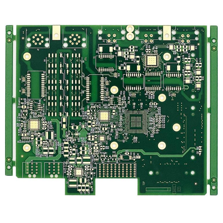
Step-by-Step Process for PCB Assembly Testing and Inspection
You help ensure that every printed circuit board assembly functions properly. Each step in the PCB assembly process requires your close attention. PCB Assembly Tests & inspections are crucial. Careful PCBA testing identifies issues such as flux residues and incorrect component values. If these problems go unnoticed, the product may fail and have a short lifespan.
- Clean inner layers and good solderability enhance the board’s durability.
- Testing how the board performs in real-life scenarios saves customers money.
- Identifying design mistakes early protects your reputation and prevents recalls.
By adhering to each step, every printed circuit board assembly will be of high quality, and you will avoid costly errors.
Key Takeaways
- Check design files carefully before assembly to find mistakes early. This helps save time and stops expensive problems.
- Get parts from trusted suppliers to make sure they are good and real. This keeps your product working well.
- Use different inspection ways, like looking and using machines, to find problems early. This makes the product better.
- Test each part with in-circuit and functional testing to make sure everything works right. This lowers returns and helps customers trust you.
- Always focus on quality at every step. This makes PCBs better and keeps customers happy.
Pre-Assembly Review & DFM Analysis
Before starting the pcb assembly process, you must check your design files. You also need to do DFM analysis. These steps help you find problems early. They make sure your board will work right.
Design File Check
Always look over your design files before pcb assembly. Many mistakes can happen here:
- Design files might be missing or old.
- Assembly drawings may not be complete.
- There could be more than one version of files.
- People might misunderstand the files.
- Components might be in the wrong place.
- Soldering could have mistakes.
If your circuit board documents have errors, you can face big delays. OEMs and pcb assembly engineers might get confused. Skipping this step means your board might not fit your needs.
Tip: Always use the newest design files. Double-check your assembly drawings. This easy step saves time and money.
DFM (Design for Manufacturability)
DFM analysis is very important in pcba manufacturing. You use DFM to spot and fix problems before making the board. This helps you avoid wasting money and materials.
- DFM checks if parts have enough space. This stops short circuits.
- You make sure you use standard part sizes. This keeps things on track.
- DFM looks for soldering problems. You avoid solder bridges and cold joints.
- You balance copper pour to stop heat problems during soldering.
- DFM helps you get more good boards. You have fewer bad ones.
- You make lead times shorter by getting your design ready.
Doing these steps makes your board more reliable. It lowers the chance of defects in your pcba. Careful review and DFM analysis help your pcb assembly go smoothly.
Component Procurement & IQC
Sourcing Components
You need to pick good suppliers for your printed circuit board assembly. Good suppliers help you avoid fake or bad parts. Start by using authorized distributors. These companies show you where the parts come from. They also prove the parts are real. Always check if the supplier is trustworthy. Look for certificates like ISO 9001 or AS9120. Ask for papers that show the parts are tested. These papers prove the parts meet your needs.
Inspect Quality Control Procedures: They must check quality at every step. Ask these questions: Do they check new materials to stop fake parts? Do they use Automated Optical Inspection to find problems? Do they do burn-in tests for long use?
Here are steps to find good suppliers: 1. Read reviews from other companies. 2. Make sure suppliers follow rules like ISO, RoHS, and IPC. 3. Visit their buildings and see how they work. 4. Order a small amount first to check quality. 5. Pick suppliers who talk clearly and honestly.
- Use authorized distributors so you know where parts come from.
- Check if suppliers have the right certificates.
- Ask for papers to prove the parts are real.
Incoming Quality Control
When parts arrive, you must check them before using them. This is called Incoming Quality Control, or IQC. IQC helps you find problems early. You look at each part for damage or missing pins. You also check for fake parts. Use tools like microscopes and X-ray machines to find hidden problems.
You test if the parts work the right way. If you find problems, you send the parts back. Only good parts go to the next step in pcba. IQC keeps bad parts out and makes your boards work well.
PCB Cleaning & Stencil Making
PCB Cleaning Process
You must clean your printed circuit boards before assembly. Cleaning removes unwanted materials that can cause problems later. If you skip this step, your board may not work well. You can use machines or special chemicals to clean the surface. Some companies use ultrasonic cleaners. Others use brushes and water-based solutions. Cleaning helps you avoid short circuits and poor solder joints.
Cleaning is important because it keeps your board safe from damage and defects.
Here are the most common contaminants you need to remove during the cleaning process:
- Ionic contaminants
- Flux residues from soldering
- Etching chemicals
- Moisture
- Inter-layer residues from drilling and via plating processes
You should check the board after cleaning. Use a microscope or magnifier to look for any leftover dirt. If you find any, clean the board again. Clean boards help you get better results in pcba.
Stencil Fabrication for Solder Paste
You need a stencil to apply solder paste to your board. The stencil is a thin sheet with holes that match the pads on your PCB. You place the stencil over the board and spread solder paste across it. The paste goes through the holes and lands on the pads.
Stencil quality affects how well the solder paste is applied. The thickness of the stencil must match the size of your components and pads. If the stencil is too thick, you get too much paste. If it is too thin, you get too little. The shape and size of the holes matter too. Properly sized apertures help you avoid defects. Area ratio and aspect ratio also affect how well the paste releases. Fiducial marks help you align the stencil with the board, which is important for high-density designs.
Tip: Always check your stencil for damage before use. A good stencil helps you avoid soldering problems and makes your assembly process smoother.
Solder Paste & Application Inspection
Solder Paste Printing
You begin by putting solder paste on the pads. This step helps make strong electrical connections. You use a stencil to spread the paste. The paste must cover each pad evenly. If you miss a pad, problems can happen. Using too much paste can also cause damage.
When you do smt first article inspection, you check the first board. You look for even paste and good alignment. The paste should only be on the pads. It should not be between the pads. If you see paste outside the pads, you need to fix it.
Tip: Always check the first board after printing. Finding mistakes early stops them from happening again.
Bad solder paste application can cause many problems:
- Not enough solder makes weak connections. Your PCB might not work right.
- Solder bridging happens when paste joins two pads. This can make short circuits.
- Too much solder paste can cause shorts and other problems. You must avoid this to keep your assembly working well.
Solder Paste Inspection (SPI)
You use solder paste inspection to check the paste after printing. This step helps you find mistakes before adding components. Automated machines measure paste volume, height, area, and alignment. These machines compare results to industry standards.
Here is a table showing common targets for solder paste inspection:
| Inspection Parameter | Typical Process Control Target (IPC-aligned) | Defect (Fail) Threshold |
|---|---|---|
| Paste Volume | 80% – 150% of nominal | < 50% or > 200% |
| Paste Height | ±4 mils (≈±100µm) from nominal | Outside of process window |
| Area Coverage | > 75% | < 50% |
| XY Alignment | < 25% of pad width/misalignment | > 50% of pad width/misalignment |
| Bridging | Zero tolerance | Any detectable bridge |
You do smt first article inspection again after SPI. You check the first board to see if the paste meets these targets. If you find a problem, you fix it before making more boards.
Solder paste inspection helps you avoid expensive fixes and defects. You make sure every board is good before moving to the next step.
Component Mounting in PCB Assembly
SMT (Surface Mount Technology)
You use Surface Mount Technology to place small components on your printed circuit board. This method uses machines called automated pick and place. These machines move quickly and put each part in the right spot. You can mount hundreds of components in just a few minutes.
Component placement accuracy matters a lot in pcba. Even a small mistake can cause big problems. Here is what can happen if you do not place parts correctly:
- Misalignment can cause defects or make the board stop working.
- Placement errors make up about 60% of SMT assembly defects.
- A shift of only 0.1 mm can lead to poor soldering or short circuits.
- If you move a part by 0.05 mm, you increase the chance of soldering problems by 30%.
- In high-speed circuits, a 0.2 mm shift can change signal paths and cause errors.
Tip: Always check the first board after mounting. This helps you catch mistakes early.
You must keep your machines clean and well-calibrated. Good lighting and clear markings on your board help the machines work better. You should also train your team to spot problems fast.
Through-Hole Assembly
You use through-hole assembly for larger parts or connectors. You place each component lead through a hole in the board. Then, you solder the leads on the other side. This method gives strong connections. It works well for parts that face stress or need extra support.
You can use machines or do this step by hand. Hand assembly lets you fix mistakes right away. You should check each part for the right direction and fit. Good through-hole assembly keeps your board strong and reliable.
Note: Use through-hole assembly for connectors, switches, or heavy parts that need to stay in place.
Soldering in Step-by-Step PCB Assembly Process
Soldering joins parts to the board. There are two main ways to do this: reflow soldering and wave soldering. Both ways help make strong connections for your pcba.
Reflow Soldering
Reflow soldering is for surface mount components. First, you put solder paste on the pads. Next, you place the components on the paste. The board goes into a reflow oven. The oven heats the board in steps. The solder melts and makes solid joints.
Reflow soldering lets you control the process well. You can change the temperature and timing for each step. This way works best for small chips and tiny parts. You see fewer problems like tombstoning or bridging. Most factories use machines for reflow soldering.
| Aspect | Reflow Soldering | Wave Soldering |
|---|---|---|
| Best Suited For | SMT components (e.g., fine-pitch ICs) | THT components (e.g., DIP ICs) |
| Process Complexity | Simpler, automated, precise control | More complex, requires expert adjustments |
| Defect Rates | Lower (<1% for tombstoning/bridging) | Higher (2-5% for bridging/solder skips) |
Tip: Always check your oven settings. Good settings melt the solder but do not hurt your parts.
Wave Soldering
Wave soldering is for through-hole components. The board moves over a wave of hot solder. The solder sticks to the leads and pads. This way works well for connectors and big parts.
Wave soldering needs careful setup. You must set the wave height, temperature, and speed. If you set these wrong, you get problems. Common problems are solder bridging, cold joints, and lifted parts.
Here is a table with common soldering problems, why they happen, and how to fix them:
| Defect | Causes | Solutions |
|---|---|---|
| Insufficient Hole Fill | Not enough heat, low wave height, dirty leads | Use more heat, raise wave, clean leads and add flux |
| Solder Bridging | Too much wave, pads too close, uneven flux | Lower wave, change layout, fix flux |
| Cold Solder Joints | Low heat, short time, dirty solder | Watch heat, give more time, change solder or flux |
| Solder Balling | Wet boards, fast wave, not enough flux | Dry boards, slow wave, use more flux |
| Lifted Components | Fast speed, bad placement, heat shock | Slow down, use glue, warm up boards |
Note: You stop most problems by checking your machine and cleaning your boards before soldering.
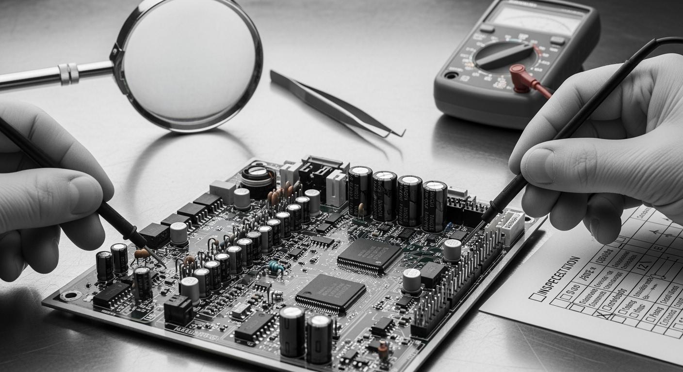
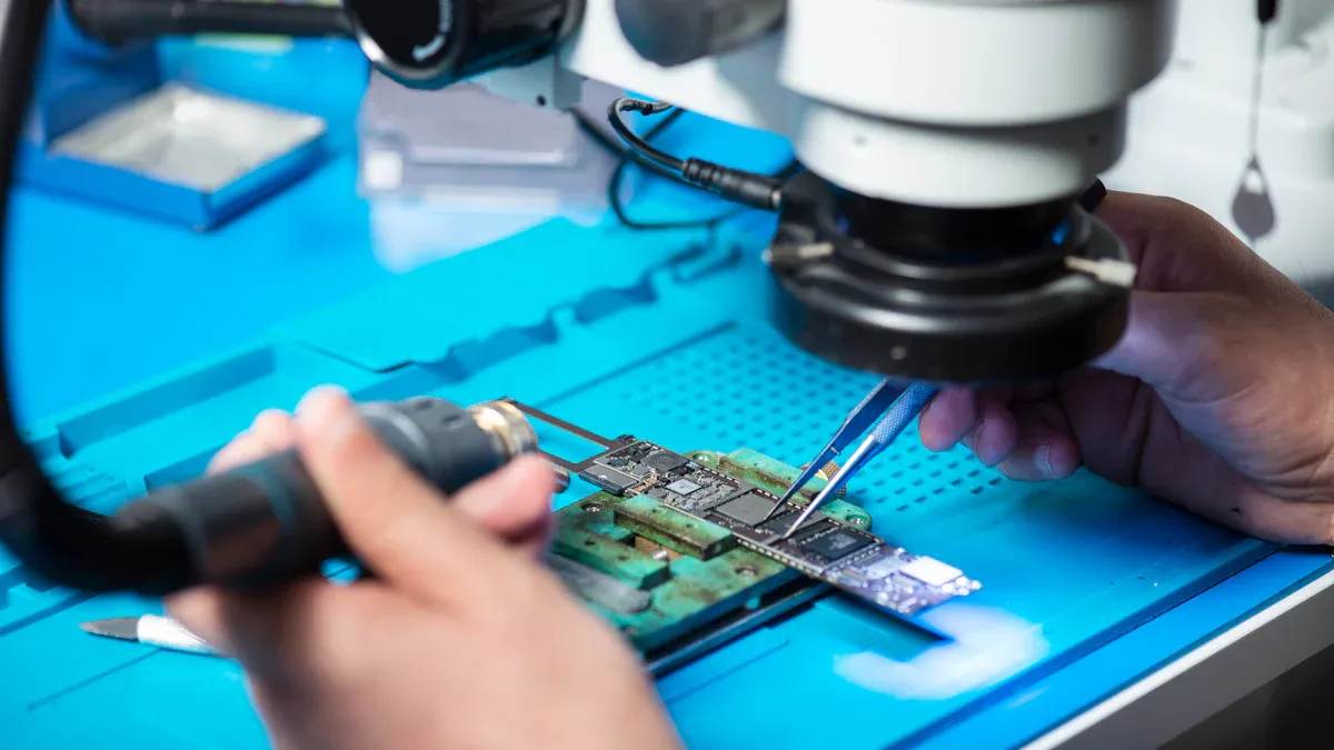
PCB Assembly Tests & Inspections
You must check every board as you build it. These pcb assembly tests & inspections help you spot problems early. You use different test methods to make sure your pcba works well and lasts longer.
Visual Inspection
You begin with visual inspection. You look at the board with your eyes or a magnifier. You check for missing parts and wrong placement. You also look for soldering mistakes. Dirt, scratches, and broken traces are easy to see. Visual inspection is fast and simple. You can find many problems before customers get the board.
Here is a table that shows how well visual inspection works:
| Inspection Method | Defect Detection Rate |
|---|---|
| Automated Visual Inspection | 99.5% |
| Manual Inspection | 85% |
Automated inspection finds almost all defects. Manual inspection still catches most problems. You might miss some if you only use your eyes. Using both methods gives you the best results.
Tip: Always check the first board after assembly. Early tests help you stop mistakes from spreading.
Automated Optical Inspection (AOI)
You use automated optical inspection to check boards faster and better. AOI uses cameras and computers to scan each board. You find tiny problems that people might miss. AOI works much faster than manual inspection.
- AOI checks PCBs over 80 times faster than manual ways.
- AOI finds 25% more defects than manual inspection.
- False defect rates drop from 0.5% to 0.02%.
You can use in-line automated optical inspection during pcb assembly. This test checks every board as it moves down the line. You also use offline automated optic inspection for boards that need extra care. AOI finds many types of defects:
- Dimensional errors like wrong pad sizes or trace widths.
- Surface defects such as warping, dirt, or scratches.
- Component issues like wrong polarity or misalignment.
- Soldering problems such as cold joints or solder bridges.
You use in-line automated optical inspection for quick checks. You use offline automated optic inspection for detailed tests. AOI helps you catch problems early and improve your pcb assembly tests & inspections.
Note: AOI does not replace human checks. You should use both automated and manual tests for the best results.
X-ray Inspection
You use X-ray inspection for boards with hidden parts. Some defects hide under chips or inside layers. X-ray lets you see inside the board. You find problems that other tests miss.
Here is a table that shows what X-ray inspection finds best:
| Defect Type | Description |
|---|---|
| Solder Voids | Tiny gas bubbles in solder joints that weaken strength and conductivity. |
| Solder Bridges | Accidental connections between adjacent pins or pads that can cause short circuits. |
| Insufficient or Excess Solder | Too little solder risks weak joints; too much can cause shorts. |
| Misaligned Components | Misplaced parts that disrupt connections, especially in dense boards. |
| Internal Cracks and Delamination | Flaws in vias or between layers that threaten PCB structure and signals. |
You use X-ray tests for boards with ball grid arrays or fine-pitch chips. You also use X-ray for boards with many layers. X-ray inspection is part of your pcb assembly tests & inspections. You use offline automated optic inspection to review X-ray images and find hidden problems.
Tip: Use X-ray inspection for boards with hidden solder joints. This test helps you find problems that other methods miss.
You need to use many test methods during the pcb assembly process. You use visual inspection, in-line automated optical inspection, offline automated optic inspection, and X-ray inspection. These pcb assembly tests & inspections help you deliver strong and reliable boards.
PCBA Testing Methods
You need strong pcba testing to make sure your boards work well. You use different testing methods to check every part and every function. Two main types help you find problems early and keep your products reliable. These are in-circuit test and functional test.
In-Circuit Testing (ICT)
You use in-circuit test to check each component on your board. This testing method uses a fixture with many tiny probes. The probes touch test points on your pcba. You measure resistance, capacitance, and other values. You find open circuits, short circuits, and wrong parts. In-circuit testing helps you catch problems before you finish assembly.
Here is a table showing what in-circuit test checks:
| Test Type | What It Finds | Why It Matters |
|---|---|---|
| Open Circuit | Broken connections | Stops board failure |
| Short Circuit | Unwanted connections | Prevents damage |
| Wrong Component | Incorrect parts | Ensures right function |
| Solder Defect | Bad joints | Improves reliability |
You use in-circuit testing methods for fast and accurate results. You can test hundreds of boards in a short time. You do not need to power up the board for this electrical test. In-circuit testing gives you confidence that your pcba has no hidden defects.
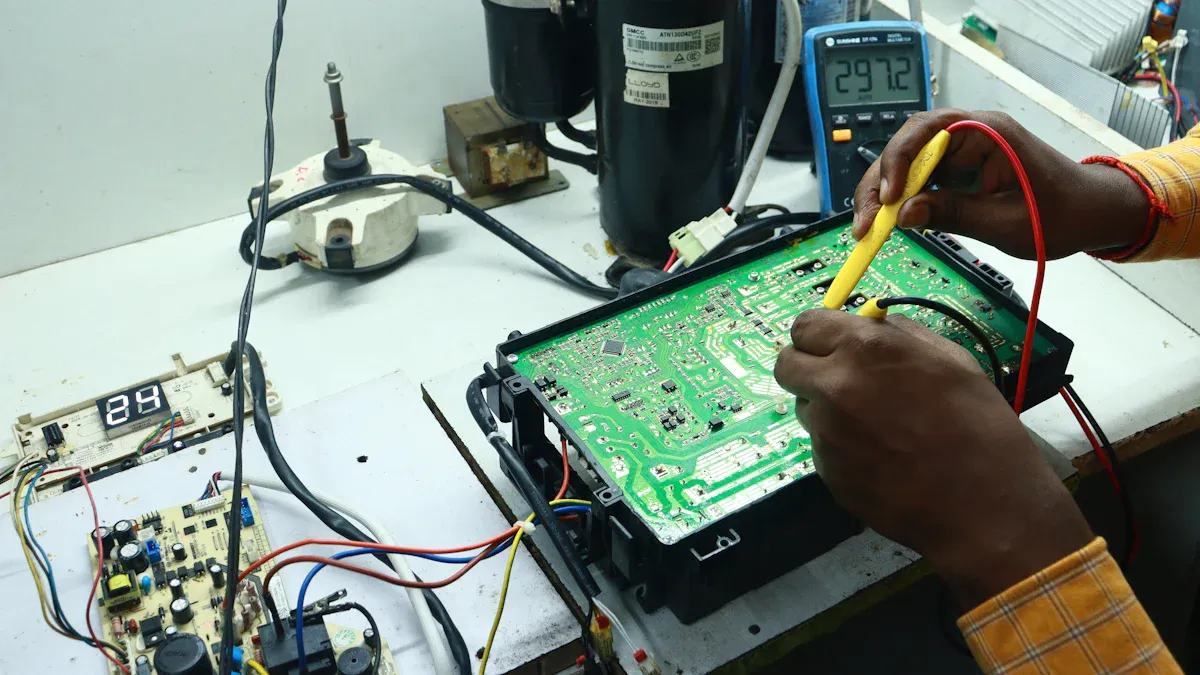
Functional Circuit Testing (FCT)
You use functional test to see if your board works as designed. This testing method powers up the pcba and runs it like it would work in real life. You check if signals move the right way. You test buttons, displays, and outputs. Functional testing shows if your board meets all design needs.
Functional circuit testing gives you many benefits:
- You deliver only high-quality boards to your customers.
- You find defects that other tests may miss.
- You meet strict safety and performance rules.
- You check if your board works under real-world conditions.
- You confirm every component does its job.
- You make sure your board matches design specifications.
- You build trust with customers by reducing returns and complaints.
Functional test helps you avoid costly rework and product recalls. You use functional testing methods to make sure your pcba works every time. You can use automated systems to run these tests quickly. You keep your products safe and reliable with strong pcba testing.
Tip: Always use both in-circuit test and functional test for complete pcba testing. You find more problems and deliver better boards.
Final Quality Control & Shipment
Final Cleaning & Conformal Coating
You begin by cleaning your pcba. Cleaning takes away dust and leftover flux. This step helps stop electrical shorts. It also keeps your board looking nice. After cleaning, you put on conformal coating. This is a thin layer that covers your board. The coating protects against water, dust, and chemicals. It blocks humidity and stops current from leaking. This helps prevent corrosion and shorts. Your board stays strong even in tough places. You lower the chance of problems and returns. Your board can work in many places and saves users money over time.
Tip: Always look at the coating to make sure it covers everything. If you miss a spot, the board could get damaged during shipping.
Quality Assurance Checks
You need to test your board before sending it out. These tests make sure your board is built right. You use visual inspection, automated optical inspection, X-ray inspection, in-circuit testing, and functional testing. Each test looks for different problems. This helps you send out good boards.
| Inspection Method | Description |
|---|---|
| Visual Inspection | Inspectors look for problems on the surface and underneath using special tools. |
| Automated Optical Inspection (AOI) | Cameras check for missing parts and parts in the wrong place. |
| X-Ray Inspection | Finds hidden problems under parts or between layers that can hurt the board. |
| In-Circuit Testing (ICT) | Checks if parts are working and if the circuit is complete. |
| Functional Testing | Makes sure the board works as it should for its job. |
You do these checks to find any last problems. You make sure your board passes every test. Boards that go through final checks have fewer problems. The reject rate is about 900 PPM with checks, but 5500 PPM without them. Your customers get boards they can trust.
Packaging & Pre-Shipment Inspection
You keep your board safe during shipping with special packaging. You use ESD bags and foam to stop static damage. You put boards in strong boxes with foam or bubble wrap. You add bags and packets to keep out water. Sometimes you use custom boxes or crates for special orders. You make sure the board cannot move and is safe from bumps.
Note: Always check the packaging before you ship. Good packaging keeps your board safe from harm.
You do one last check before shipping. You look for missing labels, broken boxes, and the right papers. You make sure every board meets your quality rules. You want your customer to get a perfect board.
You finish the last checks and tests to make sure your board is reliable. You follow every step to send out high-quality pcba assemblies every time.
You make products work better and keep customers happy by doing every step in PCB assembly tests and inspections. Good pcba testing helps you find problems early. This means fewer returns and more trust from customers.
- You save money because you stop problems before they happen.
- You follow rules and give people safe products.
| Certification | Description |
|---|---|
| IPC | Tells how to build PCB assemblies the right way. |
| ISO | Helps companies do better work and be more organized. |
| RoHS | Keeps people safe by not allowing dangerous materials. |
Always focus on quality assurance. Use smart ways and good inspection tools to make sure every board is great.
FAQ
What is the difference between visual inspection and AOI?
Visual inspection means you look at boards with your eyes or a magnifier. AOI uses cameras and computers to check for problems. AOI finds defects faster and more accurately than people can.
Why do you need X-ray inspection in PCB assembly?
X-ray inspection helps you find hidden problems under chips or inside layers. It lets you see solder joints and connections that other tests cannot reach. This way, you catch issues you might miss otherwise.
How does functional testing improve pcba reliability?
Functional testing checks if your board works the way it should. It helps you find problems that other tests do not catch. Reliable boards mean fewer returns and happier customers.
What packaging protects PCBs during shipment?
You use ESD bags, foam, and strong boxes to keep boards safe. These protect your PCB from static, moisture, and bumps. Good packaging makes sure your board arrives safely.
When should you apply conformal coating?
You put on conformal coating after you clean the board. This thin layer keeps water, dust, and chemicals away. It helps your PCB last longer in tough places.