 English
 Arabic
 Chinese (Simplified)
 Dutch
Dutch French
 German
 Italian
 Portuguese
 Russian
 Spanish

You have a PCBA prototype that works. Now you need to turn it into a full box-build product ready for the market. This jump requires a clear, planned approach. You must focus on manufacturability, scalability, and quality. A weak plan leads to costly delays and a failed product launch. Your goal is simple: move from pcba prototyping to box-build production without surprises. Treat this transition as a roadmap. Each phase builds on the last one. You start with a solid design. Then you refine your processes. Finally, you scale up with confidence. With careful planning, you can achieve a smooth and successful manufacturing launch.
Key Takeaways
Lock in your BOM early to set part numbers and prevent delays in production.
Do DFM and DFA reviews to find design problems before manufacturing.
Make a test plan that can grow with your project, and use automatic checks to make sure everything works well.
Run a test batch to find problems before you start full production.
Pick a turnkey manufacturer for a smooth move to box build.
From PCBA Prototyping to Production
Your working prototype shows the design is good. Now you must turn it into a build that is ready for production. The first step is going from a prototype BOM to a production BOM. A prototype BOM often has parts picked for ease, not for large amounts. Your prototype assembly may use a hand-soldered substitute or a part a distributor had in stock that week. A production BOM locks every part number, package, and approved alternate. This lock keeps your pcba manufacturing line steady and repeatable.
Finalizing the Bill of Materials
A finalized BOM boosts yield and controls cost. You should cut the number of unique components. Fewer unique parts make inventory, storage, and supply-chain work simpler, which directly lowers BOM cost. You should also stay away from single-source-only parts. Approved alternates keep supplier choices open and stop price spikes from low stock or long lead times. Making the PCB itself simpler, like fewer layers or a cheaper surface finish, can raise PCB yield and push down overall cost. Locking the BOM with lifecycle checks stops last-minute substitutions and keeps assembly steady. Standardizing solder paste, stencil thicknesses, and reflow profiles cuts changeover time and scrap, which improves first-pass yield.
Scrubbing the BOM for Availability
Scrubbing the BOM means checking every line for lifecycle status, availability, and cost at volume. Component obsolescence is a constant threat to your schedule.
Fifteen percent of electronic parts disappear from the market annually.
That rate makes end-of-life and not-recommended-for-new-design parts a real risk. Common BOM errors cause most delays. Review this table before you release the build.
BOM error | How it delays production |
|---|---|
Missing components | Assembly cannot proceed when parts are omitted. |
Missing manufacturer part numbers | Procurement stalls on incomplete part data. |
Obsolete components | End-of-life parts force redesign or substitution. |
Missing alternate parts | Sourcing flexibility drops when primary parts run out. |
Footprint or package mismatches | Wrong package data leads to assembly failures. |
Duplicate BOM entries | Over-ordering creates inventory inaccuracies. |
Quantity mistakes | Shortages stall production; excess stock wastes money. |
Outdated BOM shared with the contract manufacturer | A stale BOM creates mistakes and launch delays. |
This scrub protects your box-build schedule and your budget. It also keeps your prototyping lessons intact as you scale.
The PCB-to-Box-Build Handoff
This is the critical handoff. You shift from prototype assembly thinking to a manufacturing process. Your PCBA prototype proved the circuit works. Now you must prove the product builds at scale. The PCB-to-box-build handoff turns your working board into a repeatable system. Every choice here affects yield, cost, and schedule.
Conducting a DFM and DFA Review
For your PCBA, a DFM and DFA review is essential. DFM checks the design for manufacturability. DFA checks the design for assembly. Together, they catch problems early.
Start by gathering review inputs. Collect fab notes, assembly notes, stack-up data, paste layer, 3D STEP files, enclosure CAD, test plans, and BOM with alternates. Missing inputs delay sign-off.
Then run focused review passes. Check layout, land patterns, stencil, paste, panel, fiducials, test access, mechanical fit, fasteners, and safety marks. Pick a lead reviewer plus domain reviewers for layout, mechanical, test, and quality. Log every action item.
Document deviation evidence. If you break a rule, such as tight RF clearance, attach reason and validation data. Production teams must not guess. Enforce sign-off gates. Make DFM approval a release criterion equal to schematic and layout approval.
Work with your contract manufacturer early. Share early Gerbers, 3D CAD, and a preliminary BOM. Request their standard rules and stencil preferences. Make build intent clear. Say whether the run is EVT, DVT, PVT, or mass production. Control changes with an ECO process. Supply golden samples for AOI programming. These actions prevent unapproved substitutions and unclear test steps.
The business case is strong. Assembly operations use 40–60% of total costs. Well-run DFA projects show a 10:1 ROI or more. DFM optimization cuts product costs by 10–25%. Rework and defect costs drop by 5–15%. At ITT Aerospace, a documented DFA review cut total product cost by 24%.
Use phase-appropriate rigor. At EVT, accept hand rework but keep a minimum DFM bar. At DVT, run full DFM and add ICT pads. At PVT, freeze panels, labels, packing, and fixtures. Track yield across lots.
Optimizing PCB Panelization
Panelizing the PCB helps make assembly efficient. You run solder paste, placement, and reflow once for each panel. This cuts cycle time and boosts SMT line capacity. A standard panel shortens setup. Pick-and-place machines stay busy longer.
Panelization also cuts down waste. Better board nesting wastes less laminate. Standard panels lower storage, packing, and shipping costs. Rigid panels stop small boards from warping during reflow. Automated printers and reflow ovens can handle small or irregular boards.
Ask your manufacturer about the maximum PCB size they can handle. Build your panel layout around that limit. Use standard rails with tooling holes and global fiducials. Specify mouse-bites or V-score with sensitive edges protected. Place barcodes for AOI visibility.
These tweaks matter for box-build assembly. They decide how well boards move into enclosure integration. Good panels keep your PCB assembly line running well. They also let your box build partner focus on wiring, fasteners, and final test.
For PCB box-build assembly, the handoff review is your safety net. It catches design errors, missing parts, and manual assembly risks before they grow. A strong PCB box-build plan checks wiring, labeling, and final test. The real question is whether you catch them now or at scale.
Developing a Scalable Test Strategy
Prototype testing often means manual checks, a bench multimeter, and starting firmware from a laptop. That works for one board, but not for many. A production line cannot depend on manual inspection. You need a test plan that grows, built on automated inspection and organized checks.
Moving Beyond Prototype Testing
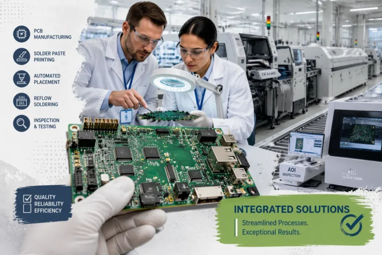
You add automated checks in layers. Common pcba test methods include AOI for solder look, X-ray for hidden joints, ICT for node checks, flying probe for low volume, and functional testing for powered use. The table below sums up the trade-offs.
Method | What it verifies | Typical limitation |
|---|---|---|
AOI | Visual placement and solder appearance | Cannot see hidden joints or powered operation |
X-Ray | Internal solder joints, such as BGA/QFN bridges, opens, and voids | Does not prove electrical function |
ICT | Electrical checks on accessible nodes and components | Requires fixture access; limited system/firmware coverage |
Flying Probe | Fixtureless electrical checks for prototypes and low volume | Slower at volume; limited full-board operation |
FCT | Powered board-level operation, including power, I/O, firmware, and alarms | May need structural testing to localize faults |
Test escapes still happen, and they cost real money. Return material authorizations can cost semiconductor companies hundreds of thousands to millions of dollars each year. Escapes also cause lost sales, harmed customer ties, and bad contract terms. In a customer study, almost one-third of failed devices were No Fault Found—the problem could not be repeated. The other two-thirds traced to process escapes or faulty parts. Automated algorithmic rules can cut RMAs by 50% with little impact on yield or test time. That drop protects your margin when a tested pcba moves into the final box-build assembly.
Designing for Testability
Design your board for testability before you finish the layout. Add test points on reachable nodes. Avoid hiding signals under BGAs. Include firmware commands that work power rails, I/O, and alarms. Define test criteria once you know the failure modes you must catch. Those criteria guide fixture design and test software.
A test jig holds the board, touches test points, and runs a scripted sequence. Build jigs for thousands of cycles. Design them for quick loading and clear pass/fail signs. When you design for test early, you cut fixture cost and cycle time. You also give your manufacturing partner a repeatable process. The result is a stable assembly line and a reliable full box-build product.
The Importance of a Pilot Production Run
A pilot run is a small batch that acts like full-scale manufacturing. You make a limited amount using the same tools and suppliers you plan to use for volume. This run checks assembly, yield, and test coverage with real data. The pilot run is a key way to lower risk.
Validating the Assembly Process
Run pilot programs at a medium volume. Hundreds to thousands of units meet early demand while bringing problems to the surface. Checking about 10 units for defects catches issues that low-volume prototyping misses.
Mechanical and thermal testing show environmental weak spots. Do shock testing on early units. Run burn-in or accelerated life testing on about 10 units. These tests reveal early failures before your box-build line ramps up. The pilot run also checks your pcba design under real assembly line conditions.
A readiness review adds one more layer. Look at assembly complexity, component access, tolerances, and thermal concerns. Check your BOM for critical component availability. Ask about long lead times. Look for single-source components that are near obsolescence. Qualified suppliers keep your schedule on track.
Uncovering Hidden Issues
Pilot runs bring out problems that design reviews miss. A critical component may show a long lead time before launch. A connector might become hard to reach during testing. The assembly may need a slow manual adjustment. These reveal hidden supply chain and assembly gaps.
Common issues follow patterns you can predict. A design may pass prototype builds but fail under automated pick-and-place. Tight component spacing causes solder bridges or tombstoning. Catalog parts may turn out to be near end-of-life. One voltage regulator had a 52-week lead time in a past program.
Documentation gaps also show up here. Assembly knowledge kept only in an engineer’s head does not pass to your EMS partner. Missing work instructions and quality criteria cause yield loss. Operators start guessing at unclear steps.
Find the root cause of each failure in a controlled way. Have engineering and manufacturer quality teams check failing units. Send those findings back to engineering with clear fixes. Apply fixes before scaling to full-rate output. This loop turns pilot findings into a stronger tested pcba. Your final box-build product then meets quality targets with fewer surprises.
Getting Certifications for Box Build Assembly
A bare pcba does not need the same approvals as a finished product. Once you put that board inside an enclosure with wiring, a power supply, and connectors, the whole unit becomes the “box.” Regulators now check the whole product, not just the circuit. This change affects which certifications you need, your budget, and your launch schedule. You must plan for this during box-build assembly, not later.
Finding Required Certifications
Which marks you need depends on your market. Start with the region where you plan to sell it.
Region | Required Certifications |
|---|---|
United States | FCC (mandatory), UL, CSA, IEC/EN standards |
European Union | CE (mandatory), WEEE, RoHS |
For electronics sold in the United States, the FCC is required. It limits electromagnetic interference. UL is optional but well trusted, and it covers fire and electric shock risks. Across the European Economic Area, CE marking is required. It shows the product meets EU safety, health, and environmental rules. WEEE and RoHS also apply in the EU.
Getting Ready for Compliance Testing
Testing cost and time vary by product type. A simple SDoC device costs $2,000–$5,000 and takes 2–4 weeks. A wireless product with a certified module is $7,000–$12,000 and needs 4–8 weeks. For a custom RF or multi-radio device, expect $15,000–$40,000+ and 8–16 weeks. A cellular or complex connected device can cost $40,000–$100,000+ and take 3–6 months.
The enclosure is a big cost factor. Conductive or non-conductive materials, vent holes, and cable openings all affect shielding. Use the near-final enclosure in final tests, since enclosure changes alter emissions. A revision can cost thousands of dollars and add weeks.
Get your documents ready early. Collect schematics, BOMs, block diagrams, and user manuals. Send pre-production samples matching the final build. This keeps your pcb box-build assembly schedule on track. It also protects your manufacturing budget from surprise retests.
Selecting PCB Box Build Assembly Services
Picking the right contract manufacturer really matters. Your partner affects your yield, your timeline, and how people see you. Box build assembly means putting together the whole final electronic product. It covers pcb assembly, internal wiring, and fitting everything into an enclosure. A good partner can do all of this in one place.
What to Look for in a Partner
To pick a manufacturer for box build assembly, look at their turnkey electronics integration skills and their experience with full box build production. Look for these traits:
Certifications that fit your program. Ask for current certificates showing scope and expiry dates. Check them with the certifying body.
Experience across the whole path from quick-turn pcba prototyping to mass production. Changing suppliers between phases resets proven process baselines.
Turnkey abilities. A turnkey pcba manufacturer handles design, sourcing, testing, and delivery. This cuts down handoffs and supply-chain complexity.
Clear communication. Ask who your main program contact is and how often they will update you during active builds.
A turnkey pcb box build assembly service also handles enclosure sourcing, mechanical design, and first-article inspection. Make sure mechanical work happens in the same workflow as pcb assembly and test. Ask how they handle component end-of-life events and how many approved alternates exist for each critical component family. These answers show whether they think past the current build.
Ensuring a Smooth Transition
Treat your prototype as a sample, not as an undocumented build instruction. Fix any mismatch between the sample and the controlled files. Release controlled documents that can travel without the original designer. This includes fabrication data, assembly info, BOM, enclosure drawings, and programming references. Remove vague notes like “adjust as needed.”
Run a cross-functional readiness review with engineering, quality, purchasing, and your manufacturing partner. Give every open item an owner and a decision. Check the supply plan against the actual production BOM. Make clear who approves material purchase versus assembly. Replace bench success with a usable acceptance process. Define conditions, limits, approved software, and result records.
Show that assembly and delivery are ready. Check connector access, cable routing, fastener installation, enclosure tolerances, labeling, accessories, and packaging. Use a controlled pilot to close remaining open questions before full production. This step protects your box-build schedule and your budget.
You began with a pcba that worked. Now you have a product ready for the market. This trip takes self-control. Finish your BOM. Do DFM and DFA reviews. Create a test plan that can grow. Check everything with a pilot run. Every step guards your budget.
Think of your manufacturer as a partner, not just a seller. A strong partnership brings faster product launches, better quality control, and lower total cost of ownership. You get less supply chain hassle and more operational visibility. These gains build up with every production cycle.
Plan for the next stage of your product’s life. Your pcb box-build assembly partner can help you grow. A smooth transition sets up your next pcb box-build assembly win.
FAQ
How long does it take to go from PCBA prototype to full box build?
The time depends on how complex your product is and where you sell it. A simple device with a self-declaration of conformity may need only a few weeks of compliance testing. A wireless or multi-radio product takes longer. Plan your schedule around BOM scrubbing, DFM review, a pilot run, and certification. Then add extra time for retests.
What is the biggest risk during this transition?
Component obsolescence is at the top of the list. About fifteen percent of electronic parts leave the market each year. An end-of-life part forces a redesign or a swap late in the program. Check your BOM for lifecycle status and approved alternates before you release the build. This one step stops most schedule slips.
Do I need new certifications for the finished box?
Yes. A bare PCBA does not carry the same approvals as a finished unit. Once you add an enclosure, wiring, and a power supply, regulators check the whole product. The FCC is required in the United States. CE marking is required in the European Union, and WEEE and RoHS also apply there.
How many units should a pilot run include?
A pilot run uses the same tools and suppliers you plan for volume. Hundreds to thousands of units meet early demand while bringing problems to light. Inspect about ten units for defects, and run burn-in or accelerated life testing on roughly ten more. This sample size shows issues that low-volume prototyping misses.
Can one manufacturer handle both PCBA and box build?
Yes, and a turnkey partner makes the handoff easier. Look for a manufacturer with experience across the full path from quick-turn prototyping to mass production. Make sure they handle enclosure sourcing, mechanical design, wiring, and final test in one workflow. Ask how they manage component end-of-life events and approved alternates.