Comprehensive Guide to PCB Design Steps

Printed circuit boards (PCBs) are the base of modern gadgets. Almost every device, like phones or medical tools, needs a good PCB design. This design helps parts work together perfectly for the best results.
Designing a circuit board is more than placing parts. It turns ideas into working products that can be made easily. By being careful and efficient, you can make designs that work well and are easy to produce.
A good PCB design connects new ideas to real-life use, making electronics dependable and easy to grow.
Key Takeaways
- PCB design is important to make devices safe and work well. Knowing this helps create more reliable products.
- Planning carefully during the first steps saves time and avoids mistakes. Pay attention to heat control and picking the right materials.
- Picking good PCB design software is very important. Choose tools that fit your skills and project to work better.
- Checking design rules (DRC) and electrical rules (ERC) finds errors early. This step makes your PCB better and more dependable.
- Clear files, like Gerber files and a Bill of Materials (BOM), are needed for easy production. These help manufacturers understand your design correctly.
Overview of PCB Design
What is PCB Design?
PCB design means planning how a circuit board looks and works. It connects parts using metal paths and pads on a non-metal base. Special software helps make sure the board fits electrical and physical needs. The goal is to make a board that works well and fits into devices easily.
Why PCB Design Matters
PCB design is very important for modern gadgets. It makes sure devices work safely and correctly. For example, in hospitals, PCBs run tools like patient monitors, where accuracy is key. In cars, they help systems like electric engines work smoothly. Below is a table showing how PCBs are used in different fields:
| Industry | How PCBs Help |
|---|---|
| Factory Electronics | Improve machines, controls, and automation for better reliability and speed. |
| Healthcare | Run medical tools, ensuring safe and accurate monitoring for patients. |
| Space and Aviation | Support navigation and flight systems in tough conditions. |
| Cars | Help advanced driving systems and electric car parts work well. |
| Computers and Phones | Make networks faster and more reliable for sharing data. |
| Everyday Gadgets | Allow smaller designs and better features in phones and laptops. |
PCB designs have improved over time to fix problems like weak connections. For example, flexible designs are better for tough jobs like in planes or military tools.
Goals of PCB Design
PCB design aims to make boards work well and easy to build. You need to think about size, materials, and layers. For example, matching board size to machine limits saves money. Using common materials makes production faster. One study showed that changing pad spacing on a board cut failures from 10% to 1%. This proves good design helps production.
Other goals include keeping the right thickness for strong holes and using proper trace widths for better electricity flow. By focusing on these, you can make boards that meet both technical needs and are easy to produce.
Preparation Steps
Requirement Analysis for Circuit Board Design
Before designing a PCB, you must study its needs carefully. This step ensures the board works well and can be made easily. Start by figuring out what the board will do and where it will be used. For instance, a medical device board must be reliable and precise. A board for gadgets might focus on being cheap and small.
Checking how heat spreads is very important here. It helps you make sure the board stays reliable. Decisions like picking the right material, planning the PCB stackup (layer arrangement), and placing parts depend on this step. Good heat management improves how long the board lasts and how well it works.
Tip: Clear planning now saves time and avoids mistakes later.
Component Selection and Library Management
Picking the right parts is key to a good PCB. Even small errors in part details can cause big problems. Choose parts that match your design’s needs for power and size. Avoid outdated parts by checking if they are still in use. This keeps your design current and useful.
Keeping your part library organized is also important. Using old designs can save time and keep data accurate. Tools like Altium’s library system help manage growing libraries without slowing work. Quickly finding where parts are used makes updates easier and keeps designs correct.
Note: Grouping similar parts together makes building and wiring simpler.
Choosing PCB Design Software
Picking the right PCB software is an important step. The software should match your project needs and skill level. Popular choices include Altium Designer, Fusion, and PADS Professional. Each has special features for different industries.
| Software Package | Satisfaction Rating | Ease of Use Rating | Quality of Support Rating | Industry Segment Served |
|---|---|---|---|---|
| Altium Designer | High | Below Average | Excellent | Small Businesses |
| Fusion | High | Below Average | Excellent | Small Businesses |
| PADS Professional | High | Below Average | Excellent | Small Businesses |
When choosing software, think about how easy it is to use, the support offered, and if it fits your goals. Beginners should pick tools that are simple to learn. Experts might look for advanced features like signal checks and 3D views.
Tip: Try different software to find the one that works best for you.
Schematic Design and Capture

Circuit Schematic Creation
Making a schematic is the first step in designing a PCB. A schematic is like a map showing how parts connect to work together. Use your design software to place parts like resistors, capacitors, and chips. Label each part with a unique name, like R1 or C1, to keep things clear.
To make it easy to read, use a grid to align parts neatly. Add notes to explain tricky sections. For big projects, split the schematic into smaller diagrams to show how signals flow. Include a title block with the circuit’s name and version for proper records.
Tip: Check your schematic carefully before starting the layout. This avoids mistakes and saves time later.
Linking Components to Footprints
After finishing the schematic, match each part to its footprint. A footprint shows the size and shape of a part on the board, including its pins. Most design tools have ready-made footprints, but you can create your own if needed.
Correct footprints are important to ensure parts fit during production. Wrong footprints can cause assembly problems or failures. Use standard symbols and follow IEEE rules for consistency. Also, check that footprints match the Bill of Materials (BOM) details.
Note: Always double-check pin connections between the schematic and footprint to avoid errors.
Electrical Rule Check (ERC)
The Electrical Rule Check (ERC) finds mistakes in your schematic automatically. It checks if connections follow design rules, like correct voltage levels and proper net links. ERC tools can spot problems like unconnected pins or short circuits.
You can adjust ERC settings to fit your design needs. For example, set rules to keep safe distances between electrical parts. This step improves signal quality and ensures the design meets manufacturing standards.
Key Benefits of ERC:
- Finds mistakes early, preventing design problems.
- Makes the final PCB more reliable.
- Speeds up the process by catching errors automatically.
Using ERC helps save time and makes your design better. Fix all issues before moving to the layout stage.
PCB Layout Design
PCB Stackup and Layer Configuration
The stackup shows how layers in a PCB are arranged. It affects signal quality, heat control, and how easy it is to make. Plan the layers carefully to meet your board’s needs. For fast signals, impedance control is very important. It helps signals move smoothly without losing power. Reducing crosstalk is also key. Arrange signal layers and ground planes to block interference.
Simulations can predict problems like signal delays before making the board. These tests help improve the stackup for better performance. Using thermal vias (holes filled with metal) helps manage heat. This makes devices last longer and work better.
Tip: Keep layers balanced and symmetrical to avoid bending during production.
Component Placement Techniques
Placing parts correctly makes the PCB work well and easy to build. Group parts by their job. For example, put power parts near the power source. Place signal parts close together to shorten paths and improve signals.
Crowded designs need special tricks. HDI designs use thin layers and tiny vias to fit more parts. BGA breakout methods help connect tightly packed parts. Automated tools follow rules to place parts quickly and correctly. These tools save time and reduce mistakes.
| Aspect | Description |
|---|---|
| HDI PCB Stackup Design | Uses thin layers to fit more parts in small spaces. |
| Microvia Structures | Tiny holes connect layers for denser layouts. |
| BGA Breakout Techniques | Routes traces for Ball Grid Array parts in tight spaces. |
Note: Keep fragile parts away from hot areas to avoid damage.
Routing Strategies for PCB Design
Routing connects parts with paths that carry electricity. Start with important signals, like fast or paired ones, before simpler paths. Use short, direct routes to improve performance and lower resistance.
For boards with many layers, use some layers for power and ground. This reduces noise and keeps signals steady. Avoid sharp turns in paths, as they can cause problems. Use smooth curves or angled bends instead. Routing tools in design software make this easier by following spacing and width rules.
Tip: Follow trace width and spacing rules to meet production needs.
Design Rules and Constraints
Design rules and constraints are the main guides for making a good PCB layout. They help you design a board that works well, meets safety needs, and is easy to build. Following these rules ensures your PCB is reliable and simple to produce.
Why Design Rules Matter
Design rules are like a checklist for your PCB layout. They help avoid problems like signal noise, overheating, or building errors. For instance, using the right trace width stops overheating by handling current properly. Spacing rules prevent sparks and make the board safer. Without these rules, your PCB might break or cost too much to make.
Key Types of Constraints
There are different types of constraints to think about when designing a PCB. Each type focuses on a specific need for performance or production. The table below shows the main constraints and how they affect PCB design:
| Constraint Type | Key Points |
|---|---|
| Electrical Constraints | – Impedance Control: Keeps signals clear and steady. |
| – Via Types and Sizes: Affects signal flow and power. | |
| – Maximum Trace Length: Stops signals from weakening. | |
| – Pin Delay: Important for timing in fast circuits. | |
| – EMC/EMI Considerations: Reduces signal interference. | |
| – Stitching Vias: Improves grounding and lowers EMI. | |
| – Allowed Routing Layers: Controls signal quality and noise. | |
| Physical Constraints | – Trace Width: Handles current and keeps signals strong. |
| – Differential Pair Routing: Needs special rules for signal quality. | |
| – Component Placement: Affects signal flow and heat control. | |
| – Board Outline and Dimensions: Set by size limits. | |
| Spacing Constraints | – ESD Protection: Keeps parts safe from electric shocks. |
| – EMI/Crosstalk Mitigation: Proper spacing avoids signal mixing. | |
| – Clearance Rules: Sets minimum space between parts. | |
| – Creepage and Clearance: Stops sparks between parts. | |
| Manufacturing Constraints | – Fabrication Rules: Makes production easier and cheaper. |
| – Assembly Rules: Guides part placement and soldering. | |
| – Test Rules: Sets up testing needs for the board. | |
| – Annular Ring: Minimum copper width around drilled holes. | |
| – Hole Sizes: Must fit the parts used. |
Applying Constraints in Your PCB Layout Design
When starting your PCB layout, set these rules in your design software. Most tools let you adjust trace width, spacing, and via sizes. For example, if your board has fast signals, you can set impedance rules to keep signals steady. You can also set spacing rules to keep parts and traces far enough apart.
Placing parts correctly is also important. Group related parts together to shorten paths and improve signals. For example, place decoupling capacitors near power pins to reduce noise. Use the board outline to set the size of your PCB so it fits inside the device.
Balancing Performance and Manufacturability
While following design rules, think about how easy it is to make the board. Complicated designs can cost more and take longer to produce. For example, using too many layers or odd hole sizes can make production harder. Work with your PCB maker to know their limits and adjust your design.
Tip: Use design rule checks (DRC) in your software often to find mistakes early. This saves time and avoids problems during production.
By applying design rules and constraints carefully, you can create a PCB that works well, lasts long, and is cost-friendly.
Verification and Error Correction
To make sure your PCB works properly, you need to check it carefully. This step finds and fixes problems before making the board. Doing this saves time, lowers costs, and makes your board more reliable.
Design Rule Check (DRC) for Printed Circuit Board
The Design Rule Check (DRC) is an important part of checking your PCB. It ensures your design follows rules like trace width, spacing, and clearance. These rules help avoid problems during production and improve how the board works.
- DRC checks your layout to meet design rules.
- It finds mistakes like overlapping paths or small gaps that cause issues.
- Running DRC reduces the need for multiple prototypes, saving money.
- It helps use board space better by placing parts efficiently.
- DRC ensures your design matches what your manufacturer can build.
- It keeps signals clear by keeping enough space between copper parts.
Tip: Always run a DRC before finishing your design. This avoids costly mistakes later.
Signal Integrity and Power Analysis
Checking signal integrity and power is key to making your PCB work well. Bad signals can cause errors and failures. Power analysis ensures all parts get steady power.
Key Parts of Signal Integrity
| Aspect | What It Means |
|---|---|
| Crosstalk | Happens when signals on nearby paths affect each other. |
| Transmission Line Behavior | Checks for signal problems like reflections or interference. |
| Parasitics and Geometry | Looks at how the board’s shape affects signals and fixes issues if needed. |
Why Power Analysis Matters
- Power Analysis ensures steady power and reduces noise problems.
- It finds issues like voltage drops or too much current that can harm parts.
- Checking impedance helps improve your board’s performance.
Note: Use simulation tools to check signals and power early. Fixing problems now saves time later.
Common Errors in PCB Design and Fixes
Even skilled designers make mistakes when creating PCBs. Finding and fixing these early avoids delays and extra costs.
Common Errors
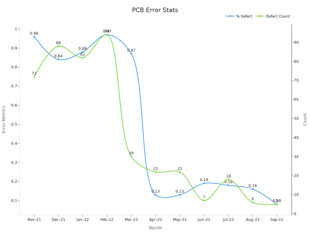
| Month | Boards Made | Defects Found | Defect Rate (%) |
|---|---|---|---|
| Nov–21 | 7512 | 72 | 0.96 |
| Dec–21 | 10,486 | 88 | 0.84 |
| Jan–22 | 9282 | 82 | 0.88 |
| Feb–22 | 9674 | 94 | 0.97 |
| Mar–22 | 3444 | 30 | 0.87 |
| Apr–22 | 17,284 | 22 | 0.13 |
| May–22 | 17,284 | 22 | 0.13 |
| Jun–22 | 3612 | 7 | 0.19 |
| Jul–22 | 10,072 | 18 | 0.18 |
| Aug–22 | 3696 | 6 | 0.16 |
| Sep–22 | 6156 | 5 | 0.08 |
The chart below shows how defect rates dropped over time. This proves that fixing errors improves quality:
How to Fix Errors
- Wrong Footprints: Check part sizes with datasheets to avoid mistakes.
- Trace Width Problems: Use tools to find the right width for your design.
- Unconnected Pins: Test the board to find and fix missing links.
- Overlapping Paths: Use DRC tools to spot and fix overlapping paths.
Callout: A study showed better pad spacing lowered defect rates from 0.96% to 0.08%. Careful design makes a big difference.
Fixing these common mistakes improves your PCB‘s quality and reliability.
File Generation and Documentation
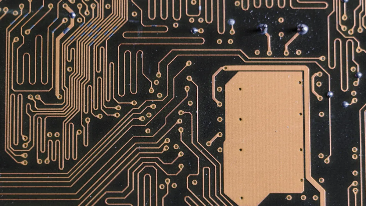
Gerber Files and Drill Files Creation
Gerber files are like maps for making PCBs. They show details about layers, like copper paths and solder masks. These files help manufacturers build your board correctly.
To make Gerber files, finish your PCB design and check it. Then, create files for each layer, like the top copper and solder mask. Design software makes this easy with built-in tools. You also need a drill file to guide hole-making.
Gerber files are very important for production. They help with UV light processes to form the PCB. They also ensure holes are drilled right and add labels like part names. Setting up the file generator properly avoids mistakes and speeds up production.
Bill of Materials (BOM) Preparation
A BOM lists all the parts needed for your PCB. It includes details like how many parts you need and their costs. This helps avoid running out of parts during production.
Using a BOM has many benefits. It helps plan costs and prevents surprises with prices or missing parts. Updating the BOM often keeps everything organized. It also helps manage inventory, so you don’t buy too much or too little.
A good BOM makes teamwork easier. It gives clear steps for putting the board together. This reduces mistakes and improves quality. Planning materials ahead saves money and keeps the product high-quality.
Assembly Drawings and Documentation
Assembly drawings show how to put the PCB together. They include diagrams that show where each part goes and how it fits. These drawings can be 2D, 3D, or exploded views for better understanding.
Clear assembly documents make production faster and easier. They remove confusion and help teams follow the design. For example, side views in the drawings show part positions clearly. Adding the BOM to the documents makes assembly smoother.
Industries like car and airplane makers have seen fewer mistakes and faster projects using detailed drawings. 3D PDFs also cut costs. Good documentation improves teamwork and ensures the PCB is made correctly.
Passing the Design to Manufacturing
Picking a PCB Maker
Choosing the right PCB maker is very important. Look for makers with the right skills and certifications for your project. For example, medical PCBs need ISO 13485 certification for safety. Car PCBs require IATF 16949 certification for quality and strength. The table below shows key certifications for different industries:
| Application Type | Needed Certifications and Standards |
|---|---|
| Medical Device PCBs | ISO 13485, strict quality checks, biocompatibility, cleanroom production |
| Automotive | IATF 16949, heat testing, vibration resistance, car-grade materials |
| High-Reliability | AS9100, NADCAP, strong testing, material tracking, secure facilities |
Also, check if the maker can handle your design’s complexity. Look at their production size and if they deliver on time. A good maker will give helpful feedback and support during production.
Sharing Design Details
Clear instructions help the PCB maker build your board correctly. Write simple and clear descriptions for each requirement. Use pictures or charts to explain tricky parts. For instance, a labeled diagram of the PCB layers helps the maker understand your design.
Use the same terms and format throughout to avoid confusion. Ask team members, like engineers, to review the details and suggest changes. Update the document when needed and track changes with version control. These steps reduce mistakes and keep everyone on the same page.
Checking Manufacturer Feedback
After sending your design, the maker will review it and share feedback. Pay attention to their advice, especially about making the design easier to produce. This includes adjusting your design to match their tools, picking the right materials, and using compatible file types.
Work closely with the maker to fix any issues quickly. Make changes to improve how easy it is to produce your PCB. This step lowers costs and speeds up production. Good communication ensures your design moves smoothly to manufacturing.
The PCB design process turns ideas into working circuit boards. Every step, like making schematics, layouts, and checks, is important. These steps ensure the board works well and can be built easily. Checking for mistakes early and keeping clear records helps avoid problems. Following good practices, like using design rules and trusted tools, makes better boards. Staying careful and organized helps create designs that last and meet industry needs.
FAQ
What does a PCB stackup do?
A PCB stackup arranges the layers of your circuit board. It helps signals stay clear, reduces EMI (electromagnetic interference), and spreads heat evenly. A good stackup also makes building the board easier and keeps it strong.
Tip: Ask your manufacturer for stackup advice to match their tools.
How do you pick the best PCB design software?
Choose software based on your project and skill level. Beginners may like easy tools like KiCad. Experts often use Altium Designer for features like 3D views and signal checks.
Note: Make sure the software supports needed file types like Gerber files.
Why is the Design Rule Check (DRC) useful?
The DRC checks if your PCB design follows safety and building rules. It finds problems like wrong trace sizes, spacing errors, or overlapping parts. Fixing these early avoids delays and makes a better board.
What are Gerber files, and why do they matter?
Gerber files are used to make PCBs. They show details about each layer, like copper paths and solder masks. Makers use these files to build your board exactly as designed.
How can you stop signal interference in PCB design?
You can reduce signal problems by keeping traces apart, adding ground planes, and routing fast signals carefully. Using differential pair routing (matching two paths) also keeps signals steady in high-speed designs.
Emoji Tip: 🛠️ Test for interference with simulation tools before finishing your design.