Difficulties in manufacturing and assembling industrial automation control PCBs
Industrial automation control PCBs serve as the backbone of modern manufacturing systems, enabling precise control and seamless integration of machinery. Their importance continues to rise due to the rapid growth of automation-dependent industries.
- The global industrial automation market, valued at $177.57 billion in 2021, is projected to reach $441.7 billion by 2030, with an annual growth rate of 8.84%.
- The robotics market is set to expand from $59.7 billion in 2022 to over $200 billion by 2030, reflecting a CAGR of 16.1%.
However, developing these advanced PCBs comes with significant challenges. Manufacturers face obstacles such as material shortages, complex designs, and stringent quality control demands. Overcoming these manufacturing difficulties is essential to meet the growing demand for reliable and high-performance PCBs in industrial automation.
Manufacturing Difficulties in Industrial Automation Control PCBs
Material Shortages and Supply Constraints
Material shortages and global supply chain disruptions have become a significant challenge for PCB manufacturing. The reliance on critical raw materials like palladium, titanium, and gallium, sourced from politically unstable regions, exacerbates the problem. For instance, Russia supplies 30% of the world’s palladium, while the United States imports 90% of its titanium and 100% of its gallium. These dependencies increase the risk of supply interruptions, leading to longer lead times and rising material costs.
The semiconductor chip shortfall further compounds the issue, affecting timely delivery of high-quality products. Port congestion and commodity price hikes add to the complexity, making components sourcing difficulties a persistent concern. Manufacturers must navigate these disruptions while maintaining production schedules and ensuring demand forecasting accuracy.
Complex Designs and High-Density Layouts
The evolution of integrated circuit packaging technology has led to increasingly complex PCB designs. High-density layouts now feature tripled leads per square inch and quadrupled components compared to 15 years ago. Additionally, the number of pins in a design has tripled, while pin-to-pin connections have doubled. These advancements, while necessary for modern industrial automation systems, pose significant manufacturing challenges.
| Metric | Value |
|---|---|
| Leads per square inch increase | Tripled in the last 10 years |
| Average number of components | Quadrupled in 15 years |
| Average leads-per-part decrease | 4 to 5 times |
| Number of pins in a design | Tripled |
| Number of pin-to-pin connections | Doubled |
| Percentage of companies citing complexity as a challenge | 53% |
Traditional defect detection methods struggle to meet the precision requirements of these intricate designs. High-volume production demands automated and intelligent technologies to ensure quality control and traceability. Without these advancements, manufacturers risk compromising the reliability of their products.
Quality Control and Traceability in Production
Maintaining quality control and traceability is essential in PCB manufacturing, especially for high-volume production. Differentiating responsibilities between Quality Assurance (QA) and Quality Inspection (QI) ensures that QA establishes quality measures while QI executes inspections. Statistical analysis of yield rates, defect rates, and customer return rates helps identify trends and implement corrective actions.
Traceability systems play a crucial role in tracking raw materials, process parameters, and inspection results. These systems enable manufacturers to quickly identify and address quality issues, ensuring consistent production of high-quality products. Non-conforming product control procedures further enhance quality management by segregating and reviewing defective items.
Despite these measures, challenges persist. Manufacturing defects, such as poor soldering or misplacement of parts, often go undetected due to inadequate testing processes. In safety-critical industries, the cost of addressing these defects can be substantial. Factories operating at low productivity levels face higher manufacturing costs, emphasizing the need for efficient quality control systems.
Cost Management in Manufacturing Processes
Effective cost management plays a pivotal role in the manufacturing of industrial automation control PCBs. Manufacturers must balance quality, efficiency, and affordability to remain competitive in a market that demands precision and reliability. Poor cost management can lead to financial losses, production delays, and compromised product quality.
Challenges in Cost Management
Cost management in PCB manufacturing often involves navigating a complex web of decisions. Selecting the cheapest fabricator may seem cost-effective initially, but it frequently results in higher overall expenses. Failed prototypes incur costs beyond the board itself, including wasted components, labor, and extended timelines. These setbacks can disrupt production schedules and erode customer trust.
📉 Tip: Investing in high-quality fabricators upfront reduces the risk of costly respins and ensures consistent performance.
Manufacturers also face challenges in low-volume PCB assembly, where economies of scale are harder to achieve. Smaller production runs often lead to higher per-unit costs due to fixed overheads and setup expenses. Additionally, sourcing premium materials for low-volume PCB assembly can strain budgets, especially when global supply chain disruptions inflate prices.
Strategies for Cost Optimization
To mitigate these challenges, manufacturers employ several strategies:
- Prioritizing Quality Over Short-Term Savings: Choosing reliable fabricators and suppliers minimizes the risk of defects and failures.
- Streamlining Processes: Automation and lean manufacturing techniques reduce waste and improve efficiency.
- Investing in Advanced Technologies: High-precision equipment ensures accuracy in low-volume PCB assembly, reducing the likelihood of errors.
- Collaborating with Trusted Partners: Long-term partnerships with suppliers foster stability and better pricing agreements.
The ROI of Smart Cost Management
Smart cost management decisions yield significant returns on investment (ROI). By prioritizing quality and efficiency, manufacturers avoid the financial burden of repeated respins and failed prototypes. This approach not only saves money but also enhances customer satisfaction and brand reputation.
| Decision Type | Potential Outcome |
|---|---|
| Choosing cheapest fabricator | Higher costs due to failures and respins |
| Investing in quality upfront | Reduced risk, consistent performance |
| Poor material sourcing | Increased costs due to delays and inefficiencies |
Manufacturers who adopt proactive cost management strategies position themselves for long-term success in the competitive PCB industry.
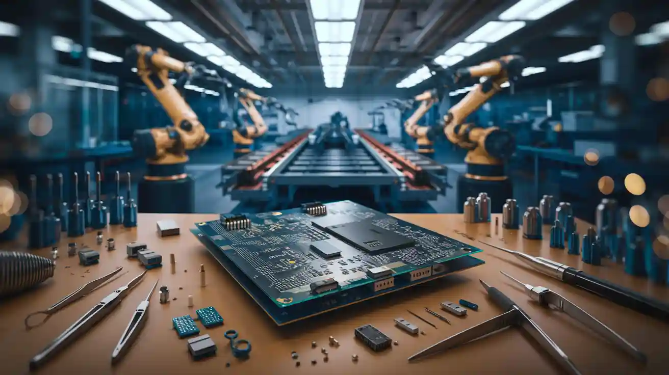
Assembly Challenges in PCB Production
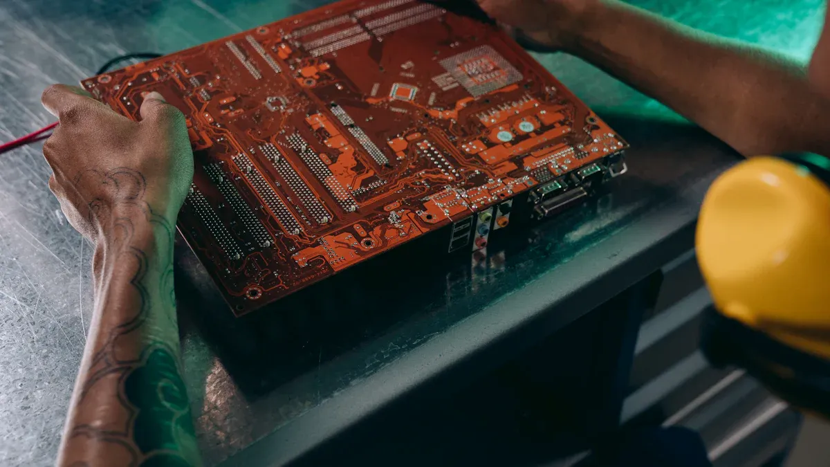
Precision in Component Placement
Precision in component placement is a cornerstone of successful PCB assembly. Industrial automation control PCBs demand exact positioning of components to ensure optimal functionality and reliability. Even minor inaccuracies can lead to electrical short circuits, impaired connectivity, or complete board failure.
Modern PCB assembly processes rely heavily on automated pick-and-place machines to achieve high precision. These machines use advanced algorithms and vision systems to position components accurately. However, challenges persist due to the increasing miniaturization of components and the complexity of high-density layouts. Manual assembly, often employed for low-volume production, introduces variability in quality due to human error.
| Metric | Description |
|---|---|
| Defects per Million Opportunities (DPMO) | Measures the number of defects found per million opportunities for defects, allowing for standardized comparisons. |
| First Pass Yield (FPY) | Represents the percentage of PCBs passing all inspections on the first attempt, indicating process efficiency. |
| Rework Rate | Measures the percentage of PCBs requiring additional work after initial assembly, with a low rate indicating high quality. |
| Scrap Rate | Represents the percentage of unusable PCBs due to defects, with a lower rate indicating better productivity. |
To address these challenges, manufacturers invest in high-precision equipment and advanced software solutions. Automated assembly systems reduce variability and improve consistency, ensuring better quality and higher yield rates.
Soldering and Thermal Management Issues
Soldering plays a critical role in PCB assembly, connecting components to the board and ensuring electrical conductivity. However, soldering challenges often arise due to material quality, process consistency, and environmental conditions.
- Material Quality: High-quality components and PCBs are essential for reducing defects.
- Process Consistency: Consistent soldering processes and accurate component placement are critical to avoid solder defects.
- Environmental Conditions: Cleanliness and controlled temperature and humidity levels are necessary to maintain assembly quality.
Thermal management is equally important, especially for high-density boards. Excessive heat during soldering can damage components, while insufficient heat may result in weak solder joints. Lead-free soldering compounds, which require higher melting points, further complicate the process.
Manufacturers mitigate these issues by implementing strict process controls and using advanced soldering techniques like reflow soldering. Automated systems ensure uniform heat distribution and reduce the risk of thermal damage. Additionally, maintaining clean and controlled environments minimizes contamination and improves assembly quality.
Testing High-Density and Multi-Layer Boards
Testing high-density and multi-layer PCBs presents unique challenges due to their intricate designs and compact layouts. Misaligned layers, voids in vias, and defects in buried or blind vias are common issues that require advanced testing methods to detect.
| Testing Method | Description |
|---|---|
| Optical Microscopy | Used for appearance inspection to identify failed parts and assess failure modes. |
| X-ray Inspection | Utilized for internal defect inspection, particularly in high-density packaged devices. |
| Automated X-ray Inspection (AXI) | Detects internal defects in multi-layer PCBs, such as misaligned layers and voids in vias. |
Testing complexity increases with the density of components and the number of layers. Traditional methods like optical microscopy may not suffice for identifying internal defects. Manufacturers often employ advanced techniques such as automated X-ray inspection (AXI) and flying probe testing to ensure comprehensive quality checks.
- PCB design complexity influences the choice of testing methods.
- High-density boards may require advanced techniques like flying probe or impedance testing.
Investing in robust testing protocols is essential for maintaining high-quality standards. These measures help manufacturers identify and rectify defects early, reducing rework rates and improving overall productivity.
Miniaturization and Handling Smaller Components
Miniaturization has become a defining trend in the electronics industry, particularly in the production of industrial automation control PCBs. As devices shrink in size, manufacturers face mounting challenges in handling smaller components during the assembly process. These components, often measured in millimeters or micrometers, demand exceptional precision and advanced techniques to ensure proper placement and functionality.
Challenges in Miniaturization
Handling smaller components introduces several challenges that complicate the assembly process. First, the reduced size of components increases the likelihood of misalignment during placement. Even a slight deviation can compromise the electrical connectivity of the PCB, leading to performance issues or complete failure. Second, miniaturized components often require specialized tools and equipment for accurate assembly. Standard pick-and-place machines may struggle to handle these tiny parts, necessitating upgrades to more advanced systems.
Another challenge arises from the fragility of smaller components. These parts are more susceptible to damage during handling and soldering. Excessive force or improper thermal management can render them unusable, increasing the scrap rate and driving up production costs. Additionally, the compact nature of high-density PCBs leaves little room for error, making defect detection and rework more difficult.
Strategies for Managing Miniaturization
Manufacturers employ several strategies to address these challenges and improve assembly outcomes.
- Advanced Placement Technologies: High-precision pick-and-place machines equipped with vision systems ensure accurate positioning of components. These systems use algorithms to detect and correct placement errors in real time.
- Specialized Handling Tools: Tools designed for micro-scale components reduce the risk of damage during assembly. For example, vacuum-based handling systems minimize physical contact with fragile parts.
- Enhanced Soldering Techniques: Reflow soldering processes tailored for miniaturized components ensure consistent heat distribution, reducing the risk of thermal damage.
- Rigorous Quality Control: Automated inspection systems, such as optical and X-ray technologies, detect defects in small components and high-density layouts. These systems enable manufacturers to identify issues early and minimize rework rates.
The Role of Workforce Training
Miniaturization also underscores the importance of workforce training. Operators must develop specialized skills to handle smaller components effectively. Training programs focused on precision techniques and equipment operation enhance assembly quality and reduce variability. By investing in workforce development, manufacturers ensure their teams can adapt to the demands of miniaturized PCB production.
Benefits of Overcoming Miniaturization Challenges
Successfully managing miniaturization challenges yields significant benefits for manufacturers. Improved assembly processes lead to higher first-pass yield rates, reducing the need for costly rework. Enhanced precision and quality control minimize scrap rates, lowering production costs and increasing profitability. Additionally, the ability to produce reliable, compact PCBs strengthens customer trust and positions manufacturers as leaders in the industry.
Miniaturization continues to push the boundaries of PCB assembly, demanding innovation and adaptability from manufacturers. By leveraging advanced technologies, specialized tools, and workforce training, they can overcome these challenges and meet the growing demand for smaller, more efficient industrial automation control systems.
PCB Supply Chain Management and Compliance-King Field
Sustainability and Environmental Regulations
Sustainability has become a cornerstone of modern PCB supply chain management. Companies face increasing pressure to reduce their environmental impact while maintaining operational efficiency. This challenge is compounded by the complexity of adhering to diverse environmental regulations across regions. Regular audits help manufacturers ensure compliance with these regulations, safeguarding both their reputation and operational continuity.
The demand for greener electronics has also grown significantly. Manufacturers must adopt eco-friendly materials and processes to meet stakeholder expectations and reduce their carbon footprint. Partnering with suppliers who prioritize sustainability ensures access to compliant materials while fostering long-term collaboration. Standardized reporting in sustainability metrics further enhances transparency and accountability, enabling companies to track progress and address sustainability and compliance issues effectively.
| Key Challenges | Strategies to Overcome |
|---|---|
| Keeping up with changing environmental regulations across different regions. | Conduct regular audits to ensure compliance with environmental and safety regulations. |
| Meeting the demand for greener electronics and reducing the carbon footprint. | Partner with suppliers offering eco-friendly materials that comply with global standards. |
Meeting Industry Standards and Certifications
Adhering to industry standards and certifications is critical for ensuring the quality and reliability of PCBs. Standards such as ISO 9001 and IPC-A-610 set benchmarks for manufacturing excellence, guiding companies in maintaining consistent quality. Compliance with these standards not only enhances product reliability but also builds customer trust.
Verifying compliance across jurisdictions remains a significant challenge. Companies must navigate varying regulatory frameworks while ensuring their processes align with global standards. This requires robust internal systems and collaboration with certified suppliers. Stakeholder pressure further drives the need for transparency, compelling manufacturers to adopt rigorous quality assurance practices. By meeting these standards, companies position themselves as leaders in the competitive PCB market.
- The importance of standardized reporting in sustainability metrics is emphasized, which is crucial for compliance in PCB supply chains.
- Challenges in verifying compliance across different jurisdictions highlight the need for better regulatory frameworks.
- Stakeholder pressure is a significant driver for companies to ensure compliance and transparency in their supply chains.
Achieving a Win-Win Sustainable Partnership
Sustainable partnerships in PCB supply chain management offer mutual benefits for manufacturers and suppliers. Collaboration fosters trust, enabling both parties to align their goals and achieve long-term success. Open communication plays a pivotal role in resolving issues quickly and ensuring smooth operations.
Encouraging supplier development drives innovation, enhancing competitiveness and efficiency across the supply chain. Proactive risk management further minimizes disruptions, ensuring business continuity. These factors contribute to a win-win scenario, where both manufacturers and suppliers thrive in a sustainable ecosystem.
| Aspect of SRM | Description |
|---|---|
| Collaboration and Trust | Effective SRM fosters collaboration and trust between suppliers and buyers. |
| Communication | Open communication leads to better alignment of goals and faster issue resolution. |
| Innovation | Encouraging supplier development drives continuous improvement. |
| Risk Management | Proactive risk management minimizes disruptions and ensures continuity. |
By prioritizing sustainability and fostering strong partnerships, companies can navigate the complexities of PCB supply chain management while achieving operational excellence.
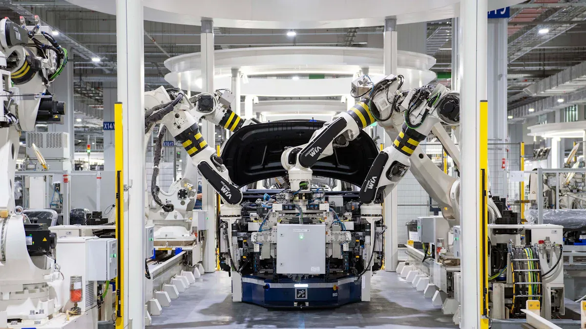
Solutions to Overcome Manufacturing and Assembly Challenges
Leveraging Advanced Manufacturing Technologies
Advanced manufacturing technologies (AMTs) have revolutionized the production of industrial automation control PCBs. By automating processes, manufacturers achieve higher precision, reduced error rates, and improved efficiency. For instance, automated assembly systems have significantly enhanced production capacity and quality.
| Metric | Before Automation | After Automation | Improvement |
|---|---|---|---|
| Production Capacity | 10,000 units/day | 85,000 units/day | Increased by 750% |
| Defect Rate | 2% | 0.02% | Decreased by 99% |
| First-pass Yield | 92% | 99.7% | Improved by 8.7% |
These technologies also optimize resource utilization. For example, energy consumption per unit decreases by 42%, while labor costs drop by 78%. Beyond operational benefits, AMTs enhance competitiveness by improving product quality and reducing time-to-market. Companies adopting these technologies report increased market share and agility, positioning themselves as leaders in the PCB industry.
Strengthening Clients Relationships
Strong client relationships are essential for overcoming challenges in PCB manufacturing and assembly. Open communication fosters trust and ensures alignment with customer expectations. Regular updates on production progress and proactive issue resolution build confidence and loyalty.
Manufacturers can further strengthen relationships by offering tailored solutions. For example, collaborating with clients to design custom PCBs that meet specific requirements enhances satisfaction. Additionally, annual customer visits provide opportunities to align production strategies with client development plans, ensuring long-term partnerships.
Investing in customer education also adds value. By providing insights into the manufacturing process, companies empower clients to make informed decisions. This collaborative approach not only improves customer retention but also enhances the overall reputation of the manufacturer.
Implementing Comprehensive Testing Protocols
Comprehensive testing protocols are critical for ensuring the reliability and safety of PCBs. Modern PCBs, with their complex designs and high-density layouts, demand rigorous testing to identify defects such as soldering issues and component misplacements. Effective testing mitigates risks and reduces costs associated with poor quality, which can account for over 40% of annual sales in the PCB industry.
- Testing uncovers common defects like soldering errors and lifting issues.
- Companies operating at Three Sigma quality levels spend 25% of revenue on remediating poor quality costs.
- Regular testing enhances brand reputation by maintaining a track record of high-quality products.
Advanced testing methods, such as automated X-ray inspection and flying probe testing, ensure thorough quality checks. These techniques detect internal defects in multi-layer boards, improving first-pass yield rates and reducing rework. By implementing robust testing protocols, manufacturers deliver reliable products while minimizing production delays and warranty claims.
Investing in Workforce Training and Development
Workforce training and development are essential for improving efficiency and productivity in PCB manufacturing. Many manufacturers struggle with onboarding processes and effective training systems, which can hinder operational performance. Investing in workforce development ensures employees acquire the skills needed to adapt to technological advancements and meet industry demands.
Organizations that prioritize training often see measurable improvements in workforce efficiency. For example:
- Enhanced onboarding processes reduce the time required for new employees to become productive.
- Retention strategies improve employee satisfaction, minimizing turnover rates.
- Training programs focused on change management help teams adapt to disruptive technologies.
Nittany Paper Mills provides a compelling example of the impact of workforce training. When introducing new equipment, they recognized the need for skilled management to lead change effectively. By investing in training for their managers, they maximized the benefits of their technological investments. This approach highlights the importance of equipping employees with the knowledge and tools to handle innovations in PCB assembly processes.
Manufacturers can implement training programs tailored to specific roles, such as assembly technicians or quality control specialists. These programs should emphasize precision techniques, equipment operation, and troubleshooting skills. Regular assessments ensure employees retain knowledge and apply it effectively in their roles. By fostering a culture of continuous learning, companies enhance productivity and maintain a competitive edge in the PCB industry.
Implement Annual Customer Visits-Connect with company development plan
Annual customer visits play a vital role in strengthening relationships and aligning production strategies with client development plans. These visits provide manufacturers with valuable insights into customer needs, enabling them to tailor their PCB assembly processes accordingly. They also foster trust and collaboration, which are critical for long-term partnerships.
During these visits, manufacturers can showcase their capabilities and discuss upcoming innovations. This proactive approach helps clients understand how new technologies and processes can benefit their operations. For instance, manufacturers might demonstrate advancements in assembly techniques that improve precision and reduce defect rates. These discussions create opportunities for joint planning and innovation.
Customer visits also serve as a platform for gathering feedback. Manufacturers can identify areas for improvement and address concerns directly. This feedback loop enhances product quality and ensures alignment with customer expectations. Additionally, visits provide an opportunity to discuss future goals and explore ways to integrate them into the company’s development plan.
By prioritizing annual customer visits, manufacturers build stronger relationships and foster collaboration. These interactions not only improve customer satisfaction but also position the company as a trusted partner in the PCB industry.
Industrial automation control PCBs face numerous challenges, including material shortages, complex designs, and precision assembly requirements. These obstacles demand innovative solutions to ensure high-quality production. Proactive strategies, such as leveraging AI and machine learning for automation, digital twin technology for accurate simulations, and augmented reality for streamlined documentation, have proven essential. Collaboration tools further enhance communication, optimizing processes across teams.
| Key Point | Description |
|---|---|
| AI and Machine Learning | Automates processes in PCB production, enhancing efficiency. |
| Digital Twin Technology | Provides accurate simulations for better design and production outcomes. |
| Enhanced Collaboration Tools | Improves communication between teams, crucial for optimization. |
| Augmented Reality | Aids in assembly documentation, streamlining the production process. |
Prioritizing quality, efficiency, and adaptability yields measurable benefits. Faults decrease, lead times shorten, and production costs drop significantly. For example:
- Lot reject rates improved from 5500 PPM to 900 PPM.
- Defect rates fell from 3.5% to less than 0.5%.
- Production capacity increased by 300%, while time-to-market accelerated by 40%.
By embracing innovation and fostering collaboration, manufacturers can overcome challenges and maintain a competitive edge in the evolving PCB industry.
FAQ
What are the most common defects in PCB manufacturing?
The most frequent defects include soldering issues, misaligned components, and thermal damage. These problems often arise from process inconsistencies or inadequate quality control. Manufacturers mitigate these risks by employing advanced inspection systems and adhering to strict production protocols.
How does miniaturization impact PCB assembly?
Miniaturization increases the complexity of component placement and soldering. Smaller components demand higher precision and specialized tools. Manufacturers address these challenges by investing in advanced pick-and-place machines and reflow soldering techniques, ensuring accurate assembly and reducing defect rates.
Why is traceability important in PCB production?
Traceability ensures that manufacturers can track materials, processes, and inspection results throughout production. This capability helps identify and resolve quality issues quickly, ensuring consistent product reliability. It also supports compliance with industry standards and enhances customer trust.
What role does workforce training play in PCB manufacturing?
Workforce training equips employees with the skills needed to operate advanced equipment and adapt to technological changes. Effective training programs improve productivity, reduce errors, and enhance overall product quality. Companies that prioritize training maintain a competitive edge in the industry.
How do manufacturers manage supply chain disruptions?
Manufacturers address supply chain disruptions by diversifying suppliers, maintaining safety stock, and leveraging demand forecasting tools. Collaboration with trusted partners and adopting flexible procurement strategies also help mitigate risks and ensure uninterrupted production.