How to Ensure Reliable Performance in Rigid Flex PCB Design

You want your rigid flex pcb design to work well for a long time. It should also keep working when things get tough. How reliable it is depends on how you deal with electrical and mechanical things. If you do not fix some problems early, your design can fail.
- Keeping impedance the same in all layers is hard.
- Not using the right bend radius can cause cracks.
- You must plan trace routing for signals and heat.
- Putting parts near bends can hurt them when you bend the board.
- Talking to fabricators early helps you not make expensive mistakes.
You should always make sure your rigid flex pcb is strong and works well. Good design means you know about these problems and fix them first.
Key Takeaways
- Keep impedance the same on every layer. This helps signals stay strong and stops data errors.
- Use the right bend radius rules. This keeps your rigid flex PCB from cracking and makes it last longer.
- Talk with fabricators early in the design. This helps you avoid expensive mistakes and makes building easier.
- Use arched trace routing. This lowers stress and helps your PCB last longer, especially in flex parts.
- Pick good materials like polyimide for flex sections. These can handle tough conditions and keep your PCB working well.
Electrical Integrity in Rigid Flex PCB Design
You need to pay attention to electrical integrity in rigid flex pcb design. Good electrical performance makes your board last longer and work better. You should follow steps for impedance control, signal integrity, and stack-up symmetry.
Impedance Control
Impedance is very important in rigid flex pcb. If you do not control impedance, signals can bounce and cause trouble. This might make data wrong or even break the system. You want the impedance to stay the same on every layer, especially in fast designs.
- Controlled impedance lets signals move fast and clear.
- You need to balance trace width, dielectric material, and space between layers.
- Rigid flex pcb design often uses thicker cores, like 2 to 4 mils, to meet impedance needs.
- Sometimes, you need thinner traces or more space for higher impedance.
Tip: Impedance control is needed in things like smartphones and computers. It keeps signals strong and stops them from mixing up.
You can check impedance with special tools. Here are two ways to do it:
| Technique | Description |
|---|---|
| Time-Domain Reflectometry (TDR) | Sends signals and checks for reflections to test impedance. |
| Test Coupons | Small test pieces that copy the board’s impedance for easy checking. |
You should always test impedance before you finish your design. This helps you meet all impedance needs and stops surprises.
Signal Integrity
Signal integrity means your signals stay strong and clear as they move. You want to stop noise, crosstalk, and reflections. These problems can happen if you do not route well or use the wrong materials.
- Use controlled impedance routing to keep signals steady.
- Keep traces apart to lower crosstalk.
- Add shielding to block outside noise.
- Pick materials with a stable dielectric constant for better signals.
- Use differential pair routing and match trace lengths for fast signals.
- Give each signal a solid return path, like a ground plane.
Note: Good signal integrity keeps your board working, even in hard places. It also helps you meet all electrical needs.
You should plan power distribution too. Good power planes keep voltage steady and lower power loss. You must also think about heat. Good thermal management keeps your board cool and safe.
Stack-Up Symmetry
Stack-up symmetry is important for reliability in rigid flex pcb design. If your stack-up is not balanced, your board can bend or twist. This can change impedance and cause problems.
- Keep the same number of layers and thickness on both sides.
- In a 6-layer design, you can use a 2-layer flex part and a 4-layer rigid part, but keep the dielectric thickness even.
- Spread copper out evenly. Do not put too much on one side.
- Symmetry helps your board handle heat and stress without bending.
Alert: If your stack-up is not even, your board can warp, get stressed, and fail more. Always check your stack-up before building.
Stack-up optimization means you plan your layers to meet all impedance needs and keep your board flat. This step is important for both electrical and mechanical strength.
By following these steps, you can meet all needs for impedance, signal integrity, and stack-up symmetry. This will help you make a rigid flex pcb that works well and lasts a long time.
Mechanical Layout and Durability

Bend Radius Guidelines
You need to follow bend rules to keep your rigid flex pcb strong. If you bend the board too far, it might crack or break. The right bend radius depends on how many layers you have and how you use the board. If the board only bends sometimes, use a bigger radius for more layers. If the board bends a lot, the radius should be even larger. The table below shows the smallest bend radius you should use for each flex circuit type:
| Flex Circuit Type | Static Bend Radius | Dynamic Bend Radius |
|---|---|---|
| Single-layer | 6 × thickness (T) | 12 × thickness (T) |
| Double-layer | 12 × thickness (T) | 24 × thickness (T) |
| Multilayer (>2 layers) | 24 × thickness (T) | 48 × thickness (T) |
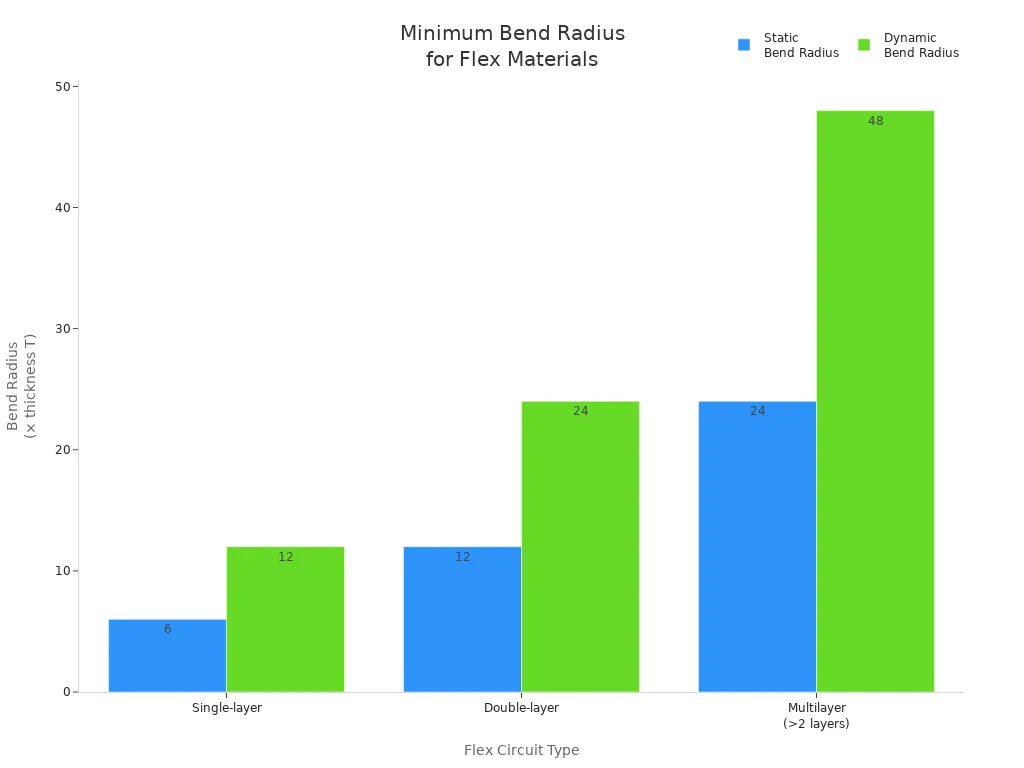
If you do not use the right bend radius, you can hurt the board and make it weaker. Always check the thickness and use the correct ratio for your board.
Smooth Transition Between Rigid and Flex Sections
You should make smooth changes between rigid and flex parts. Sharp changes can put stress on the board and cause cracks. Try these tips to help your board bend better:
- Make the change from rigid to flex slow and smooth.
- Line up copper layers with the middle of the bend.
- Draw traces with soft curves, not sharp corners.
- Do not put vias or parts close to the change area.
- Use thinner copper in flex parts to help them bend.
The table below shows what can go wrong if you do not follow these tips:
| Failure Mode | Description |
|---|---|
| Vias Near Rigid-Flex Transitions | Can cause stress and via failures. |
| Sharp Trace Angles | Lead to circuit fractures over time. |
| Stiffener-Related Failures | May cause cracking or delamination. |
| Imbalanced Stack-ups | Can warp the board and stress solder joints. |
Material Selection for Harsh Environments
You need to pick the right materials for tough places. Polyimide is good for flex parts because it can handle heat and chemicals. High-Tg FR-4 is strong for rigid parts. Rolled annealed copper bends well, and ENIG plating stops rust. For glue, use epoxy for strength or acrylic for shaking. Polyimide coverlays and coatings like parylene give extra safety.
A real test showed that polyimide tape, epoxy, and special oil helped a rigid flex pcb last through wet, hot, and rough drops. The board kept working with no bad connections. Picking good materials and putting parts in the right place helps your board stay strong and work well.
Trace Routing and Component Placement in Rigid-Flex PCB
Arched Trace Routing
You can make your rigid flex pcb last longer by using arched trace routing. Curved traces help spread out the stress when the board bends. This makes cracks and broken circuits less likely. Always use smooth, rounded corners in the flex area. Sharp angles can cause damage. Route traces so they cross the bend line straight up and down. This helps stop stretching and squeezing. Move traces and vias so they do not line up. This keeps the board from having weak spots.
Here are some good ways to use arched trace routing:
| Recommended Practice | Description |
|---|---|
| Smooth, Curved Traces | Spread out strain and lower the chance of cracks. |
| Staggering Vias and Traces | Spread out stress and stop weak spots from forming. |
| Uniform Trace Widths | Keep impedance the same and stop stress from building up. |
| Proper Clearance | Give traces space near changes to lower stress. |
Tip: Use real curved traces for every corner in the flex area. This helps the board move and bend without problems.
Optimal Via and Pad Placement
You need to put vias and pads in the right places to stop problems. Do not put vias close to where the rigid and flex parts meet. Vias in these spots can break when the board bends. If you use via-in-pad, fill the vias and make them flat. This keeps solder from going into the via and makes joints strong. Use wider traces in flex areas and do not make sharp bends. Pads should be round and not too big. This shape helps lower stress and keeps connections safe. Always make smooth changes between pads and traces.
Some problems from bad via and pad placement are:
| Issue | Explanation |
|---|---|
| Inadequate drill-to-copper spacing | Can cause shorts and make the board cost more to build. |
| Unoptimized transition zones | Glue can squeeze out and make the board weaker. |
| Abrupt changes in trace width | Make weak spots and can cause breaks. |
Avoiding Stress Points
You need to keep stress points away to make your rigid flex pcb strong. Curved traces help lower stress in one spot. Spread out stress in places that bend. Do not put vias or parts near places with lots of stress. Make slow, smooth changes between rigid and flex parts. Add extra layers or meander shapes in high-stress spots to help.
Stress points can make the board peel, swell, or crack. These problems can make the board fail early. You can use special shapes at pad-trace joins and put stiffeners in the right places to spread out stress. Tests like heating and bending the board help you find weak spots before making lots of boards. Good design and careful routing help you meet needs and make your board work better.
Collaboration with Fabricators
Early Design Reviews
You should begin your rigid-flex pcb project with early design reviews. These reviews help you find problems before building anything. Using the Design for Manufacturability process means you check your design with real factory limits. This step helps you see issues like wrong layer stackups or hard drill patterns. Fixing these problems early saves material and lowers costs. You also get better first-pass yield rates. Following standards like IPC-2221 during reviews helps you meet industry rules and avoid last-minute changes. Early reviews make your flexible circuit board easier to build and help it work better.
Tip: Early reviews help you save time and money by finding mistakes before making the board.
Communicating Requirements
Clear communication with your fabricator is important for a good flexible circuit board. You need to share all your requirements clearly. Good communication helps everyone know what the design should do and stops expensive mistakes. Here are some best ways to do this:
- Make graphics from MCAD tools to check if things fit.
- Give your fabricator a 3D animation to show how the board folds.
- Write down all sizes, stackup drawings, drill tables, impedance tables, and part outlines.
- Add clear notes that explain any special needs.
- Make sure your design and factory teams talk often.
If you follow these steps, you avoid confusion and make sure your needs are met. You also help your fabricator build the board the way you want.
Leveraging Fabricator Expertise
You can make your board easier to build and stronger by working with your fabricator. Their experience helps you pick the right materials and use the best design steps. They also help keep the quality high. The table below shows how fabricator skills help your project:
| Aspect | Impact on Reliability and Manufacturability |
|---|---|
| Material Selection | Boards handle stress and tough environments |
| Optimized Design Practices | Fewer failure points and better performance |
| Production Controls | High quality and consistent results |
Many fabricators offer advanced building, fast prototypes, and full DFM help. When you share what you know, you get better results. For example, a German solar company worked with a fabricator to make 200,000 multi-layer boards. Both teams learned from each other and made the product better. You can reach better performance by using your fabricator’s skills and keeping your needs clear.
You can make rigid flex PCB work better by using smart steps. First, decide how big and what shape your board will be. Plan how the layers will go together. Pick materials like polyimide for the board. Do not use sharp corners. Put stiffeners where the board needs more strength. Work with your fabricator and follow rules like IPC-2223 and IPC-6013D. Test your board by bending it and heating it up. Here is a checklist to help you:
- Pick materials that are strong.
- Keep impedance steady.
- Stay away from stress spots.
- Write down all details.
- Test your board before making many.
Doing these things helps your board last longer and work well.
FAQ
What is the most common cause of failure in rigid flex PCBs?
You often see failures from poor bend radius or sharp transitions. These mistakes create cracks or broken traces. Always follow bend guidelines and use smooth curves to keep your board strong.
How do you test the durability of a rigid flex PCB?
You can bend and heat your board many times. This process checks for cracks, delamination, or broken connections. Ask your fabricator about standard tests like flex cycling and thermal shock.
Which materials work best for flex sections?
Polyimide works best for flex areas. It handles heat and chemicals well. Rolled annealed copper also bends without cracking. You should avoid standard FR-4 in flex zones.
Can you place components on the flex part of the PCB?
You should avoid placing parts on flex sections. Bending can damage solder joints and parts. Place components on rigid areas for better reliability.