How to Create PCB Layouts That Simplify Assembly
Efficient printed circuit board (PCB) assembly design begins with smart layout choices. You help make good PCB designs by thinking about assembly early. Planning ahead gives you better yield rates and saves money. It also makes production faster and easier. Good planning changes results in these ways:
| Metric | Value |
|---|---|
| Yield Rates | Up to 95% |
| On-time Delivery Rates | 98% |
| Production Efficiency | Improved by 30% |
| Cost Reduction | Up to 20% |
You can make designs simpler by picking standard parts. Place parts in a logical way. Use simple design structures. These steps help you build strong PCB assembly designs. They make assembly quicker and easier.
Key Takeaways
- Start planning your PCB layout early to stop mistakes and make production faster. Planning early helps you get more good boards and saves money.
- Pick standard components to make assembly easier. Standard parts are simple to find, cost less, and help stop mistakes during making.
- Put components in a smart way to make assembly faster. Group the same parts together and make clear paths to stop problems and help the board work better.
- Keep enough space between parts to stop soldering problems. Enough space keeps parts from touching by accident and makes fixing things easier.
- Use clear silkscreen labels for better assembly. Good labels help machines and people put parts in the right place and stop mistakes.
PCB Assembly Design Principles
Early Planning for Assembly
When you plan for assembly early, you help your pcb assembly design work better. Planning ahead stops problems that can slow down making the boards or cause mistakes. If you think about assembly while designing, you make smarter choices for your printed circuit boards. Early planning helps fix many problems:
| Challenge | Solution |
|---|---|
| Supply Chain Issues | Partner with a reliable ECM partner for vetted suppliers and accurate part forecasting. |
| Irregular Board Sizes | Hire an ECM partner with an on-site engineering team to optimize design for standard components. |
| Inaccurate Solder Paste | Utilize expert inspections to detect defects before component placement to avoid rework. |
| Manufacturing Defects | Choose an ECM partner that employs automated optical inspection (AOI) throughout the assembly process. |
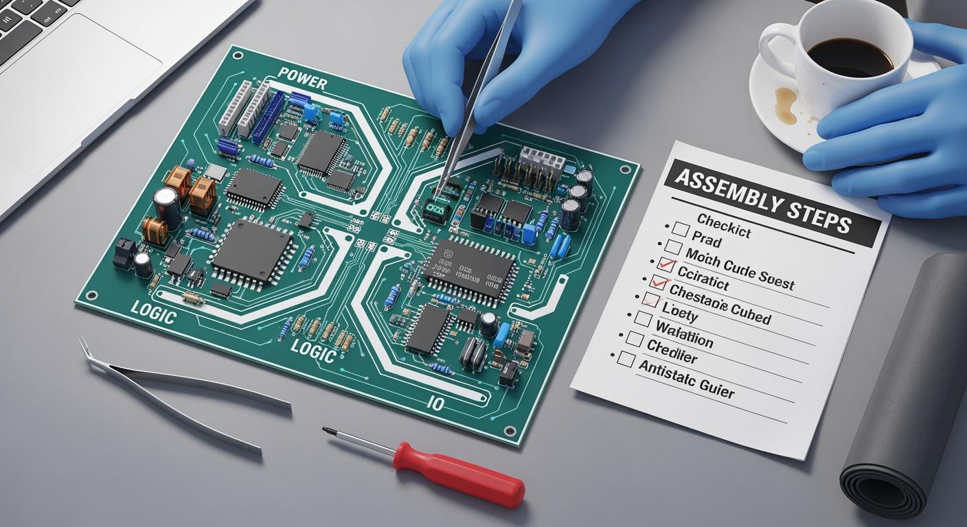
Tip: Make a checklist before you start your pcb assembly design. This helps you remember important steps and not miss anything that could cause mistakes.
Planning for assembly early helps you work faster and make fewer mistakes. It also helps you finish on time and spend less money.
Standardized Component Selection
Choosing standardized components makes pcb assembly design easier. Standard parts are simple to find and fit most pcb layouts. This choice helps you avoid delays and supply chain problems. You also save money because standard parts usually cost less and are easy to buy.
Picking standardized components means you get fewer quality problems and mistakes. You will see fewer installation issues, so you have less assembly errors and lower costs. When you use prefabricated parts, you do not need to change much during assembly. This saves time and keeps your boards safe during shipping. You also save money by making smart choices when you design.
- Using standardized components makes buying parts easier.
- It makes manufacturing less complicated.
- It helps you finish making boards faster.
Note: Always ask your supplier if your parts are available and not being discontinued.
Logical Component Placement
Logical component placement makes pcb assembly design better. Good placement means you put similar parts together in straight lines or grids. This helps machines pick and place parts quickly and correctly. Logical placement also stops mistakes that can cause defects or even pcb failure.
- Putting parts in the right place is very important in SMT assembly, because mistakes can cause defects, poor performance, or even pcb failure.
- Placement mistakes cause up to 60% of SMT assembly problems, so being careful is very important.
- If parts are not lined up right, signals can get messed up, especially in high-frequency boards, and this can hurt how well your product works.
You can follow these steps to make your design better for assembly:
- Use design for manufacturability rules to leave enough space between parts.
- Group and line up similar parts to help machines work faster and make fewer mistakes.
- Set up feeders and packaging the right way to stop pick-up errors.
Tip: Placing parts in smart spots makes assembly faster and helps your pcb designs work better.
Always check your layout for clear paths and do not put parts too close together. This makes soldering easier and stops problems like cold joints or tombstoning. Logical placement helps you make pcb layouts that are simple to build and test.
Optimize PCB Design for Spacing and Layout
Part-to-Part Spacing
You get better assembly when you leave enough space between parts on your pcb. Good spacing stops solder from connecting where it should not. It also makes fixing or soldering by hand easier. If IC sockets are too close to sensitive parts, solder joints can get stressed when you handle the board. Do not put sensitive parts in the middle of the pcb. This helps stop damage from bending or twisting. If you put BGA and lead-less packages on one side, it is easier to check and fix them. If you do not leave enough space, you might put parts in the wrong place, fail checks, and pay more to make the board. Crowded parts slow down assembly and make workers spend more time. To stop this, always look at your layout and keep space between parts.
- Leave space so solder does not connect parts by mistake.
- Do not put IC sockets next to sensitive parts.
- Keep sensitive parts away from the middle.
- Put BGA and lead-less packages on one side.
Grid and Trace Management
Making traces and spaces better is important for a strong pcb. You need to line up parts so soldering is even. Good footprints help with wave soldering and make sure parts face the right way. If parts are not lined up, solder can bridge and cause problems. Different packages can make stress inside the board, and solder joints must handle heat changes. Using good solder paste and keeping water out of pcbs helps soldering work well. Doing these things helps you get more good boards and fewer mistakes.
- Line up parts for even soldering.
- Make footprints so parts face the right way.
- Use good solder paste and keep water out.
Minimize Component Density
You make the pcb the right size and easy to build by not putting too many parts close together. Enough space stops mistakes and short circuits. A neat layout makes it easier to build and check the board. You should put parts that work together in groups and line them up for good signal flow. Using small packages and SMDs saves space. Adding thermal vias and more copper near hot parts helps with heat. To stop crowding, use CAD tools to find problems and ask others to check your work.
| Strategy | Description |
|---|---|
| Prioritize Readability And Spacing | Spread out parts and wires so things are not crowded or confusing. |
| Implement A Peer Review Process | Work with others to find mistakes early and stop layout problems. |
| Use CAD Systems Effectively | Use design rules to find and fix crowding problems automatically. |
You make your pcb design better by following these steps and keeping your layout neat and clear.
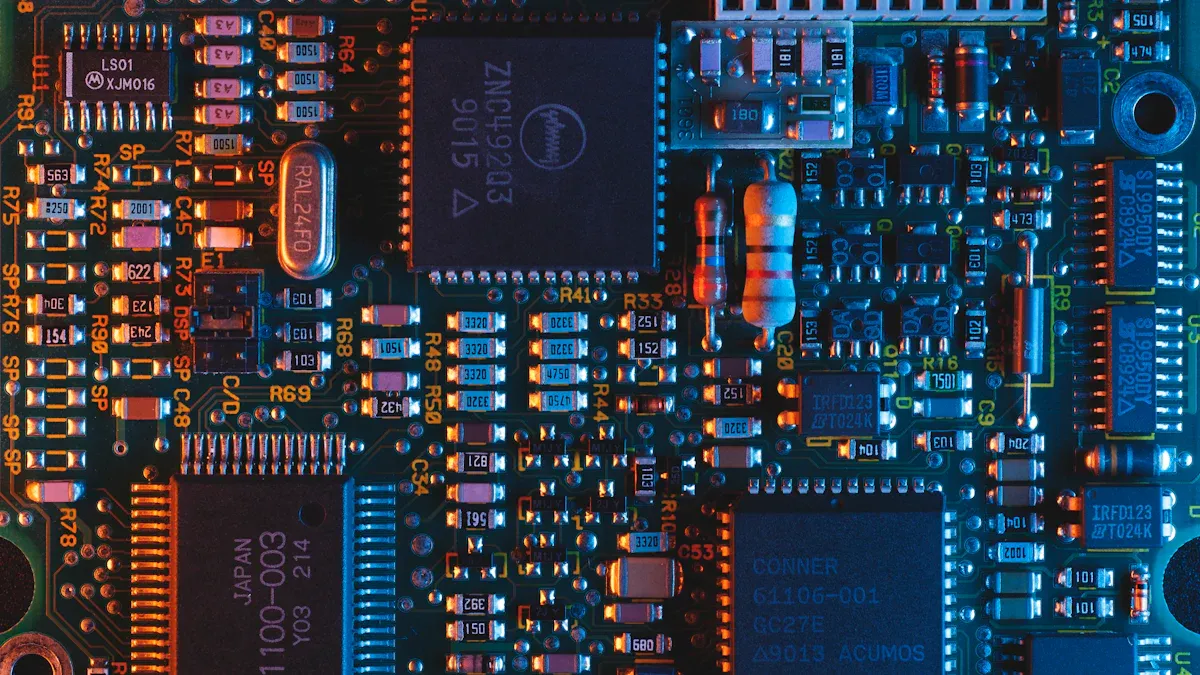
SMT Assembly Process Optimization
Single-Sided SMT Layouts
You can make smt assembly easier by putting all parts on one side. This lowers costs and makes building the board simple. You do not have to worry about parts getting mixed up or soldering mistakes. Many products made in large numbers use this way because it saves time and money.
| Advantage | Explanation |
|---|---|
| Cost-Effective | It costs less because only one side has parts. This is good for making lots of boards. |
| Simplicity and Ease of Manufacturing | The design is easy, so there are fewer mistakes and faster work. |
| Fewer Manufacturing Challenges | No parts on the back means fewer problems like parts not lining up or soldering errors. |
Tip: Try to put all SMT parts on one side. You will have fewer mistakes and finish faster.
Consistent Orientation
Machines work better when all SMT parts face the same way. Pick-and-place machines need parts lined up the same to work well. If you keep the same direction, you stop problems like tombstoning and parts not lining up. Even a small change in how you place parts can lower soldering mistakes by a lot. This is very important for good smt assembly.
- Keeping the same direction helps machines place parts right.
- Good placement stops mistakes like tombstoning.
- You get better boards with fewer problems.
Note: Always look at your layout before you start. Make sure all parts face the same way.
Proper Footprints and Pad Sizes
You need the right footprints to make strong solder joints. Pad sizes should follow what the maker says or use rules like IPC-7351. For example, a 0402 resistor or capacitor needs pads that are 0.5 mm by 0.6 mm with a 0.4 mm gap. An SOIC-8 package uses pads that are 0.6 mm wide and 1.5 mm long. Leave at least 0.1 mm between the pad edge and the solder mask opening. This stops solder from joining where it should not and keeps your board safe during smt assembly.
- Use the right footprint for each part.
- Make pad sizes match the rules.
- Leave enough space between pads and the solder mask.
Tip: Doing these things helps you make boards that last longer and work better.
DFM and Panelization for Efficiency
Follow Manufacturer DFM Guidelines
You get better assembly when you follow manufacturer dfm guidelines. These rules help you not make mistakes in design for fabrication and design for assembly. You will see more good boards and fewer problems if you use these standards. Manufacturers check your PCB layout for enough space, right pad sizes, and simple shapes. They look for things that could slow down making your boards or cause errors. DFM reviews find problems before you start making the boards, so you save time and money. You can spend up to 40% less if you use dfm guidelines and make your design better for fabrication. You also make design for assembly easier for people and machines.
- The design step matters most for getting good boards.
- Bad PCB designs can cause parts to be put in the wrong place and soldering problems.
- DFM checks find problems before you make the board.
- Following IPC standards gives you more good boards and fewer mistakes.
- Making the right number of layers and vias saves money.
Tip: Always ask your manufacturer for their design for fabrication checklist before you start your layout.
Add Fiducials and Tooling Holes
Your PCB is easier to build when you add fiducials and tooling holes. These things help machines line up your board for drilling, soldering, and putting on parts. Tooling holes keep every board in the same spot, which is important when you make a lot of boards. Machines use cameras to find these holes and put parts in the right place. Fiducial markers go in three corners of your PCB. They help machines know which way the board goes, so you get fewer mistakes and better results. Good alignment makes work faster and boards more alike.
- Tooling holes help put boards in the right spot fast.
- Keeping boards lined up helps every board in a group.
- Cameras use tooling holes to place parts right.
- Fiducials help stop mistakes and make assembly better.
PCB Panelization Techniques
You save time and money when you use smart panelization in design for fabrication and design for assembly. Panelization lets you put many PCBs on one big sheet, which means less waste and faster work. Mouse bites panelization uses tiny holes so you can break boards apart easily. This way works well for edge parts but may not be as exact. You can save 20-30% on costs for big jobs by using panelization. You also use up to 15% less material. Good panelization uses shapes and process knowledge to get more good boards and make assembly easier.
- Mouse bites panelization lets you break boards apart easily.
- Using materials and workers well means less waste.
- Many PCBs on one panel makes boards more alike and better.
- Panelization makes assembly faster and simpler.
Note: Plan your panelization early in your design for fabrication process to get the best results and spend less money.
Test Points and Labeling
Accessible Test Points
You make testing and troubleshooting much easier when you add accessible test points to your PCB. Good test point placement helps you check if your board works right after assembly. You should follow these best practices:
- Place test points near the edge of the board or in open areas away from tall parts. This makes it easy to reach them with probes.
- Cover all important nets, such as power lines and high-speed signals, with test points.
- Keep enough space between test points and sensitive traces. This protects signal quality.
- Do not group test points too close together. This prevents probe access problems and lowers the chance of crosstalk.
- Group related test points in open spots, but leave enough room for standard probes.
- Add special pads for power and ground. This makes it simple to connect and keeps signals steady.
- Leave clear space around each test pad. This stops accidental shorts and makes it easier to use test tools.
- Spread test points across the board. This helps you test the board better and makes test fixtures simpler.
- Use board connectors and headers as extra test access points when possible.
- Add jumpers or DIP switches to test parts by themselves.
- Design your board so you can enter test modes for easier debugging.
Tip: Well-placed test points save you time and help you find problems fast.
Clear Silkscreen Labels
Clear silkscreen labels help you avoid mistakes during assembly. High-resolution silkscreen makes markings easy to read. This is very important when your board has many parts close together. If a label is hard to read, you might put a part in the wrong place. This can cause your board to fail.
| Evidence Type | Description |
|---|---|
| Assembly Errors | High-contrast silkscreen colors help you make fewer mistakes, especially when placing parts by hand. |
| Automated Assembly | Machines use high-contrast colors to read markings. This lowers the risk of putting parts in the wrong spot by up to 15%. |
- Clear markings make even small text easy to read.
- Good labels help you find the right spot for each part.
- High-resolution printing lowers errors in both manual and machine assembly.
Note: Always check your silkscreen labels for clarity before sending your design to manufacturing. Clear labels help you build better boards with fewer errors.
You can make PCB assembly easier if you plan your layout. Pick standard parts and keep your design simple and clear. These steps help you build boards faster and make fewer mistakes. Using good practices makes your boards easier to build and stronger. It also helps signals move better on the board. Here is how these ideas help:
| Strategy | Outcome |
|---|---|
| Simplified design structures | Makes things less complicated and helps more boards work |
| Optimizing traces and spaces | Stops problems and makes boards work better |
| Early stage collaboration | Makes designs better for assembly |
Companies that use these steps have fewer mistakes and save money. You also get boards that are stronger and last longer. Try these ideas in your next project to get better results.
FAQ
What is the best way to choose components for easy PCB assembly?
You should select standard parts that are easy to find. Ask your supplier if the parts are available. Standard components help you avoid delays and make assembly faster.
How much space should you leave between PCB parts?
Leave enough space so solder does not connect parts by mistake. Most manufacturers suggest at least 0.5 mm between pads. Check your design rules for the best spacing.
Why do you need clear silkscreen labels on your PCB?
Clear silkscreen labels help you place parts in the right spot. You avoid mistakes during assembly. Machines and people read labels faster when they are easy to see.
What are fiducials and why do they matter?
Fiducials are small marks on your PCB. Machines use them to line up the board for assembly. Good fiducials help you get fewer errors and better results.