How to Optimize High-Speed PCB Design
High-speed PCB design has become a cornerstone of modern electronics, enabling the development of faster, smaller, and more efficient devices. The demand for miniaturization and advanced functionality has fueled the market, which is growing at a compound annual growth rate (CAGR) of over 7%. This trend reflects the rising adoption of IoT devices and other cutting-edge technologies. However, achieving reliable performance in high-speed designs requires addressing signal integrity, a critical factor that ensures accurate data transmission without distortion or loss.
Signal integrity issues, such as impedance mismatches, can lead to signal reflection and degradation, compromising the performance of high-speed circuits. Studies demonstrate that optimizing line impedance near discontinuities significantly enhances signal integrity, improving insertion loss up to 7 GHz and return loss by 5 dB. Designers must also contend with challenges like electromagnetic interference (EMI), crosstalk, and signal distortion, which demand careful planning and adherence to best practices.
Key Takeaways
- Focus on keeping signals clear for good data transfer in fast PCBs. Fix problems like signal mix-ups and interference to improve performance.
- Pick materials that lose less signal and work well at high speeds. This helps signals stay strong and reliable.
- Plan trace paths carefully by keeping them short and direct. This lowers signal problems and makes designs work better.
- Use simulation tools early to spot and fix design mistakes. These tools save time and make designs more accurate.
- Learn new tips from webinars and guides to stay skilled. Keeping up with trends helps designers stay ahead in PCB design.
Understanding High-Speed PCB Design
What qualifies as high-speed PCB design?
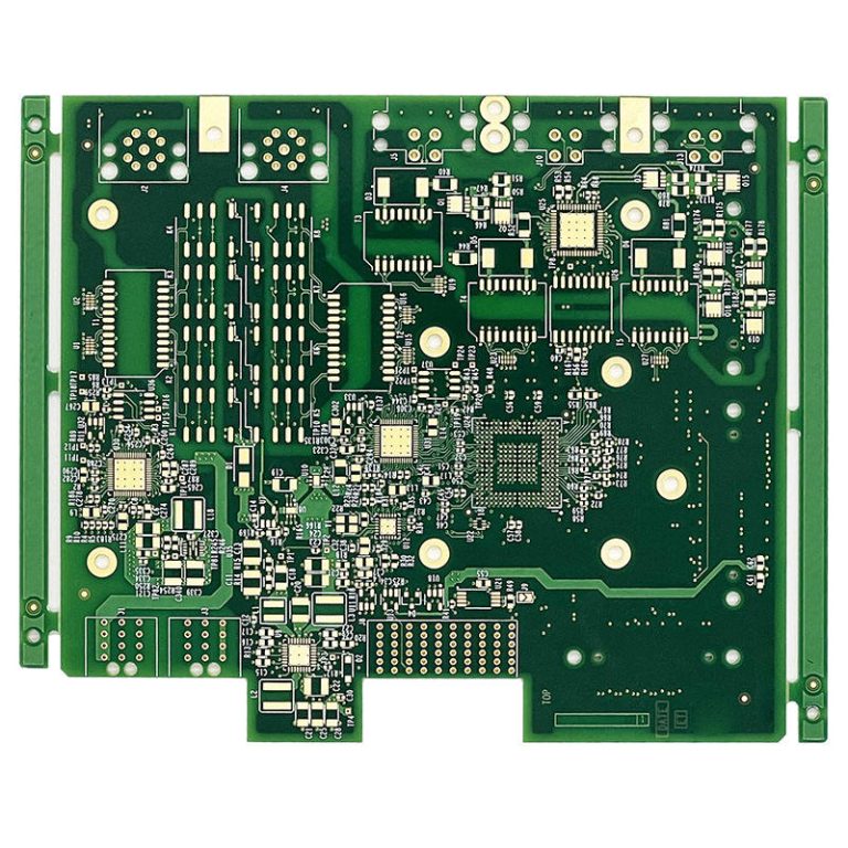
High-speed PCB design refers to layouts engineered to handle signals with rapid transitions and high frequencies. These designs are essential for applications requiring fast data processing and reliable signal transmission. Industry standards classify a PCB as high-speed when it operates at frequencies exceeding 1 GHz. Such designs often utilize materials with low dielectric constants to minimize signal loss and ensure optimal performance.
High-speed PCBs are integral to advanced technologies like 5G communication, radar systems, and satellite applications. Their ability to maintain signal integrity under demanding conditions makes them indispensable in modern telecommunications and data processing. Additionally, these designs often feature environmental suitability, such as low water absorption, which enhances their reliability in humid environments. However, specialized materials required for high-speed designs can increase production costs.
| Characteristic | Description |
|---|---|
| Operational Frequency | Designed to operate at frequencies above 1 GHz. |
| Material Properties | Features materials with low dielectric constants and minimal signal loss. |
| Applications | Critical for 5G communication, radar systems, and satellite technology. |
| Signal Integrity | Essential for fast and reliable signal transmission in modern telecommunications and data processing. |
| Environmental Suitability | Low water absorption makes them suitable for humid environments, though specialized materials increase costs. |
Key parameters: frequency, rise time, and data transfer rate
Three critical parameters define high-speed PCB design: frequency, rise time, and data transfer rate. Frequency determines the maximum operational speed of the PCB, with high-speed designs often exceeding 1 GHz. Rise time refers to the time it takes for a signal to transition from low to high voltage. Faster rise times demand precise impedance control to prevent signal distortion.
Data transfer rate, influenced by the Nyquist rate, represents the maximum data throughput achievable by the PCB. High-speed designs optimize this parameter by balancing bandwidth and the number of logic levels used in signal transmission. For example, differential blind vias connected to 100 Ohm pairs can achieve bandwidth limits of up to 70 GHz, ensuring efficient data handling.
| Parameter | Value | Description |
|---|---|---|
| Bandwidth Limit | 70 GHz | The channel bandwidth for differential blind vias connected to 100 Ohm pairs. |
| Return Loss Threshold | -10 dB | The frequency at which the return loss reaches -10 dB, indicating the bandwidth limit. |
| Data Rate Relation | Nyquist Rate | The relationship between bandwidth and data rate, influenced by the number of logic levels. |
Common challenges in high-speed PCB design
High-speed PCB design introduces several challenges that can compromise performance if not addressed properly. Signal integrity issues, such as impedance mismatches, often lead to signal reflection and distortion. Designers must carefully manage transmission line impedance to mitigate these effects.
Electromagnetic interference (EMI) poses another significant challenge. High-speed signals generate electromagnetic fields that can interfere with nearby components, causing data errors or system malfunctions. Proper shielding and grounding techniques are essential to minimize EMI.
Crosstalk, the unwanted coupling of signals between adjacent traces, can degrade signal quality in high-speed designs. Designers often use spacing and routing strategies to reduce this effect. Additionally, achieving the maximum frequency and maximum data transfer rate requires precise material selection and adherence to design guidelines, which can increase complexity and production costs.
Tip: To overcome these challenges, designers should prioritize signal integrity, leverage simulation tools, and follow industry best practices for layout and routing.
Principles of Signal Integrity in High-Speed Design
What is signal integrity, and why is it critical?
Signal integrity refers to the ability of a high-speed PCB to transmit reliable signals without distortion, reflection, or loss. It ensures that data reaches its destination accurately, maintaining the performance of digital communication systems. As devices operate at higher speeds, maintaining signal integrity becomes increasingly challenging due to factors like timing skews, crosstalk, and path loss. These issues can lead to data errors, reduced performance, or even system failure.
Several factors influence signal integrity in high-speed PCB design. Impedance mismatches, for instance, can cause signal reflection, while poor via design and inadequate ground plane strategies can degrade signal quality. Industry surveys highlight the importance of signal integrity in preventing communication errors, especially as miniaturization and high-performance demands grow. Designers must adopt mitigation strategies such as proper termination, impedance matching, and optimized layout techniques to address these challenges effectively.
Note: Signal integrity is not just a technical requirement but a cornerstone of reliable high-speed PCB design. Without it, achieving consistent performance in modern electronics becomes nearly impossible.
The role of impedance matching in preventing signal reflection and distortion
Impedance matching plays a pivotal role in maintaining signal integrity by minimizing signal reflection and distortion. When the impedance of a transmission line matches the source and load, signals travel smoothly without bouncing back or losing energy. This alignment ensures that high-speed circuits can transmit data efficiently, even at higher frequencies.
Quantitative studies, such as those referenced in Altera Application Note AN529, demonstrate the benefits of proper impedance matching. For example, controlled impedance in transmission line design can significantly reduce signal reflection, enhancing overall performance. Designers often use termination techniques, such as series or parallel termination, to achieve impedance matching. These methods help maintain signal quality by absorbing excess energy and preventing reflections.
Tip: Always calculate the characteristic impedance of your transmission lines during the design phase. This proactive approach ensures compatibility with the source and load, reducing the risk of signal degradation.
Transmission line design and controlled impedance
Transmission line design is a critical aspect of high-speed PCB layouts. It involves creating pathways that guide signals from one component to another while preserving their integrity. Controlled impedance is a key parameter in this process, as it ensures that the transmission line maintains a consistent impedance value throughout its length. This consistency prevents signal distortion and reflection, which are common in high-speed designs.
Designers achieve controlled impedance by carefully selecting trace width, spacing, and dielectric material properties. For instance, microstrip and stripline configurations are popular choices for maintaining controlled impedance in high-speed PCBs. These structures provide predictable electrical characteristics, making them ideal for applications requiring reliable signals.
The importance of transmission line design extends beyond impedance control. Proper routing strategies, such as minimizing trace lengths and avoiding sharp bends, further enhance signal integrity. Additionally, simulation tools can validate the design, allowing engineers to identify and resolve potential issues before manufacturing.
Callout: Controlled impedance and transmission line design are inseparable in high-speed PCB design. Together, they form the foundation for achieving reliable, distortion-free signal transmission.
PCB Design Guidelines for High-Speed Layouts
Material selection for high-speed PCBs
Selecting the right materials is critical for ensuring optimal performance in high-speed PCB designs. Materials with low dielectric constants (Dk) and dissipation factors (Df) are preferred, as they minimize signal loss and maintain signal integrity. For instance, a Dk value below 4 and a Df of 0.005 or less are ideal for high-speed applications. These properties reduce insertion loss and improve overall performance at higher frequencies.
The following table highlights key metrics to consider when choosing high-speed PCB materials:
| Metric | Description |
|---|---|
| Dielectric Constant | Affects impedance and signal integrity; lower values are preferred for high-speed applications. |
| Dissipation Factor | Indicates energy absorption; lower values (0.005 or less) are better for minimizing insertion loss. |
| Dispersion | Refers to changes in dielectric constant with frequency; minimal dispersion is ideal for signal integrity. |
| Insertion Loss | Higher for materials with poor dissipation factors; critical for maintaining signal quality at high speeds. |
| Signal Integrity | Maintained by selecting materials with stable dielectric constants and low losses. |
High-speed PCB materials like FR-4, Rogers 4350B, and Taconic RF-35 are commonly used due to their favorable electrical properties. However, designers must balance performance with cost, as advanced materials can significantly increase production expenses.
Component placement and routing strategies
Proper component placement and routing are essential for achieving reliable high-speed board layouts. Designers should prioritize placing critical components, such as signal pathways and power distribution elements, before arranging secondary components. Short and straight traces for high-speed signals help reduce signal degradation and improve performance.
Best practices for component placement and routing include:
- Place critical components first, including signal pathways and power distribution.
- Use short and direct traces to minimize signal distortion.
- Optimize signal tracing geometry to reduce interconnection resistance.
Organizations like NASA emphasize the importance of controlled impedance and solid return paths, while manufacturers such as ProtoExpress recommend using low-Df materials and tight impedance control. PCBWay advises isolating RF zones and employing direct traces to enhance signal quality. Learning from these insights helps engineers avoid common pitfalls and improve design effectiveness.
Termination techniques to reduce signal distortion
Termination techniques play a vital role in reducing signal distortion in high-speed PCB designs. Proper termination prevents signal reflection by matching the impedance of the transmission line with the source and load. Common methods include series termination, parallel termination, and Thevenin termination.
- Series termination involves placing a resistor in series with the signal line near the source. This method absorbs excess energy and prevents reflections.
- Parallel termination uses a resistor connected between the signal line and ground at the load end, ensuring impedance matching.
- Thevenin termination combines two resistors to create a voltage divider, offering a balanced approach for impedance control.
Each technique has its advantages and is selected based on the specific requirements of the high-speed layout. Implementing these methods ensures reliable signal transmission and minimizes distortion, even at higher frequencies.
Tip: Always validate termination techniques using simulation tools to ensure compatibility with the high-speed PCB design.
Advanced Techniques for High-Speed PCB Optimization
HDI PCB design and its advantages
High-Density Interconnect (HDI) PCBs have revolutionized modern electronics by enabling compact, high-performance designs. These PCBs utilize advanced manufacturing techniques to achieve smaller form factors while maintaining superior electrical performance. Industries such as healthcare, automotive, and military rely on HDI technology to meet stringent space and performance requirements.
HDI PCBs offer several advantages:
- Enhanced signal integrity ensures reliable performance in high-frequency applications.
- Smaller and lighter devices become achievable through miniaturization.
- Higher component density allows for increased functionality in limited spaces.
| Advantage | Description |
|---|---|
| More Interconnections | HDI PCBs allow for more interconnections in smaller areas, facilitating miniaturization. |
| Smaller Form Factors | The design enables the creation of smaller and denser boards, essential for compact devices. |
| Higher Component Count | HDI technology supports a higher component count, enhancing functionality in limited space. |
| Improved Signal Integrity | Ensures minimal loss or distortion of electronic signals, crucial for high-frequency applications. |
| Enhanced Electrical Performance | Contributes to the overall reliability and performance of electronic systems. |
These benefits make HDI PCBs indispensable for applications requiring compact and efficient designs.
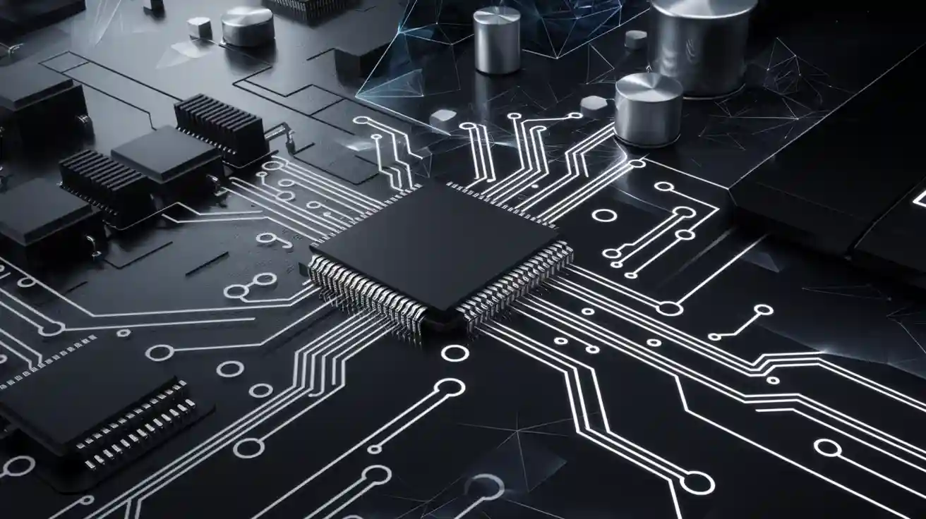
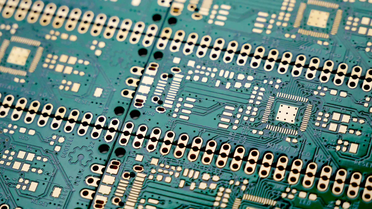
Best practices for via transitions in RF PCB layouts
Via transitions play a critical role in maintaining signal integrity in RF PCB layouts. Poorly designed vias can introduce signal losses, reflections, and impedance mismatches, especially at high frequencies. Designers must adopt best practices to optimize via performance.
Key recommendations include:
- Use micro vias instead of traditional plated-through-hole vias to eliminate stubs and improve bandwidth.
- Place stitching vias around signal vias to maintain a consistent impedance of 50 Ohms across frequencies.
- Employ via-in-pad plated over (VIPPO) techniques with laser-drilled vias to ensure all transmission occurs on the desired layer.
Careful placement of vias minimizes return loss and insertion loss, ensuring optimal performance in high-speed designs. These practices are essential for achieving reliable signal transmission in GHz-range applications.
Leveraging simulation tools for design validation
Simulation tools have become indispensable for validating high-speed PCB designs. These tools allow engineers to identify potential issues early in the design process, reducing errors and iterations. Advanced simulation capabilities enable precise modeling of signal behavior, ensuring optimal performance.
| Success Metric | Description |
|---|---|
| Accelerating Time-to-Market | Reduced design cycles, enabling faster delivery of multiple high-speed PCBs to clients. |
| Improved Design Accuracy | Early problem detection and advanced simulation capabilities minimize errors and iterations. |
| Optimized Costs | Decoupling capacitor optimization and power layer reductions save materials and design resources. |
| Enhanced Reputation and Client Confidence | Solidified ALS’s position as a trusted partner for high-speed PCB projects. |
By leveraging these tools, designers can optimize layouts, validate impedance control, and ensure compliance with industry standards. Simulation tools not only enhance design accuracy but also accelerate time-to-market, making them a cornerstone of modern PCB development.
Tools and Resources for High-Speed PCB Design
PCB design software for advanced layouts
Modern PCB design software offers powerful tools for creating advanced layouts tailored to high-speed applications. These platforms integrate features like schematic capture, PCB layout, and simulation capabilities, enabling designers to optimize signal integrity and minimize errors. The market includes a diverse range of solutions, from entry-level tools to enterprise-grade suites. Cloud-based platforms and AI-driven design assistance are becoming increasingly popular, enhancing collaboration and efficiency in complex projects.
Key software options include:
- Altium Designer: Known for its robust simulation tools and user-friendly interface.
- Cadence Allegro: Offers advanced routing capabilities and controlled impedance features.
- Mentor Graphics Xpedition: Provides AI-driven design assistance for high-speed layouts.
- KiCad: A free, open-source solution suitable for smaller projects.
- Zuken CR-8000: Ideal for multi-board designs and enterprise-level applications.
A comparative analysis of these tools highlights their strengths in handling high-speed designs. For instance, Altium Designer excels in schematic capture, while Cadence Allegro offers superior routing for complex layouts. Designers can leverage tutorials and guides to evaluate software performance in practical scenarios, ensuring the best fit for their project needs.
Tip: Choose software that aligns with project complexity and team collaboration requirements to maximize efficiency.
Educational resources: webinars and design guides
Educational resources play a vital role in equipping designers with the knowledge needed for high-speed PCB design. Webinars hosted by industry leaders provide insights into emerging trends, best practices, and advanced techniques. Design guides offer step-by-step instructions for optimizing layouts, ensuring signal integrity, and adhering to manufacturing standards.
Recommended resources include:
- Webinars: Platforms like PCBWay and ProtoExpress regularly host sessions on topics such as controlled impedance and HDI design.
- Design Guides: IPC standards and manufacturer-specific guides, such as those from Rogers Corporation, provide detailed instructions for material selection and routing strategies.
- Online Courses: Websites like Udemy and Coursera offer courses on PCB design fundamentals and advanced techniques.
These resources help designers stay updated on industry advancements and refine their skills. By participating in webinars and studying design guides, engineers can reduce design time and improve the reliability of high-speed layouts.
Callout: Continuous learning through webinars and guides ensures designers remain competitive in the rapidly evolving PCB industry.
Certifications and compliance for quality assurance
Certifications and compliance standards ensure the quality and reliability of high-speed PCB designs. Industry standards like IPC-A-610 define accepted practices for PCB assembly, while ISO certifications improve communication and efficiency during production. RoHS compliance promotes environmentally responsible manufacturing by restricting hazardous substances.
Key certifications include:
- IPC Standards: Ensure consistent quality and safety in PCB manufacturing.
- ISO 9001:2015: Indicates adherence to quality management principles.
- RoHS Compliance: Guarantees environmental safety by limiting hazardous materials.
- UL Listing: Provides assurance of product safety and performance.
- MIL Standards: Essential for military-grade PCB applications.
Additional practices, such as Automated Optical Inspection (AOI) and Time Domain Reflectometer (TDR) testing, further enhance quality assurance. These measures verify electrical integrity and detect defects during manufacturing, ensuring zero-defect boards.
Note: Adhering to certifications and compliance standards not only ensures product reliability but also builds trust with clients and stakeholders.
Optimizing high-speed PCB design requires a strategic approach to ensure reliable performance. Designers must prioritize signal integrity by addressing factors like impedance mismatches, electromagnetic interference, and crosstalk. Key practices include maintaining equal trace lengths for differential pairs, using controlled impedance routing, and avoiding right angles to reduce reflections. Specifying core and prepreg thicknesses further enhances characteristic impedance control, while higher-quality materials improve overall performance.
A full ground plane mitigates electromagnetic interference and reduces inductance, ensuring low impedance. Routing signal traces effectively and separating high-speed signals from low-speed ones minimizes signal loss and distortion. These techniques not only enhance design accuracy but also reduce development time, enabling faster delivery of high-speed solutions.
Exploring advanced tools and resources, such as webinars, design guides, and simulation software, empowers designers to refine their skills and stay ahead in the rapidly evolving PCB industry. Continuous learning and adherence to best practices pave the way for innovation and excellence in high-speed PCB design.
FAQ
What is the most effective way to reduce design time for high-speed PCBs?
Using simulation tools early in the design process minimizes errors and iterations. These tools validate impedance control, signal integrity, and layout efficiency. Designers can also adopt modular design practices, reusing proven circuit blocks to accelerate development without compromising quality.
How can designers minimize electromagnetic interference (EMI) in high-speed PCBs?
Designers should implement a full ground plane to reduce EMI. Proper shielding, controlled impedance routing, and separating high-speed signals from low-speed ones also help. Additionally, avoiding sharp trace bends and maintaining consistent trace widths improve EMI performance.
Why is controlled impedance critical in high-speed PCB design?
Controlled impedance ensures consistent signal transmission by preventing reflection and distortion. It maintains signal integrity, especially at higher frequencies. Designers achieve this by carefully selecting trace width, spacing, and dielectric material properties during the layout phase.
What are the benefits of using HDI technology in high-speed PCBs?
HDI technology enables compact designs with higher component density. It improves signal integrity and electrical performance, making it ideal for applications requiring miniaturization. Industries like automotive and healthcare rely on HDI for space-constrained, high-performance devices.
Which materials are best for high-speed PCB applications?
Materials with low dielectric constants (Dk) and dissipation factors (Df) are ideal. Options like Rogers 4350B and Taconic RF-35 minimize signal loss and maintain integrity. Designers should balance performance with cost when selecting materials for specific applications.