Guidelines for Efficient and Reliable Multilayer PCB Design

You can make multilayer pcb design work well by planning the stack-up carefully. You should pick smart materials and follow strict design rules. If you use best practices, your printed circuit board gets smaller. It also lets you change the design more easily. It can handle high-speed uses. This way, you get better performance. You also save money on multilayer projects.
| Benefit | Description |
|---|---|
| Compact Size and Space Efficiency | Puts many circuit layers in a small space. This is good for tiny devices. |
| Enhanced Performance | Makes signals better and cuts down on electromagnetic problems. This helps keep electrical work steady. |
| High-Speed Capabilities | Works for fast uses by keeping signals strong and steady. |
| Greater Design Flexibility | Gives more ways to route circuits. You can make harder designs and fit more parts. |
| Cost-Effectiveness in Production | Saves money when making a lot because you need fewer parts and there are fewer mistakes. |
Key Takeaways
- Think about your multilayer PCB stack-up before you start. This helps make it smaller and work better.
- Try to use the least number of layers you can. This saves money and keeps signals strong.
- Pick materials that fit what your design needs. This helps with heat and keeps signals clear.
- Use controlled impedance routing in your design. This stops signals from getting lost when they move fast.
- Follow rules for making your design easy to build. This helps more boards work right and lowers mistakes.
Multilayer PCB Stack-Up Guidelines
Minimizing Layer Count
You should always try to use the fewest layers possible in your multi-layer pcb. Fewer layers make your multilayer pcb design less expensive and easier to build. When you use fewer layers, you also reduce the number of vias. This helps keep your signal integrity strong because there are fewer places for signals to get lost or distorted.
💡 Tip: Start by estimating how many layers you need based on your circuit’s complexity and speed. If your design is simple, you may only need four layers. For more complex or high-speed multilayer stack-up design, you might need six or more layers.
Here are some ways you can decide the best number of layers for your multi-layer pcb:
- Look at your circuit’s routing needs. If you have many connections, you may need more layers.
- Think about the types of signals you have. High-speed signals often need extra layers for better control.
- Check your power and ground needs. More power and ground planes can help with signal integrity.
- Use simulation tools to test your layer stackup strategy before you finish your design.
- Try to keep the stack-up symmetrical. This helps prevent warping during manufacturing.
You must balance cost and performance. If you use too few layers, your board may not work well for high-speed signals. If you use too many, your costs go up.
Layer Arrangement for Signal and Power
How you arrange your layers in a multi-layer pcb matters a lot. Good layer arrangement helps your multilayer pcb work better and last longer. You want to keep signal layers close to ground planes. This gives signals a clear path to return, which keeps your signal integrity high and cuts down on noise.
- Place critical signals in inner layers. Put ground planes above and below these layers.
- Overlap power and ground planes. This helps spread power evenly and keeps signals clean.
- Keep your stack-up symmetrical. This stops your printed circuit board from bending or twisting.
- Use ground planes to lower electromagnetic interference (EMI). This makes your multi-layer pcb safer and more reliable.
🛠️ Note: Good circuit board stackups use impedance control. This means you match the resistance of your traces to the needs of your signals. You can use special tools to check this during your design.
When you follow these steps, you make your multi-layer pcb design strong and ready for high-speed uses.
Common Stack-Up Mistakes
You can avoid many problems by watching out for common mistakes in multilayer pcb design. Here are some errors you should look for:
- Putting layers in the wrong order. This can cause signal integrity problems and more EMI.
- Using the wrong layer thickness. This can mess up impedance and hurt performance.
- Not leaving enough space between layers. This can cause short circuits and other issues.
- Picking the wrong materials. This can make your multi-layer pcb fail, especially at high speeds.
- Not talking to your manufacturer. This can lead to mistakes in your layer stackup.
- Forgetting about mechanical needs. This can make your board hard to assemble or less reliable.
- Ignoring heat management. This can make parts overheat and fail.
⚠️ Alert: If you do not balance your layers, your board can warp or twist. This can cause your multi-layer pcb to break or not work right.
You should always check your design requirements and talk with your manufacturer before you finish your multi-layer pcb. This helps you avoid costly mistakes and keeps your performance high.
Material Selection for Multi-Layer PCB
Standard vs. Advanced Materials
You have to pick the right laminate for your multilayer pcb. Most people use FR-4 as the usual material. FR-4 works for many printed circuit board jobs. It has a glass transition temperature (Tg) of about 180℃. It gives okay thermal stability. If you want better results, you can choose advanced materials. These materials have higher Tg and better thermal stability. They help your multilayer pcb design work well at high speeds.
| Material | Glass Transition Temperature (Tg) | Thermal Stability |
|---|---|---|
| FR-4 | ~180℃ | Moderate |
| Advanced | Higher than FR-4 | High |
- FR-4 has a dielectric constant between 4.2 and 4.8. Its dissipation factor is about 0.02. This can cause signal loss in high-frequency uses.
- Advanced laminates have lower dissipation factors and more stable dielectric constants. They keep signals strong and clear.
If your multilayer pcb needs to handle signals above 1 GHz, advanced laminates will give you better signal integrity.
IPC and Industry Standards
You should always check IPC standards when you pick materials for your multilayer pcb. These standards help you make sure your design meets industry rules for safety and quality.
- IPC-4101 sets the main rules for rigid and multilayer pcb laminate selection. It helps you get the same quality from different suppliers.
- IPC-4103 focuses on high-speed laminates. You need this for RF, microwave, and digital circuits.
- IPC-4202 covers flexible dielectric materials. You use these for multilayer designs that need to bend or move.
📝 Tip: Following IPC standards helps you avoid problems with performance and reliability.
Cost and Availability Factors
You must think about cost and supply when you choose a laminate for your multilayer pcb. FR-4 is easy to find and costs about $0.10 to $0.50 per square inch. Rogers materials can cost $20.00 to $75.00 per square inch. Ceramic substrates range from $2.00 to $10.00 per square inch. High-frequency laminates can cost over $1.00 per square inch. Thicker copper in your design can raise costs by 20-30%.
- FR-4 is the most affordable and widely available.
- Advanced laminates need special equipment to make. This can limit supply and raise prices.
- Multilayer pcb production takes more time and is more complex than single-layer boards.
You should balance your design needs, performance goals, and budget before you pick a laminate.
High-Speed PCB Design and Signal Integrity
Controlled Impedance Routing
You need to think about controlled impedance in high-speed pcb design. This keeps signal integrity strong and stops problems like reflections or signal loss. Impedance matching for parts and traces is important. You must watch trace geometry because it changes the characteristic impedance. You should also pick PCB materials with a low dielectric constant and low loss tangent to help signals work better.
Here are steps for controlled impedance:
- Work with your manufacturer to pick materials that fit your impedance needs and have even thickness.
- Set trace geometry carefully to keep the right impedance.
- Keep a ground plane under high-speed signal layers. This helps stabilize impedance and lowers electromagnetic interference.
- Control trace length and routing to lower unwanted inductance and capacitance.
💡 Tip: Controlled impedance routing is very important for high-speed design. It helps you stop signal integrity problems in your multilayer pcb.
Reducing Crosstalk and EMI
You can lower crosstalk and electromagnetic interference by using smart layout tricks in your multilayer pcb. Wide and steady ground planes help shrink loop areas and cut EMI. You should leave enough space between signal traces and use differential pairs for high-speed signals. This lowers crosstalk.
- Put high-speed and low-speed signals far apart to lower noise.
- Place decoupling capacitors close to IC power pins to block noise.
- Use metal boxes or grounding strips if you need more shielding.
⚡ Note: Good trace routing and placing parts protect your printed circuit board from extra noise.
Power Distribution Network
A strong power distribution network helps both power integrity and signal integrity in high-speed pcb design. You should use many vias for high-current paths. Put these vias close to component pins to keep voltage steady. Spread vias evenly across power planes for even current flow. Shorter vias lower inductance, which helps power integrity.
- Pair power and ground layers to make low-impedance paths.
- Keep power layers next to ground layers to lower noise.
- Add decoupling capacitors near vias to keep voltage steady and cut noise.
- Make your layer stack-up better to help power delivery and signal integrity.
🛠️ Tip: Careful planning of power distribution in multilayer pcb design gives you better performance and reliability in high-speed design.
Component Placement and Thermal Management
Placement for Performance and Accessibility
You can make your multilayer pcb work better by putting parts in smart places. Good placement helps your board last longer. First, make a plan for where each part will go. This plan gives space for every circuit and connector. Put power parts together to lower signal problems. Keep high-speed signal paths short. Short paths help your design work faster and lose less signal.
- Put analog and digital circuits in different spots to stop crosstalk.
- Check voltage and current, then group similar circuits.
- Do not let high-speed lines cross splits in power planes.
- Keep sensitive high-speed devices away from the edges. This lowers electromagnetic interference.
- Make sure hot parts have open airflow to cool down.
You should always make test points and connectors easy to reach. Easy access helps with repairs and upgrades.
Thermal Vias and Heat Dissipation
Thermal management is important for strong electronics. You need to move heat away from hot spots. This keeps your multilayer design safe. Put thermal vias near hot parts. These vias let heat travel to cooler spots or heat sinks. This stops heat from building up and keeps your board safe.
Add heat sinks to give heat more room to escape. Use thermal interface materials to help heat move from parts to heat sinks. Good placement of these materials keeps your system safe and steady.
Preventing Board Warpage
You can stop warping in multilayer boards by using smart steps.
- Balance copper and dielectric layers to keep the stackup even.
- Pick high-Tg materials to help your board stay flat.
- Pre-bake bare boards to get rid of moisture and lower delamination risk.
- Use strong rails during panelization for extra support.
- Control the reflow profile to manage temperature changes.
- Support the board across the pallet to stop sagging.
- Use low spring force when holding the board edges.
- Balance copper on all layers to lower expansion differences.
- Pick substrates with close expansion rates.
- Keep copper density even between rails and the board.
If you follow these steps, your high-performance designs will stay flat and work well.
PCB Design Guidelines for Manufacturability
You should follow pcb design guidelines to make your multilayer pcb easy to build. Good planning helps you avoid mistakes and delays. Think about how your choices affect making the board and how long it will last.
Copper Weight and Line Spacing
Copper weight and line spacing are important in pcb design guidelines. If you use thicker copper, you need wider traces. You also need more space between traces. This keeps your board safe from shorts. It also lets your board carry more current. The table below shows the smallest space and trace width for each copper weight:
| Copper Weight | Minimum Recommended Space (mil) | Minimum Trace Width (mil) |
|---|---|---|
| 1oz | 3.5 | 3.5 |
| 2oz | 8 | 8 |
| 3oz | 10 | 10 |
| 4oz | 14 | 14 |
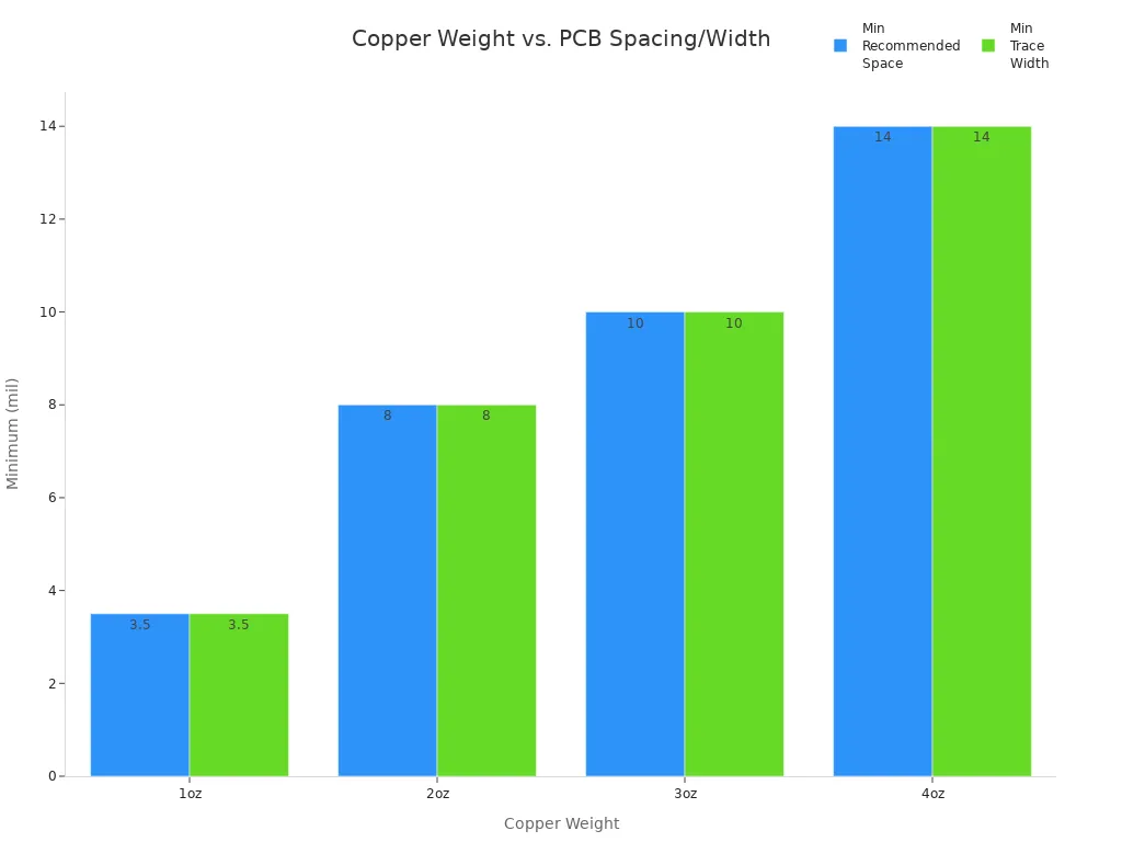
If you follow these pcb design guidelines, you lower the chance of shorts. You also make your board work better.
Drilling and Mechanical Tolerances
Drilling and mechanical tolerances are important in pcb design guidelines. You must control hole sizes and trace widths. Good tolerance management helps you avoid defects. It keeps your board working well. If you do not manage tolerances, you can get bad solder joints or broken connections.
| Aspect | Impact on Yield and Reliability |
|---|---|
| Tolerance Management | Makes sure production is good and electrical work is steady. |
| Mismanagement Consequences | Can cause problems in making, performance, and assembly. |
| Trace Width Control | Needed to stop defects in electrical paths and keep reliability. |
| Solder Joint Reliability | Tolerance levels can cause stress or tombstoning in parts. |
| Production Yield Improvement | Good tolerance control can raise production yield and lower costs. |
- Plated-through holes must be good for strong boards.
- Bad hole walls can cause failures and delamination.
- High aspect ratios make plating harder and can hurt performance.
Solderability and Assembly Yield
You can make soldering and assembly better by following pcb design guidelines. Use fresh solder paste and keep it at the right temperature. Check your equipment often to keep it working well. Train your team so they know how to build boards the best way.
- Use design for manufacturability to stop problems.
- Leave enough space between parts for machines.
- Follow IPC standards to avoid common mistakes.
- Pick good parts and materials for better reliability.
- Test your boards to find and fix problems early.
- Make pad sizes right for strong solder joints.
- Put parts in the same direction to help machines and checks.
If you use these pcb design guidelines, you make your multilayer boards easier to build and more reliable.
Advanced Interconnects in Multilayer PCB
Through-Hole, Blind, and Buried Vias
You can link layers in a multilayer board with different vias. Through-hole vias go from the top to the bottom. Blind vias connect an outside layer to inside layers but do not go all the way through. Buried vias only connect inside layers and cannot be seen from outside. Each via type has good points and some limits.
| Via Type | Advantages | Limitations |
|---|---|---|
| Blind Vias | 1. More routing options 2. Better signal quality 3. Flexible design 4. Lower making costs |
1. Harder to make 2. Limits on layer number |
| Buried Vias | 1. Better signal quality 2. Less EMI 3. Saves board space 4. Flexible design |
1. Harder to make 2. Hard to reach |
Blind vias are used in phones, fast digital boards, and space systems. Buried vias are good for boards with lots of connections and tough designs.
Microvias and HDI
Microvias change how you build high-density boards. You use microvias to fit more connections in less space. Microvias help you add more features to phones, watches, and medical tools. Cars use microvias for small radar and camera parts.
Microvias make PCBs work better. They give signals a shorter path. This keeps signals strong and stops them from getting weak. It is very important for fast digital signals. Even small losses can hurt how things work.
Microvias and high-density boards give you three main benefits:
- More wiring in less space.
- Fewer layers mean lower cost and easier making.
- Better signal quality for fast circuits.
Microvias are found in almost every new high-density board. They help keep devices thin and powerful.
Via-in-Pad Techniques
Via-in-pad saves space in your multilayer board. You put microvias right under part pads. This works well for boards with tiny parts close together. Pick the right fill for your microvia based on heat and electricity needs. Pad size should fit the microvia and not mess up part placement. Plan your layers to get the most out of this method.
- Plug and cap microvias to stop solder from moving away.
- Make sure pads cover the microvia to stop solder spread.
- Use microvias to help move heat and keep impedance steady.
Follow these steps for best results:
- Keep microvia size between 0.2mm and 0.3mm. Make pad size at least 0.1mm to 0.15mm bigger.
- Fill or plug microvias to stop solder from moving.
- Cover open microvias with solder mask.
- Put microvias evenly under tiny parts.
Talk to your maker early. Use computer tools to check signals and heat. Test your boards before making many. Using microvias and high-density tricks makes your multilayer boards smaller, faster, and stronger.
Quality Control and Testing in Multilayer PCB Design
In-Process Inspection
You need strong quality control at every step. In-process inspection helps you find problems early. X-ray inspection lets you look inside the board without hurting it. You can see hidden problems like layers that do not line up, empty spots, or issues with vias. Automatic Optical Inspection (AOI) checks the board’s surface quickly. Manual visual inspection is cheap and fast for simple boards. But it can miss small problems. Automatic laser measurement gives exact data about solder paste. Sometimes, parts block the laser, so it does not always work.
| Inspection Method | Strengths | Weaknesses |
|---|---|---|
| Manual Visual Inspection (MVI) | Low cost, fast, good for small runs. | May miss defects, depends on operator skill. |
| Automatic Laser Measurement (ALT) | High precision, quick solder paste check. | Can be blocked by some components. |
| X-ray Inspection (AXI) | Finds hidden defects in dense boards. | High cost, not needed for simple boards. |
| Automatic Optical Inspection (AOI) | Fast, repeatable, good for mass production. | Cannot check inside solder joints, needs other methods. |
🛡️ Tip: Non-destructive inspection keeps your boards safe while you check for problems.
Electrical Testing
Quality control means you must test the electrical paths. You check for broken circuits and bad connections. You make sure every path works as it should. Basic electrical tests check voltage, current, and resistance. Signal integrity tests show how well signals move. Functional tests make sure all parts work together. Environmental tests check if your board works in hot or cold places.
- Find breaks in the circuit.
- Find bad connections.
- Make sure all paths work.
| Test Type | Purpose |
|---|---|
| Basic Electrical Tests | Measure voltage, current, and resistance for basic function. |
| Signal Integrity Tests | Check the quality of signals in the PCB. |
| Functional Tests | Make sure all parts connect and work. |
| Environmental Tests | Test performance in tough conditions. |
Documentation and Traceability
You need good records and traceability for strong quality control. You can use barcode labels, RFID tags, or marks on parts to track each board. Manufacturing Execution Systems (MES) save data about every step. You can link MES with other systems to keep records complete. Traceability can be for a batch, one board, or even each part.
- Barcode or QR code labels help you track boards.
- RFID tags let you scan boards fast.
- Marks on parts last for the board’s whole life.
- MES keeps all your data in one place.
- You can connect MES with ERP, PLM, and QMS for full traceability.
📋 Note: Good records and traceability help you fix problems fast and show your quality control meets industry rules.
Cost Optimization in Multilayer PCB Production
Design Choices Affecting Cost
You can save money in multilayer pcb production by making smart choices. Picking the right material changes the price of your printed circuit board. The number of layers affects how hard and costly your board is to make. Copper thickness matters too. Thicker copper costs more and takes longer to work with. If you do not plan your stackup well, it can make manufacturing harder and cost more.
Here are some mistakes that make costs go up:
- Choosing fancy materials when you do not need them.
- Adding layers you do not really need for your circuit.
- Using thick copper for traces that do not need much current.
- Making custom stackups that are hard to build.
- Not following design for manufacturability (DFM) tips.
💡 Tip: Match your design to your budget. Do not add things you do not need.
Panelization and Yield
Panelization lets you make many boards at the same time. You can put lots of small boards on one big panel. This makes production faster and lowers labor costs. Panelization also helps stop handling mistakes and keeps boards safe. Good panelization means you can process many boards together. This gives you more working boards and saves money.
- Panelization helps you make more boards quickly.
- It lowers mistakes and stress on each board.
- You get better results in manufacturing.
🛠️ Good panelization means you get more working boards for less money.
Supplier Collaboration
You can save money and time by working well with your suppliers. Strong partnerships help you get better prices and faster help. If you work with suppliers for a long time, you may get priority when supplies are low. Smart sourcing and good design choices help you cut costs but keep quality high.
| Best Practice | Description |
|---|---|
| Invest in Robust Supplier Relationships | Work with trusted manufacturers for long-term success. |
| Tips for Selection | Pick ISO-certified suppliers with good systems and quick lead times. |
| Facility Assessment | Visit or check the facility for cleanliness and rules. |
- Working closely with suppliers can make your production better.
- You get more help and can fix problems faster.
🤝 Good supplier teamwork helps you make strong, affordable multilayer boards.
You can make multilayer pcb design work better by using these tips. First, keep enough space between traces. Pick trace widths that fit the current. Check drill and via sizes so making the board is easy. Keep copper away from the edges of the board. Control impedance to keep signals strong. If you put parts in smart places and use clear labels, you save money and make your product better. You can learn more by joining groups like IEEE and IPC. Reading magazines about the industry helps you stay up to date.
FAQ
What is the main benefit of using multilayer PCBs?
You get more space for circuits in a smaller board. This lets you build powerful devices that fit in your hand. Multilayer PCBs also help signals move faster and stay strong.
How do you choose the right number of layers?
You look at your circuit’s needs. If you have many connections or high-speed signals, you add more layers. Use design tools to test your stack-up before you decide.
Why do you need controlled impedance in high-speed designs?
Controlled impedance keeps signals clear and steady. If you match the impedance, you stop signal loss and reflections. This helps your board work well at fast speeds.
What is the difference between blind and buried vias?
| Via Type | Where It Connects | Can You See It? |
|---|---|---|
| Blind | Outside to inside layers | Yes |
| Buried | Only inside layers | No |
Blind vias connect outer and inner layers. Buried vias link only inner layers.
How can you prevent PCB warping during manufacturing?
🛡️ Tip: Balance copper on all layers. Use high-Tg materials. Pre-bake boards to remove moisture. Support boards during heating. These steps keep your PCB flat and strong.