Emerging Innovations in PCB Design and Layout for 2026

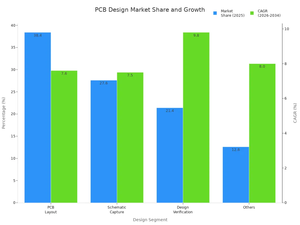
You see fast changes in PCB design & layout. These changes help electronics get better. Industry numbers say PCB design & layout has a 38.4% market share in 2025. It is expected to grow at 7.6% each year until 2034.
| Metric | PCB Design & Layout | Schematic Capture | Design Verification | Others |
|---|---|---|---|---|
| Market Share (2025) | 38.4% | 27.6% | 21.4% | 12.6% |
| CAGR (2026-2034) | 7.6% | 7.5% | 9.8% | 8.0% |
AI, high-speed computing, and new materials are making things change. You need to know about these trends. This will help you keep up with tighter impedance control, more layers, and new ways to make things.
Key Takeaways
- Keep learning about new trends like green manufacturing and AI tools. These can help make your PCB designs better. – Use advanced materials for high-speed uses. This helps signals stay clear and keeps things cooler. – Use automation in assembly and testing. This makes work faster and helps stop mistakes in making PCBs. – Try flexible PCB designs for wearables. This lets you make smaller and stronger devices that people want. – Pay attention to rules and eco-friendly ways. This keeps your PCB making safe and good for the planet.
Industry Trends in PCB Design & Layout
You see new trends changing printed circuit boards. These trends make electronics smarter, faster, and more reliable. You need to know how these changes affect design and manufacturing. They also change how you use technology.
Note: The table below lists the biggest trends for 2026. Each trend brings new problems and chances for you in pcb design & layout.
| Trend | Description |
|---|---|
| Green Manufacturing Practices | Makers use eco-friendly ways because of strict rules in the EU and North America. |
| Complexity in Design | You need smart tools like AI to handle harder designs and layouts. |
| Demand for Specialized PCBs | Areas like cars and AI need special printed circuit boards. |
| Supply Chain Strategies | Companies use a ‘China Plus One’ plan to lower risks in their supply chains. |
Higher Component Density
Devices keep getting smaller and stronger. Higher component density lets you put more features in a small space. This is important for high-performance computing and new medical devices. There are good things, but also new problems:
- You make devices with more power and features in less space.
- You help many industries use advanced electronics.
- You must fix heat problems because packed parts get hot.
- You need to plan well to connect parts, which makes building harder and can cause mistakes.
You have to use complex stack-ups and better cooling to keep things working. You also need to check your designs for problems before making them.
Mixed Technology Assemblies
You often mix different parts to get the best results. Mixed technology assemblies use both through-hole and surface mount parts. This way gives you many benefits:
- You get better performance by picking the right part for each job.
- You make production faster with machines, which saves money.
- You have more choices for parts in different uses.
- You make things more reliable by using both types of technology.
You must think about design for manufacturability (DFM). Placing parts carefully helps you avoid problems when putting things together. You also save time and make assembly easier by using fewer parts.
Global Supply Chain Shifts
You see big changes in where companies make printed circuit boards. Many makers move to Southeast Asia for cheaper work and better tariffs. Companies like Zhongfu Circuit build new factories in Thailand. China also makes more of its own high-end materials, reaching 58% for copper-clad laminates.
You need to change how you get your parts to keep up. You might pick local suppliers or use more than one source to lower risks. These changes help you stay strong and react fast to what the market wants.
Tip: Keep up with global trends. They can change your design choices, materials, and delivery times.
You see that trends like making things smaller, faster product changes, and new tech like IoT, AI, and 5G push you to make harder designs. You use advanced tools and software to keep up. Getting help from outside and using special design services helps you finish on time and make good products.
AI and Automation in PCB Manufacturing
AI-Driven Design Tools
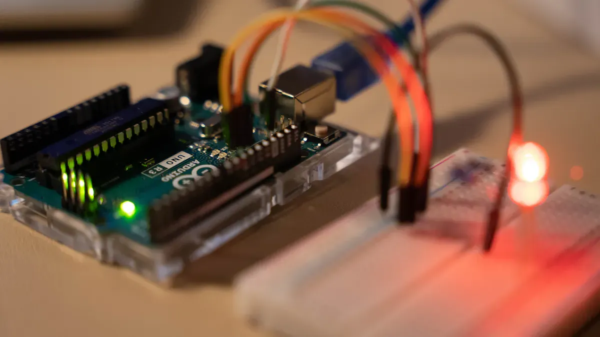
You can use AI-powered design tools now. These tools help you work faster and make fewer mistakes. Machine learning helps pick the best spots for parts and paths for wires. Here is how AI helps you: It suggests good places for parts and wires by looking at old designs. It checks your work for mistakes and tells you fast if there are problems. It remembers what you did before and gets better at helping you next time. It can test your PCB designs in many ways, so you find problems early. Your CAD tools get better with layout help and automatic paperwork. You get quick feedback on changes, so you can try new ideas without worry. With these tools, you do not have to do as many boring jobs. You can spend more time thinking of new ideas.
Automated Assembly and Testing
Automation changes how you put together and check PCBs. Machines build and check boards very fast and do not make many mistakes. You get some good things from this: You pay less for workers and do not waste as much material. Each board is made better and has fewer problems. Machines can find mistakes early with special cameras and x-rays. They can work all the time, so making boards does not slow down.
Here is a table that shows how automated and manual assembly are different:
| Aspect | Automated Assembly | Manual Assembly |
|---|---|---|
| Production Speed | Very high, runs non-stop | Slower, depends on workers |
| Quality Consistency | Low defects, high precision | Varies, depends on skill |
| Cost Efficiency | Lower cost for large batches | Higher cost for big orders |
| Flexibility | Best for mass production | Best for small runs and prototypes |
You see that using machines makes boards faster and better.
Simulation and Layout Optimization
Simulation and layout optimization tools help you fix hard design problems before you build anything. You use these tools to keep signals clear by changing wire lengths and paths for fast signals. You can make power better by finding and fixing spots with too much current. You also check for electromagnetic interference early to follow EMC rules. These tools let you fix problems before they cost a lot of money. You can make better boards, faster, and with fewer surprises.
High-Speed Computing and Advanced Materials
You notice big changes in PCB design from high-speed computing. You need new materials and better designs for faster data. Smaller devices also need these changes. These updates help you fix problems with signal quality and heat.
High-Frequency, Low-Loss Substrates
Special materials are needed for high-speed computing. These materials help signals move fast and stay clear. Check the table below for some new advancements:
| Advancement | Description |
|---|---|
| New Materials | M7-grade and BMI resin give better performance for high-speed applications. |
| Improved Manufacturing | New ways to make substrates lower costs and improve quality. |
| Policy Support | Governments give money for research on low-loss materials, which helps 5G technology grow. |
| Nano-zinc oxide Technology | This technology lowers signal loss and keeps signals strong. |
You use these materials to keep signals strong and cut down errors.
5G and IoT Integration
You must pick the right materials for 5G and IoT devices. Some materials work well at low frequencies. You need better ones for higher speeds.
- FR-4 works for IoT at 2.4 GHz, but not for 5G.
- Rogers RT/duroid 5880 is better for 5G at higher frequencies.
- Advanced materials cost more but give better performance.
- 5G gives you faster data, more capacity, and less delay.
- Millimeter-wave frequencies need careful design for good results.
| Material Type | Frequency Range | Dielectric Constant (Dk) | Loss Tangent |
|---|---|---|---|
| FR-4 | Up to 2.4 GHz | 4.5 | 0.02 |
| Rogers RT/duroid 5880 | 28 GHz and above | ~2.2 | ~0.0009 |
Thermal Management for High-Speed Boards
High-speed computing makes boards get hot. Good thermal management keeps boards safe and working well.
- Put power ICs and hot parts near board edges or thermal vias.
- Use thermal via arrays to move heat to sinks or metal cases.
- Pick parts that use less power and give off less heat.
- Keep hot parts away from sensitive ones to stop hotspots.
- Attach heat sinks to high-power parts and use copper or aluminum.
- Try active cooling like fans if needed.
- Use simulation tools to check heat before making the board.
Tip: Always test your board after making it to make sure your cooling works.
Rigid-Flex and Wearable PCB Solutions
Rigid-Flex for AI and Robotics
More robots and AI devices use rigid flex pcb technology now. This helps you make smaller and smarter machines. You can fit more parts into small spaces. You can also connect parts in three ways, not just two. The table below shows how this technology helps in different areas:
| Application Area | Benefit Description |
|---|---|
| Miniaturization & Form Factor | Rigid-flex circuits let you make small, dense, 3D connections. This is important for robots and wearables. |
| High-Performance Data Transmission | AI devices need fast and clear circuits. This helps them process data better. |
| Durability in Extreme Use Cases | Flexible connections are important for robots and cars. They can handle shaking and moving. |
| Sensor & Component Integration | Smart devices use flex technology to put sensors right in the circuit. This makes them work better. |
These features help you build robots that move well and last longer. You also get faster data transfer, which is important for smart machines.
Flexible PCBs in Wearables
Wearable devices need special circuit boards. These products must bend and twist but not break. Now, you can use flex pcb and flexible printed circuit designs for this. Here are some new things happening:
- More people want flexible electronics, so flexible and stretchable PCBs are being made.
- These PCBs are important for new wearables and medical sensors.
- They are made from bendy materials and can bend many times without breaking.
You can now make smartwatches, fitness bands, and health monitors that fit the body. They work well even when you move. Flexible circuits help you add more features without making devices big.
Reliability and Testing Challenges
You must test every flex pcb and wearable device to make sure they work well. These products bend, twist, and can get wet from sweat or water. You need to check for cracks, broken parts, and signal loss. Testing helps you find weak spots before people use them. You can use special machines to bend and stretch the boards many times. You also check if the circuits still work after heat or cold. Careful testing makes your products last longer and stay safe.
Heterogeneous Integration and 3D Architectures
2.5D/3D Co-Design Approaches
There is a big change in PCB design with 2.5D and 3D co-design. These ways let you stack chiplets inside one package. Chiplets are small parts of a chip. You can plan how everything fits together. You also check if your design works well. You test for reliability and make sure it meets all rules.
| Workflow | Description |
|---|---|
| Architectural Planning and Analysis | Lets you quickly explore designs using chiplet components and design kits. |
| Physical Design Planning and Analysis | Focuses on how you place and connect chiplets. |
| Design Analysis | Checks if your design meets performance needs. |
| Reliability Analysis | Looks at how strong and dependable your system is. |
| Test Planning and Validation | Makes sure your design passes all tests. |
You can look at real examples like the Apple M1 Ultra. It uses chiplets to get high speed and strong performance. Groups like the UCIe Consortium help make chiplet connections easier and more standard.
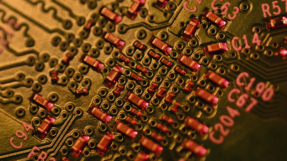
Embedded Components
Now, you can put resistors and capacitors inside PCB layers. This saves space and makes boards smaller and lighter. High-density interconnect PCBs give you more wires in less space. You get better signal quality and less noise. Fast signals work better with these boards.
| Benefits of HDI PCBs | Challenges of HDI PCBs |
|---|---|
| Higher wiring density per unit area | Extra precision needed for tiny pad sizes |
| Smaller and lighter boards | Possible crosstalk or noise from dense traces |
| Less stray capacitance and inductance | Picking the right material for laser drilling matters |
| Works with low-pitch IC packages | Risk of poor hole shape and quality |
| Reliable and supports fast signals |
There are some problems too. You need special tools and materials. You must watch for signal loss or heat problems.
System-in-Package (SiP) Trends
System-in-package technology lets you put many chips in one small package. This helps you make devices much smaller, even up to 65% smaller. You save money by making more at once and using simple designs. SiP makes products more reliable and easier to build. You can add antennas inside for better wireless signals.
| Trend | Description |
|---|---|
| Miniaturization | SiP lets you shrink system size by up to 65%. |
| Cost Reduction | You save money with bigger batches and easier assembly. |
| Simplification | SiP makes design faster and easier. |
| Yield and Manufacturability | You get better results and fewer mistakes. |
| Reliability | SiP gives you strong, long-lasting devices. |
| Antenna Integration | You can build antennas right into the package for better wireless signals. |
These new ways help you make smarter, smaller, and stronger devices.
Environmental and Regulatory Shifts
Eco-Friendly Materials
More companies now use eco-friendly materials for PCB manufacturing. These materials help keep the earth clean and people healthy. There are many new choices you can use:
- Lead-free options, like tin-silver-copper alloys, take the place of lead solder.
- Bio-based laminates use things like cellulose instead of oil.
- Halogen-free flame retardants are less toxic and make recycling simpler.
- Lead-free solders help keep workers and users safe from toxins.
- Halogen-free laminates make products safer and easier to recycle.
- RoHS-compliant parts help you follow tough environmental laws.
When you use these materials, you help stop pollution and make things safer for everyone.
Compliance and Lifecycle Management
You have to follow new rules for PCB design. These rules make sure products are safe and work well. You can use early computer tests to check for signal and heat problems. This lets you find issues before you build anything. You also test how strong your boards are with virtual stress checks.
You can do a better job with compliance by:
- Talking about risk so people know why safety is important.
- Using Compliance-by-Design, which means you add safety at every step and finish products faster.
- Making leaders more responsible for following the rules.
Good compliance keeps your products selling and keeps your company’s name safe.
E-Waste Reduction Strategies
You help cut down on e-waste by using smart ideas. These ideas help you save resources and make less trash:
- Design boards so they are easy to take apart and recycle.
- Pick green materials, like bio-based or halogen-free boards, to help the planet.
- Only make what you need, so you do not waste extra parts.
- Use closed-loop systems to recycle old boards and get back metals.
- Take care of your products from start to finish with extended producer responsibility.
These actions help protect the earth and help you follow new green rules.
Future Outlook for PCB Design & Layout
Anticipated Challenges
You will have some problems in pcb design & layout soon. Supply chain issues and not enough materials can slow your work. It is harder to get copper and resin now. This makes things cost more and causes delays. Shipping is also a problem, especially when you need parts from other countries. Finding skilled workers is not easy. Training people and keeping good workers is hard. You need a good place to work to get the best people. You also have to use green ways to follow new rules and help the earth.
- Supply chain disruptions
- Material shortages
- Need for skilled labor
- Adoption of sustainable practices
Note: Not having enough skilled workers can hurt your product quality. You should train and help your team learn new technology.
Opportunities for Innovation
You have many ways to make pcb design & layout better. AI algorithms can help you control signals and stop crosstalk right away. This makes your circuits work better and have fewer problems. You can use new materials like flexible and multi-layer PCBs. These make your devices smaller, stronger, and last longer. The market for pcb design & layout software is growing fast. More tools use AI to help you design better boards. You will see new features that make your work easier and faster.
- AI algorithms for real-time signal control
- Flexible and multi-layer PCBs for better performance
- Rapid growth in design software with AI optimization
Preparing for Industry Evolution
You need to get ready for big changes in pcb design & layout. Start using new technology like 3D structures and AI for faster devices. Use good design steps, like routing high-speed traces straight and using more layers for signals. Place ground and power planes in smart spots. Use solid power planes and put decoupling capacitors close to parts to keep power steady. For heat, pick low-power parts, use thermal vias, and add heat sinks or fans if needed. Try new ideas like embedded devices and ultra HDI designs to stay ahead. Using AI will help you fix design problems and make better products.
Tip: Keep learning and try new tools and ways to work. This will help you do well as the industry changes.
You see many new changes in PCB design and layout. AI tools, high-performance laminates, and 3D printing help you build better boards. To stay ahead, you should keep learning and plan for new skills.
- Learn new EDA tools and best practices.
- Work with suppliers and use parts from many vendors.
- Use automation and remote monitoring to improve your work.
- Watch for new trends and update your plans often.
By staying informed and flexible, you can lead in this fast-changing field.
FAQ
What is the main benefit of using AI in PCB design?
You get faster designs and fewer mistakes. AI tools suggest better layouts and catch errors early. This helps you save time and improve your board quality.
How do advanced materials help high-speed PCBs?
You use advanced materials to keep signals clear and fast. These materials reduce signal loss and heat. Your boards work better in 5G, AI, and IoT devices.
Why should you consider rigid-flex PCBs for wearables?
Rigid-flex PCBs let you build smaller, lighter, and more flexible devices. You can fit them into smartwatches or fitness bands. They bend without breaking and last longer.
How can you make your PCB designs more eco-friendly?
Choose lead-free solder and halogen-free laminates.
Design boards for easy recycling.
Use only what you need to reduce waste.
These steps help you protect the environment.