Design Guidelines for Reliable Rigid-Flex PCBs
When designing a rigid flex PCB, I always prioritize reliability and performance. Adhering to design guidelines ensures that the PCB withstands mechanical stress and maintains signal integrity. Flexible rigid PCBs often face challenges like delamination, signal loss, and manufacturing defects. Proper design minimizes these risks. Material selection, stack-up configuration, and bend radius play crucial roles in enhancing durability. I’ve seen firsthand how well-planned designs reduce failures and improve manufacturability. Following established guidelines is not optional; it’s essential for creating dependable rigid-flex PCB solutions.
Key Takeaways
- Choose the right materials for rigid-flex PCBs. Use FR-4 for stiff parts and polyimide for bendable parts to make them strong and flexible.
- Measure the bend radius carefully. For parts that don’t move, make it ten times the flex thickness. For moving parts, make it twenty times to avoid damage.
- Follow design rules to stay safe. Use standards like IPC-6013 to make sure your PCB works well and lasts long.
- Plan how you connect parts wisely. Keep trace widths the same and avoid sharp turns to keep signals clear and stop interference.
- Test the PCB carefully during production. Use heat tests and bending tests to check if it can handle tough conditions and lots of bending.
Overview of Rigid-Flex PCBs
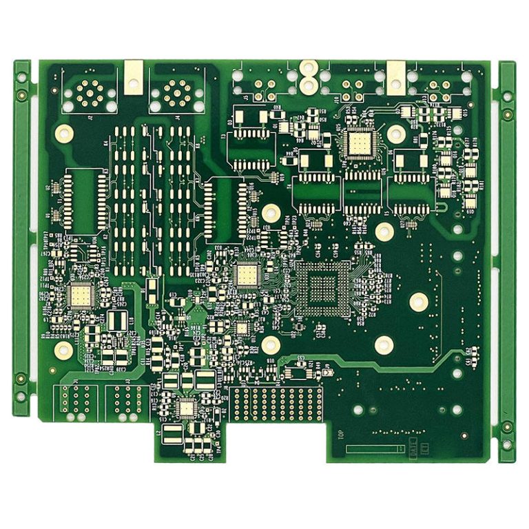
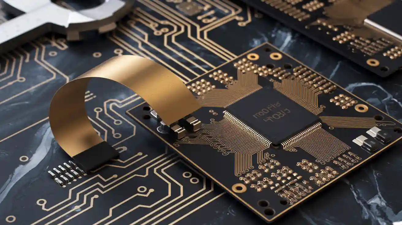
Structure and Composition of Rigid-Flex PCBs
When designing rigid-flex PCBs, I always start by understanding their unique structure. These PCBs combine rigid and flexible substrates to create a hybrid design that supports complex configurations. The rigid sections provide durability and mechanical support, while the flexible parts allow bending and movement.
| Structural Component | Description | Material Composition |
|---|---|---|
| Rigid Substrate | Provides durability and support for the PCB. | Commonly FR-4 or similar materials. |
| Flexible Substrate | Allows for bending and flexibility in design. | Typically polyimide or similar. |
| Hybrid Design | Combines both rigid and flexible elements for complex configurations. | Integration of rigid and flexible materials. |
I often use polyimide for flexible substrates due to its excellent thermal resistance and flexibility. For high-performance applications, DuPont™ Kapton® is a reliable choice, especially in aerospace and automotive designs. This combination of materials ensures the PCB can handle both mechanical stress and environmental challenges.
Advantages of Rigid-Flex PCB Designs
Rigid-flex PCBs offer several advantages that make them indispensable in modern electronics. Their ability to integrate rigid and flexible sections reduces the need for connectors and cables, which simplifies assembly and improves reliability. I’ve seen how this design minimizes signal loss and enhances electrical performance.
Some key benefits include:
- Space Efficiency: The compact design saves valuable space in devices.
- Durability: The hybrid structure withstands mechanical stress better than traditional PCBs.
- Improved Signal Integrity: Reduced interconnects lead to fewer signal disruptions.
- Cost Savings: Fewer components mean lower assembly costs.
These advantages make rigid-flex PCBs ideal for applications requiring high reliability and compact designs.
Common Applications of Rigid-Flex PCBs
Rigid-flex PCBs have become a cornerstone in industries that demand advanced electronic solutions. I’ve worked on projects where these PCBs were used in automotive systems, medical devices, and consumer electronics. Their versatility allows them to meet the needs of diverse applications.
| Application Area | Market Share (%) | Growth Driver |
|---|---|---|
| Automotive | 28.7 | Rise in electronic systems for vehicles |
| Multi-layer flex | 30.7 | Demand for high-density, high-performance PCBs |
| Asia-Pacific (China) | CAGR 12.4 | Increasing demand in consumer electronics and automotive |
In the automotive sector, rigid-flex PCBs support advanced electronic systems like ADAS (Advanced Driver Assistance Systems). In healthcare, they enable smaller, portable devices such as wearables and IoT-based medical equipment. The growing demand for high-density PCBs in consumer electronics further drives their adoption.
The North American PCB market highlights this trend. While rigid PCB production saw a slight decline of -0.9% in 2014, flexible circuit production dropped by -8.1%. Despite this, flexible circuits accounted for 11.8% of total PCB production value, reflecting their importance in specialized applications like aerospace and medical devices.
Design Guidelines for Rigid-Flex PCBs
Material Selection and Properties
When designing rigid-flex PCBs, I always prioritize material selection. The choice of materials directly impacts the PCB’s performance, durability, and flexibility. For rigid sections, I often use FR-4 due to its excellent mechanical strength and thermal stability. For flexible circuit boards, polyimide stands out as the ideal choice. Its high-temperature resistance and flexibility make it suitable for applications requiring repeated bending or exposure to harsh environments.
Copper type also plays a critical role. For static flex applications, I recommend using standard rolled annealed (RA) copper. It provides reliable conductivity and supports conservative bend radii, typically ten times the flex thickness. For dynamic flex designs, where repeated motion is expected, RA copper is still the best option, but I increase the bend radius to twenty times the flex thickness. This approach minimizes stress and extends the lifespan of the flexible sections.
Tip: Always match material properties to the application’s requirements. For high-stress areas, reinforce the rigid-to-flex interfaces and taper transitions to avoid stress concentration.
Stack-Up Design Considerations
The stack-up design is the backbone of any rigid-flex PCB. I carefully plan the layer configuration to balance electrical performance, mechanical stability, and manufacturability. A typical stack-up includes alternating layers of rigid and flexible materials, with copper traces sandwiched between dielectric layers.
Standardizing the stack-up simplifies manufacturing and ensures consistent quality. I specify tooling tolerances and layer thicknesses to avoid production errors. For high-density designs, I use thinner dielectric layers to reduce the overall thickness while maintaining signal integrity.
| Stack-Up Aspect | Recommendation |
|---|---|
| Layer Configuration | Alternate rigid and flexible layers for balanced performance. |
| Dielectric Thickness | Use thinner layers for high-density designs. |
| Tooling Tolerances | Specify precise tolerances to ensure manufacturability. |
Proper stack-up design also minimizes electromagnetic interference (EMI). By placing ground planes close to signal layers, I reduce noise and improve signal quality. This is especially important for applications like automotive systems and medical devices, where reliability is critical.
Bend Radius and Flexibility Requirements
Flexibility is the defining feature of rigid-flex PCBs, but it requires careful planning to avoid mechanical failures. I always calculate the bend radius based on the flex thickness and application type. For static flex designs, I use a conservative bend radius of at least ten times the flex thickness. This ensures the PCB can handle occasional bending without damage.
Dynamic flex designs demand greater flexibility. For these applications, I increase the bend radius to twenty times the flex thickness. This accommodates repeated motion and reduces the risk of copper fatigue.
Note: Never exceed the recommended bend radius. Sharp bends can cause delamination, cracking, and signal loss.
To further enhance flexibility, I avoid placing vias or components in high-stress areas. Routing traces perpendicular to the bend axis reduces stress and improves reliability. These design considerations ensure the PCB performs well under mechanical stress while maintaining signal integrity.
Routing Practices for Signal Integrity
Routing plays a critical role in maintaining signal integrity in rigid-flex PCB designs. I always approach this step with precision, as poor routing can lead to signal degradation, crosstalk, and electromagnetic interference (EMI). To ensure optimal performance, I follow a set of best practices tailored to the unique structure of rigid-flex PCBs.
First, I prioritize controlled impedance routing for high-speed signals. This involves maintaining consistent trace widths and spacing, as well as ensuring proper alignment with reference planes. For example, I use ground planes adjacent to signal layers to minimize EMI and maintain signal quality. This approach is particularly important in applications like automotive systems, where reliability is paramount.
Next, I avoid sharp corners in trace routing. Instead, I use smooth curves or 45-degree angles to reduce signal reflections and impedance mismatches. This simple adjustment significantly improves signal integrity, especially in high-frequency designs.
Tip: Always route traces perpendicular to the bend axis in flexible sections. This reduces mechanical stress on the copper traces and prevents cracking or delamination during bending.
Another key practice involves separating high-speed and low-speed signals. I ensure adequate spacing between these traces to prevent crosstalk. For differential pairs, I maintain consistent spacing and length matching to preserve signal integrity.
Finally, I avoid placing vias in flexible sections whenever possible. Vias can weaken the mechanical structure and introduce signal loss. If vias are unavoidable, I reinforce the area with additional dielectric material to enhance durability.
By adhering to these routing practices, I ensure that the rigid-flex PCB performs reliably under both electrical and mechanical stress.
Manufacturability and DFM Guidelines
Design for manufacturability (DFM) is a cornerstone of successful rigid-flex PCB production. I always incorporate DFM principles early in the design process to streamline the manufacturing process and reduce the risk of errors.
One of the first steps I take is to ensure compliance with industry standards, such as IPC-6013 and IPC-2223. These standards provide clear guidelines for rigid-flex PCB design, covering aspects like material selection, layer stack-up, and routing. I also review output files for compliance with specific customer requirements, such as Lockheed Martin’s stringent guidelines.
| Key Activities | Description |
|---|---|
| Compliance Check | Reviews output files for compliance with IPC standards and Lockheed Martin guidelines. |
| Design Error Identification | Identifies design errors and recommends revisions to improve manufacturability. |
| DFM Reporting | Findings are documented in a DFM report to ensure resolution before fabrication. |
During the layout process, I conduct thorough DFM checks to identify potential design errors. For example, I verify that the bend radius meets the specified requirements and that there are no vias or components in high-stress areas. These checks help prevent issues like delamination and mechanical failures during the manufacturing process.
Note: Standardizing the stack-up and specifying precise tooling tolerances can significantly improve manufacturability. This reduces production errors and ensures consistent quality across batches.
I also tailor the rigid-flex PCB layout to the specific requirements of the application. For instance, in high-density designs, I use thinner dielectric layers to reduce overall thickness while maintaining signal integrity. This approach is particularly useful in compact devices like medical wearables and consumer electronics.
By integrating these DFM practices, I ensure that the rigid-flex PCB design is not only functional but also manufacturable. This proactive approach minimizes production delays and enhances the overall reliability of the final product.
Manufacturing Considerations for Rigid-Flex PCBs
Key Manufacturing Processes
The manufacturing process for rigid-flex PCBs requires precision and expertise. I always emphasize the importance of sequential lamination, which ensures proper bonding between rigid and flexible layers. This step involves layering materials like FR-4 and polyimide, followed by controlled heat and pressure to achieve a seamless structure. Maintaining dimensional accuracy during lamination is critical to avoid misalignment.
Drilling and plating are equally vital. I use laser drilling for microvias in high-density designs, as it provides the precision needed for smaller features. Plating processes, such as electroless copper deposition, ensure robust electrical connections between layers. For flexible sections, I apply coverlays instead of solder masks to protect the circuitry while maintaining flexibility.
Testing is the final and most crucial step. I rely on automated optical inspection (AOI) and electrical testing to verify the integrity of the circuit board. These tests identify defects like open circuits or misaligned traces, ensuring the PCB meets quality standards before deployment.
Challenges in Rigid-Flex PCB Production
Producing rigid-flex PCBs comes with unique challenges. The transition between rigid and flexible sections often complicates the manufacturing process. I’ve encountered issues where improper bonding led to delamination, especially in high-stress applications. Sequential lamination demands precise dimensional control, which can be difficult to achieve without advanced equipment.
Cost is another significant factor. Rigid-flex PCBs are 4-8 times more expensive to produce than traditional rigid designs. This is due to the complexity of materials and processes involved. Additionally, achieving consistent quality across batches requires meticulous attention to detail, which increases production time and costs.
To address these challenges, I always collaborate closely with manufacturers. By sharing detailed design files and adhering to industry standards, I minimize errors and streamline production.
Ensuring Quality and Reliability During Manufacturing
Ensuring quality and reliability starts with robust design practices. I always verify that the stack-up and material selection align with the application’s requirements. During production, I work with manufacturers who follow IPC-6013 standards, as these guidelines ensure consistency and reliability.
Process control is another key factor. I monitor critical steps like lamination, drilling, and plating to ensure they meet specifications. For example, I specify tighter tolerances for high-density designs to prevent alignment issues. Regular inspections during production help catch defects early, reducing the risk of failures in the final product.
Post-production testing is non-negotiable. I use thermal cycling tests to evaluate the PCB’s durability under extreme conditions. Flexural testing ensures the flexible sections can withstand repeated bending without damage. These tests provide confidence that the rigid-flex PCB will perform reliably in its intended application.
Common Challenges and Solutions in Rigid-Flex PCB Design
Managing Stress Concentration in Flexible Sections
Stress concentration in flexible sections is one of the most common challenges I encounter when designing rigid-flex PCBs. The transition between rigid and flexible areas often creates weak points that are prone to mechanical failure. Without proper design considerations, these sections can experience cracking, delamination, or copper fatigue.
To address this, I always ensure smooth transitions between rigid and flexible sections. Abrupt changes in thickness or material properties can amplify stress. I taper the rigid-to-flex interface to distribute mechanical loads evenly. Additionally, I avoid placing vias, pads, or components near these transition zones, as they can act as stress concentrators.
Tip: Use teardrop-shaped pads at the ends of traces in flexible circuit boards. This reduces the risk of trace cracking during bending.
Another critical factor is the bend radius. I calculate the minimum bend radius based on the thickness of the flexible section. For static applications, I use a bend radius of at least ten times the flex thickness. For dynamic applications, where repeated bending occurs, I increase this to twenty times the thickness. This approach minimizes stress and extends the lifespan of the PCB.
Finally, I reinforce high-stress areas with stiffeners or additional dielectric layers. These reinforcements provide extra mechanical support without compromising flexibility. By implementing these strategies, I ensure that the flexible sections of the PCB can withstand mechanical stress without failure.
Addressing EMI and Signal Loss
Electromagnetic interference (EMI) and signal loss are critical challenges in rigid-flex PCB designs, especially in high-speed or high-frequency applications. Poor routing or inadequate shielding can lead to crosstalk, noise, and degraded signal integrity.
To mitigate EMI, I prioritize proper grounding and shielding. I place ground planes adjacent to signal layers to create a controlled impedance environment. This reduces noise and ensures consistent signal quality. For sensitive signals, I use copper shielding or EMI suppression materials in the stack-up.
Routing practices also play a significant role. I maintain consistent trace widths and spacing to avoid impedance mismatches. For differential pairs, I ensure equal trace lengths and spacing to preserve signal integrity. Additionally, I separate high-speed and low-speed signals to prevent crosstalk.
Note: Avoid routing traces parallel to the bend axis in flexible sections. This reduces the risk of signal degradation due to mechanical stress.
Signal loss can also occur due to poor material selection. I choose materials with low dielectric loss and high thermal stability to maintain signal integrity. For example, polyimide is an excellent choice for flexible sections due to its superior electrical properties. By combining these strategies, I ensure that the PCB performs reliably in demanding applications.
Preventing Delamination and Mechanical Failures
Delamination and mechanical failures are significant risks in rigid-flex PCB manufacturing and operation. These issues often arise from improper bonding, thermal stress, or poor material compatibility.
To prevent delamination, I focus on material selection and lamination processes. I use adhesives and prepregs that are compatible with both rigid and flexible materials. During lamination, I ensure that the temperature and pressure settings are optimized for the chosen materials. This creates a strong bond between layers and reduces the risk of separation.
Thermal stress is another common cause of delamination. I design the PCB to accommodate thermal expansion and contraction. For example, I use materials with similar coefficients of thermal expansion (CTE) to minimize stress at the rigid-to-flex interface.
Mechanical failures often occur due to sharp bends or excessive force on the PCB. I always adhere to the recommended bend radius and avoid sharp corners in the design. Additionally, I conduct flexural testing during the prototyping phase to evaluate the PCB’s durability under mechanical stress.
Callout: Regular quality checks during manufacturing can catch potential issues early. Automated optical inspection (AOI) and X-ray analysis are invaluable tools for ensuring layer alignment and bond integrity.
By addressing these challenges proactively, I ensure that the rigid-flex PCB remains reliable and durable throughout its lifecycle.
Designing a reliable rigid flex pcb requires strict adherence to established guidelines. I always emphasize the importance of selecting the right materials, planning an optimized stack-up, and calculating appropriate bend radii. Routing practices and manufacturability considerations also play a critical role in ensuring performance and durability.
By following these principles, designers can minimize risks like mechanical failures and signal loss. I recommend consulting industry standards such as IPC-6013 and IPC-2223 to ensure compliance and quality. Prioritizing reliability in every design decision leads to robust solutions that excel in demanding applications.
FAQ
What are the key materials used in rigid-flex PCB design?
I typically use FR-4 for rigid sections and polyimide for flexible areas. FR-4 provides mechanical stability, while polyimide ensures flexibility and thermal resistance. For copper layers, rolled annealed copper is ideal due to its durability and ability to handle bending stress.
How do I calculate the bend radius for flexible sections?
I calculate the bend radius by multiplying the flex thickness by a factor. For static applications, I use ten times the thickness. For dynamic designs, I increase this to twenty times. This prevents mechanical stress and extends the PCB’s lifespan.
Can rigid-flex PCBs handle high-speed signals?
Yes, but proper routing is essential. I use controlled impedance routing, maintain consistent trace widths, and place ground planes near signal layers. These practices reduce EMI and ensure signal integrity, even in high-frequency applications.
What testing methods ensure rigid-flex PCB reliability?
I rely on thermal cycling and flexural testing. Thermal cycling evaluates durability under temperature extremes. Flexural testing checks the flexible sections for repeated bending. Automated optical inspection (AOI) identifies defects like misaligned traces or open circuits.
How do I prevent delamination during manufacturing?
I select compatible materials and optimize lamination settings. Adhesives and prepregs must bond rigid and flexible layers effectively. I also ensure the materials have similar coefficients of thermal expansion to minimize stress at the rigid-to-flex interface.