You use multilayer pcb technology in many electronics every day. KING FIELD has more than 20 years of experience making multi-layer pcbs. They use the best machines and check quality carefully. The company follows IPC 610-D rules for materials and steps, so you always get good quality. You can look at what KING FIELD can do in the table below:
| Item | Capability |
|---|---|
| Layer Count | 1-40 layers |
| Board Thickness | 0.2-5.0mm |
| Min laser drill size | 4mil |
| Copper Thickness | 1/2 OZ to 10 OZ |
| Surface Treatments | ENIG, HASL, OSP, more |
You can change your multi-layer circuit board to work for any job. KING FIELD delivers fast, so your projects stay on time. Their smart way of making pcbs means you always get the best quality.
Key Takeaways
- Multilayer PCBs are very important in today’s electronics. They help make small designs with many circuits. Picking the right materials, like FR-4 or polyimide, affects how well your PCB works and how long it lasts. Careful drilling and plating make sure connections work well and stop problems in your PCB. Checking quality and testing at each step keeps standards high and lowers mistakes. KING FIELD delivers fast, with simple boards ready in 24 hours, so you can finish projects on time.
Material Selection for Multilayer PCBs
Choosing Substrates and Prepreg
When making a multi-layer pcb, you first pick materials. The substrate is the base of your board. What you choose changes how your pcb works and how long it lasts. KING FIELD gives you lots of choices for substrates and prepreg. You can see some common ones in the table below:
| Substrate Material | Key Characteristics | Common Applications |
|---|---|---|
| FR-4 | Cost-effective, good electrical insulation, mechanical strength, thermal stability | General applications |
| Polyimide | Superior thermal stability, flexibility | High-temperature, flexible-rigid applications |
| PTFE-based | Excellent high-frequency performance | RF and microwave applications |
| Ceramic | Exceptional thermal conductivity | High-power applications |
FR-4 is the most used material for printed circuit boards. It is cheap, strong, and works well with electricity. If you need something special, you might use polyimide or PTFE. These help your multi-layer pcb work in tough or fast jobs.
Prepreg is also important in making multi-layer pcbs. It sticks the layers together and changes how signals move. Here are some ways prepreg affects your pcb:
- Prepreg thickness and dielectric constant change signal quality in multi-layer designs.
- If prepreg is not even, signals can bounce back and cause trouble, especially in fast circuits.
- You can use more than one prepreg layer to get the right thickness and save money.
Good substrates and prepreg make your board last longer. Boards with better materials keep signals clear, even in rough places. For example, a board with a water-proof base can last years in wet spots, but a normal board may break sooner. Strong materials also help your pcb handle shaking or bumps.
Customization Options and Layer Count
You can change your multi-layer pcb to fit your needs. KING FIELD lets you pick how many layers you want, from easy to hard jobs. How you stack signal, power, and ground layers changes how your pcb works. More layers let you add more circuits and parts, but making them is harder. When you add layers, it takes more skill and time.
You pick the number of layers based on what your device needs. Devices that are small or fast often need more layers. KING FIELD can make up to 40 layers, so you can build advanced multi-layer pcb assembly for any job. Picking the right materials and smart design help you get the best results at every step.
Inner Layer Imaging and Etching
Multi-Layer PCB Patterning
The first step is making patterns on the inside layers. This is important because it controls how signals move in your multi-layer circuit board. Special imaging tools make these patterns clear and sharp.
- Laser Direct Imaging (LDI) gives you very detailed designs for your pcb.
- LDI can make trace patterns as tiny as 0.02mm.
- Photoimaging and etching help form copper traces on each inner layer.
Engineers must pick the right line width and space between lines. This helps your multi-layer pcb work well, even in hard jobs. LDI also helps stick layers together evenly during vacuum lamination. Using these tools makes your multi-layer pcb assembly strong and dependable.
Precision Etching for Circuit Accuracy
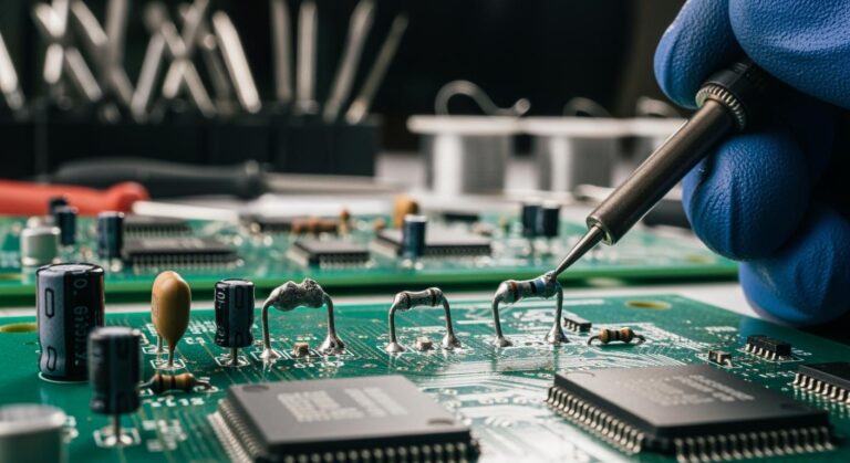
After imaging, you start etching. Etching takes away extra copper from the inner layers. Only the copper you need for your circuit stays. This is a key part of making a multi-layer pcb.
You have to watch the etching process closely. If too much or too little copper is removed, your pcb will not work right. KING FIELD uses smart machines to keep every trace just right. You get the same good results every time, even for boards with lots of parts.
Imaging and etching make sure lines and spaces are clean. This helps your multi-layer pcb handle fast signals and high power. Your multi-layer pcb will last longer and work better. By following these steps, you make sure your manufacturing is always top quality and very precise.
Tip: Always check your inner layers before you move on. Checking early saves time and stops mistakes in your multi-layer pcb.
Layer Alignment and Lamination Process

Multi-Layer Registration Techniques
Every layer in a multilayer pcb must line up just right. If layers are not lined up, the pcb will not work well. Special machines help keep each layer in the correct spot. KING FIELD uses smart systems to check and fix the position of each layer before pressing them together.
You can see how close the layers need to be in the table below:
| Design Type | Tolerance |
|---|---|
| Standard Multilayer | ±25 µm |
| Advanced HDI | ±7.5 µm or better |
These small tolerances stop short circuits and signal loss. If your pcb has many layers or is very detailed, you need even more accuracy. KING FIELD’s tools and checks make sure your multi-layer pcb always meets these rules.
Lamination for Defect Prevention
Lamination is an important step in making a multi-layer pcb. You press all the layers together using heat and pressure. This step holds the layers tight and makes the pcb strong. If you do not control this step, problems can happen that hurt your board.
Here are some common lamination problems and ways to stop them:
- Lamination voids can make your pcb weak and cause electrical trouble.
- Not enough resin flow or wrong settings can make voids.
- Uneven copper, wet spots, or bad stack-up can also cause issues.
- You can stop these problems by:
- Using good prepreg
- Testing resin flow before starting
- Balancing copper and spacing layers well
- Setting the right heat, pressure, and time
- Using vacuum lamination to get rid of air
- Pre-baking materials to keep out moisture
- Watching the process closely as you work
KING FIELD’s smart lamination and real-time checks help you avoid these problems. You get a strong and dependable pcb for any job. By following these steps, you make sure your multi-layer pcb stays accurate and tough during every part of making it.
Drilling, Via Formation, and Plating

High-Precision Drilling for Multi-Layer PCBs
Drilling is the first step in making a multi-layer pcb. This step makes holes called vias. Vias connect the layers inside your pcb. You need to be very careful when drilling. Each hole must be in the right place. If you miss, the pcb may not work well. You must watch out for several things:
- Hole position tolerance keeps holes where they should be.
- Hole diameter consistency makes sure every via fits right.
- Hole wall quality stops rough edges and helps electricity flow.
- Alignment with copper layers makes sure the pcb works.
You use special drilling machines to get good results. These machines must be very accurate. Not all machines can drill with tight tolerances. The material of the pcb changes how the drill works. If the pcb is thicker or thinner, the drill moves differently. Layers must line up perfectly. If not, the drill may go too deep or not deep enough. You plan your stackup and via strategy before you start. You pick back drill sizes 4–8 mil bigger than the original via. You keep enough annular rings on capture pads. You mark nets for back drill in notes and give layer target depths and drill files.
Tip: Always check your drilling accuracy before you move on. Checking now helps you avoid problems later in pcb testing.
Copper Plating and Via Reliability
After drilling, you add copper plating. This step covers the inside of each via with copper. You follow rules like IPC-6012 and IPC-2221. These rules say how thick the copper must be in vias. Thicker copper helps your pcb carry more current. You must size your vias so plating stays even.
Good copper plating makes your pcb strong. If the copper is not thick enough, weak spots can form. You control via aspect ratio and plating steps to keep conductivity and strength. Proper plating lowers the risk of electrical or mechanical failure. You make sure every connection in your pcb stays strong.
You use the pcb manufacturing process to build boards that work well. You check each step, from drilling to plating, to make sure everything is right. You get your pcb ready for lamination and the next step in making multi-layer pcbs.
Outer Layer Processing and Quality Control
Outer Layer Imaging and Solder Mask
You begin the last steps by making patterns on the outside layers. These patterns are copper lines and pads that connect your parts. It is important to keep these lines neat and correct. If you do not, your pcb can have problems like shorts or broken paths.
Here is a table that shows some common problems, what causes them, and how to fix them:
| Defect | Description | Causes | Solutions |
|---|---|---|---|
| Solder Bridging | Unwanted connection between paths that makes a short. | Too much solder paste, parts not lined up, bad printing, wrong heat. | Change stencil design, use AOI, add solder mask, check machines. |
| Open Circuits | A break in the path stops electricity from flowing. | Not enough etching, holes not lined up, layers coming apart, weak solder. | Check quality, use better materials, improve soldering. |
| Delamination | Layers come apart because they do not stick well. | Too much heat, water, bad lamination, weak materials. | Use water-proof materials, bake boards first, fix lamination. |
| Insufficient Copper | Copper is too thin, so it heats up more. | Not enough plating, wrong current, old plating baths. | Watch plating, use good plating, check with cross-section. |
| Misalignment of Layers | Layers inside do not line up right, causing problems. | Bad lamination, materials move, holes not even. | Use optical tools, add marks, keep pressure even. |
| Via Defects | Problems with vias can hurt signals. | Bad plating, air bubbles, drilling mistakes, heat stress. | Make plating better, use good drills, plan for heat. |
| Blistering and Bubbles | Raised spots on the pcb can cause trouble. | Water trapped, too much heat, bad lamination. | Bake materials, keep clean, fix lamination settings. |
| Solder Balling | Small balls of solder can make shorts or noise. | Too much flux, wrong solder paste, bad heating. | Change paste, control heat, clean boards well. |
You can stop many of these problems by using a solder mask. The solder mask covers the copper lines and keeps them safe from air. It also stops solder from making bridges between pads. This layer helps keep the board strong and makes it last longer, even in hard places.
You can pick different finishes for your pcb. Each finish has its own use and good points. Here is a table to help you compare them:
| Surface Finish | Description | Thickness | Shelf Life | Applications |
|---|---|---|---|---|
| HASL | Cheap and easy, uses melted solder. | 1–50 μm | 6–12 months | Everyday electronics, cars (not for important parts) |
| ENIG | Flat and tough, uses nickel and gold. | 3–6 μm (nickel), 0.05–0.1 μm (gold) | 12–18 months | Planes, medical, fast signals |
| OSP | Thin layer made from organic stuff. | N/A | Short time | Cheap, lead-free boards |
You choose the finish that fits your job. ENIG is flat and strong for important work. HASL is good for most uses. OSP is best for cheap, lead-free boards. Each finish keeps copper safe, helps with soldering, and changes how your pcb works over time.
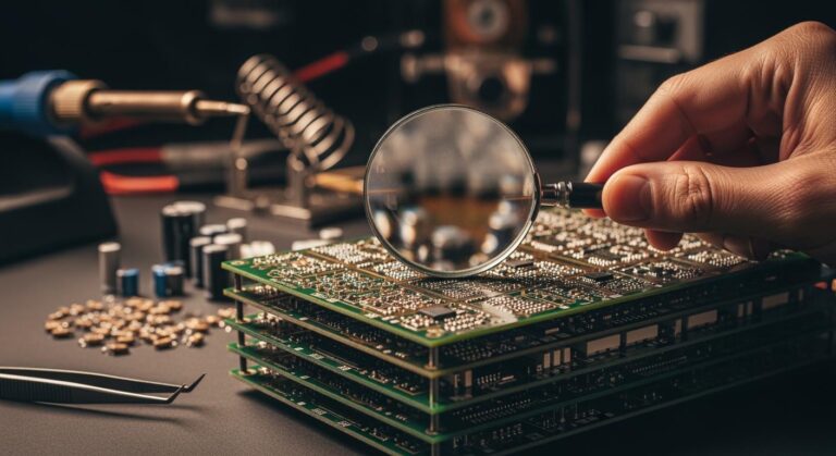
Electrical Testing and Final Inspection
You must test your pcb before sending it out. This is called multi-layer pcb testing. You use different tests to make sure all parts work and are safe. Here are the main tests:
- Electrical Tests (Continuity and Isolation): You check if points are connected and if others are kept apart.
- Functional Testing: You run the pcb to see if it works as it should.
- In-Circuit Testing (ICT): You test each part to find breaks or wrong values.
You also look for any problems you missed. You check for bad solder, missing parts, or scratches. Machines and trained people check every board.
KING FIELD checks quality at every step. Most boards pass the first test. For quick jobs, 95-98% pass right away. This shows the process works well and gives you good boards.
You also get your boards fast. KING FIELD can finish simple boards in 24 hours. Harder boards take up to three weeks. This speed helps you finish your projects on time.
You can pick the specs you need. KING FIELD offers small holes down to 0.075mm and copper from 1/2oz to 14oz. You can also get a solder mask plug hole up to 0.5mm. These choices give you the right fit for any job.
Note: Careful testing and checking at every step help you avoid problems and get the best results from your pcb.
You can see that every step in making multilayer PCBs is careful. KING FIELD checks their work often to catch mistakes early. They use in-circuit testing to make sure everything works right. They also follow ISO 9001 rules to keep quality high.
| Quality Control Practice | Impact on Failure Rates |
|---|---|
| Regular audits | Fewer defects |
| In-circuit testing | Reliable performance |
| ISO 9001 certification | Higher product quality |
KING FIELD has over 28 years of experience helping many industries. They work with AI, cars, and healthcare companies. They deliver 98.9% of orders on time. Customers give them great reviews because they care about doing a good job.
FAQ
What is a multilayer PCB?
A multilayer PCB has three or more layers of copper. You use it to connect many circuits in a small space. This design helps your device work faster and handle more features.
How many layers can KING FIELD make for my PCB?
You can order PCBs with up to 40 layers from KING FIELD. This lets you build advanced products for industries like medical, automotive, or industrial control.
How fast can I get my multilayer PCB from KING FIELD?
You can receive simple boards in as little as 24 hours. Complex boards may take up to three weeks. Fast delivery helps you keep your project on schedule.
What surface finishes can I choose for my PCB?
You can pick from ENIG, HASL, OSP, and more. Each finish protects copper and helps with soldering. The right finish depends on your device’s needs.