When you learn PCB layout, you control how well devices work. Using pcb design basics helps you manage heat and avoid problems when making the board. It also makes putting the board together easier. If you follow design rules like the right track width and spacing, your pcb will meet standards and last longer. KING FIELD has over 20 years of experience to help you see PCB layout as a challenge and a chance to be creative.
Key Takeaways
- Good PCB layout is very important for how devices work and last. You should follow design rules to stop common problems.
- Where you put components helps control heat and keeps signals clear. Place parts in smart spots to make the board work better.
- Use the right trace routing to keep signals strong. Make sure traces are wide enough and do not mix signals.
- Check your design often to find mistakes early. Work with experts to make sure your PCB follows all rules.
- Follow PCB design rules like spacing and grounding. These steps stop electrical issues and make building easier.
What Is PCB Layout
PCB Layout Definition
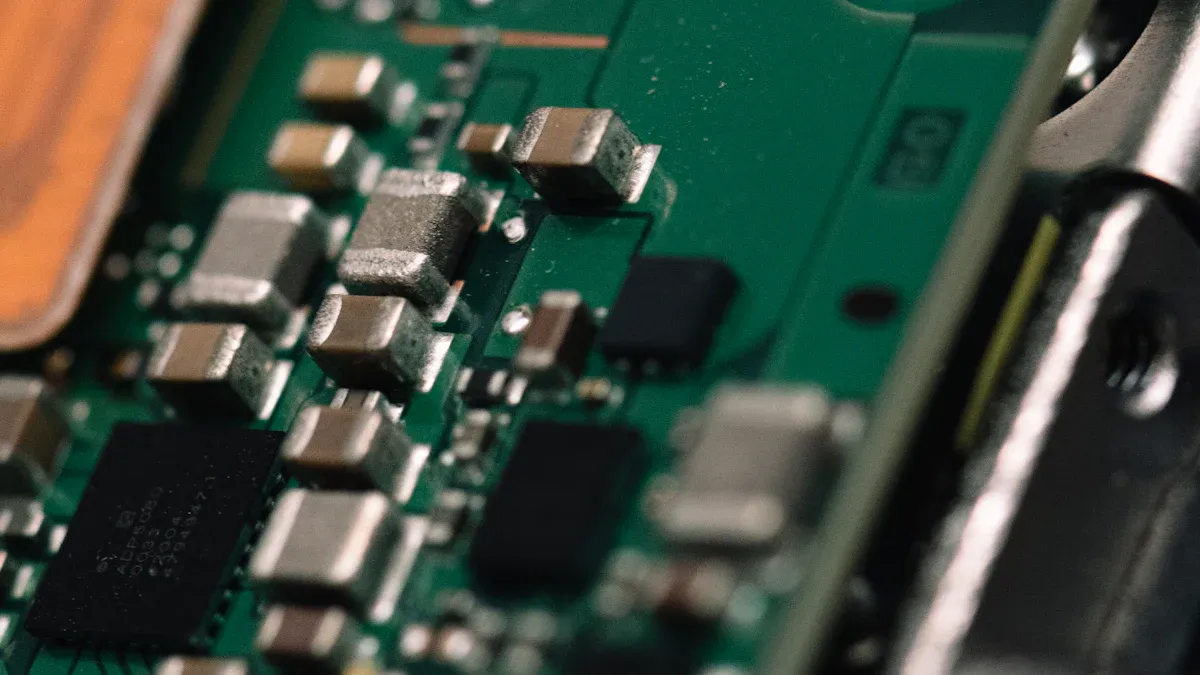
You might ask what pcb layout is when you start with electronics. PCB layout design means turning your idea into a real circuit board. You put parts in place and make connections so your device works. This step takes your schematic and makes it into a board you can build and use.
When you set up parts and connect them on a pcb, you make sure each part gets power and signals. You use pcb design basics to pick where parts go and how traces link them. Good layout helps stop problems like losing signals or getting too hot. You pick materials like FR-4 for most boards or PTFE for high-frequency ones. These choices change how your board handles heat and signals.
Tip: Always look over your schematic before you start your pcb layout. This helps you find mistakes early and saves time.
Why PCB Layout Matters
You need to know pcb layout because it changes how your device works and how long it lasts. Bad pcb layout can cause up to 70% of electronic failures. If you use controlled impedance traces, you can cut signal reflections by up to 90%. This makes your board work better, especially for fast signals.
A good layout gives you better results. Here are some ways pcb layout helps:
- You make the loop area smaller for high-frequency signals, which lowers inductance and helps performance.
- You use good grounding to stop voltage changes that can hurt your boards.
- You pick the right materials to keep signals clear and control heat.
When you follow pcb design basics, you make boards that meet standards and work well. You make smart choices to stop common problems. This is why learning pcb layout is important for anyone who wants to make reliable electronics.
PCB Layout Process with KING FIELD
You need a good plan to make strong circuit boards. KING FIELD uses steps to help you turn ideas into real products. You work with experts who help you at every stage. They make sure your pcb fits your needs and follows rules.
Requirements Analysis
First, you collect all the facts about your project. KING FIELD talks with you to learn what you want your pcb to do. You think about the size and shape of the board. You also look at how the board will be used. You decide how the board will be made and what materials you need. Here are some main things you look at:
- Knowing board limits
- How to make the board
- Materials and parts
- Order for placing parts
- How parts face
- How the layout is set up
You share your goals and any special needs you have. This helps KING FIELD make a plan that fits your project. You check the design to make sure it matches what you want before you move on.
Component Placement
You pick where each part goes on the pcb. This step is important for how well your board works. It also helps make building the board easier. KING FIELD uses smart tools to help you put parts in the best places. You think about heat, signal paths, and how parts connect.
Here is how good placement helps your pcb:
| Aspect | Impact on PCB Layout |
|---|---|
| Thermal Management | Good placement keeps the board cool and makes it last longer. |
| Crosstalk Minimization | Putting parts in the right spots keeps signals clear. |
| Solderability | Smart placement makes soldering easier and cuts down on mistakes. |
| Automated Assembly | Where you put parts helps machines build the board faster. |
| Soldering Processes | Good placement stops parts from moving and keeps them in place. |
| Performance | Smart placement makes the board work better and stay cool. |
| Subcircuit Identification | Finding small circuits helps use space well. |
| Signal Pathways | Short paths keep signals strong and clear. |
| High/Low Voltage Separation | Keeping high and low voltage parts apart keeps signals safe. |
You use these ideas to make your pcb work well and easy to build.
Trace Routing
You draw lines called traces to connect the parts. These lines carry signals and power. KING FIELD helps you draw traces so your pcb works right. You follow good rules to keep signals strong and stop problems.
Here are steps you follow for good trace routing:
- Know what signals you need. You check how fast and what kind of signals you have.
- Pick how many layers your pcb needs to keep signals strong.
- Make sure data lines are the same length for timing.
- Make traces the right width and use the right materials.
- Keep traces apart so signals do not mix.
- Use tools to check for problems before you build the board.
- Use ground planes to help signals return safely.
- Add parts to stop signals from bouncing back.
KING FIELD uses computer tools to check your design and fix problems before you build.
Design Review and Support
You check your design with KING FIELD before making the pcb. This step helps you find mistakes and fix them. You work with experts who know how to build boards. You use lists to check every part of your design. You also get advice from people who make the boards.
Here is how KING FIELD helps you during design review:
| Best Practice | Description |
|---|---|
| Design for Manufacturability (DFM) | Reviewers look for mistakes that could cause problems when making the board. |
| Diverse Reviewers | People not on the design team check for mistakes others miss. |
| Internal Manufacturing Team | Experts give tips to make your pcb easy to build. |
| Use of Checklists | You use a list to check every part of your design. |
| Functional Interfaces | You make sure all parts fit and work together. |
| Manufacturer’s Perspective | You check if your design has all the info needed to build it. |
| Address Feedback | You fix any problems found before you finish the design. |
You also get help from KING FIELD after the design is done. If you have questions or problems, you can ask for help. KING FIELD uses computer models to find problems early. You get help from both design and building teams. This makes your pcb layout process easy and helps you avoid mistakes.
Tip: Working with the building team helps you find problems early and save money. You get faster results and better boards.
You use KING FIELD’s layout service to make sure your pcb is strong, easy to build, and ready to use.
PCB Design Principles
You should use good pcb design principles. This helps your board work well and last longer. These rules guide you in every step of pcb layout. KING FIELD uses these rules to help you get strong results.
Component Clearance
You need space between parts on your pcb. This stops short circuits and makes fixing easier. IPC 2221 says you need 10 mils space for up to 50V. UL 60950 wants 15 mils for strong insulation up to 250V. If you use 100V on an outside layer with no coating, IPC 2221 says use 0.6mm space. You keep your board safe by following these rules. KING FIELD checks every design to make sure you follow them.
- Space parts for safety and easy building.
- Use the right space for your voltage.
- Check your board for tight spots before you finish.
Note: Enough space helps you stop electrical problems and makes your pcb easier to build.
Solder Mask and Pads
You need good solder mask and pad design to stop solder from joining where it should not. Solder Mask Defined (SMD) pads set the exact spot for solder. This helps with small, crowded parts. Non-Solder Mask Defined (NSMD) pads give stronger joints and better support. You must keep pads apart so solder does not flow between them. KING FIELD uses these rules to make your board easy to put together.
- Use NSMD pads with extra mask for most SMT parts.
- Do not use 1:1 mask-to-copper openings unless needed.
- Keep copper 4 to 6 mil away from the edge of a solder resist opening.
If you follow these rules, you lower the chance of solder joining and exposed copper. KING FIELD checks every pcb for good solder mask space.
Routing Width and Vias
You must pick the right trace width and via size for your pcb. Bigger vias cost less and need bigger pads. Bigger pads make your board stronger. IPC-2221 gives rules for pad and via size. IPC-2222 helps you pick the right hole size for crowded boards. KING FIELD uses these rules to make sure your board can handle the current and works well.
- Make pad size bigger than via size, especially for wide traces.
- Use bigger pads for more strength.
- Pick via type based on layer count, especially if you have more than 8 layers.
Tip: Following routing rules helps you stop problems with current and signal loss.
EMI and Thermal Management
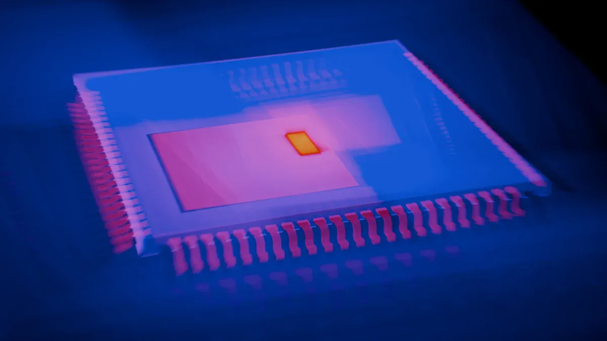
You must control EMI and heat to keep your pcb working right. Good pcb layout uses ground planes and smart trace paths to lower EMI. You can add filters like ferrite beads to block high-frequency noise. Put noisy parts away from sensitive ones. Use heat sinks and thermal vias to move heat away from hot spots. KING FIELD uses these rules in every design to keep your board safe.
- Use ground planes to lower EMI.
- Add filters to block noise.
- Place parts to keep noisy and sensitive areas apart.
- Use heat sinks and thermal vias for better cooling.
If you control EMI and heat, your pcb lasts longer and works better.
Manufacturability
You need to design your pcb so it is easy to make. Choices about layout, materials, and tolerances change how hard it is to build your board. If you use Design for Manufacturability (DFM) early, you find problems before making the board. KING FIELD checks every design to make sure you can build it without trouble.
- Check your design early to fix problems.
- Pick parts and materials that are easy to get.
- Use tolerances that match your manufacturer’s skills.
KING FIELD follows rules like IPC-2221 and UL certification. The team uses tests and checks to look at every pcb. You get a board that meets high standards and is ready to use.
| Certification/Standard | Description |
|---|---|
| UL | Underwriters Laboratories certification for safety standards |
| IPC Class 3 | High reliability standards for electronic assemblies |
| ISO 9001 | Quality management system standards |
| ISO 13485 | Quality management for medical devices |
| IATF 16949 | Quality management for automotive production |
| ISO 45001 | Occupational health and safety management |
| ISO 14001 | Environmental management standards |
| ISO 50001 | Energy management standards |
You can trust KING FIELD to use good pcb design rules in every project. The team checks your pcb for rules like IPC-2221, UL, and others. You get a board that is safe, strong, and easy to make.
Remember: Using these rules helps you avoid mistakes and makes your pcb layout strong.
Practical PCB Layout Tips
Common Mistakes to Avoid
You can stop many problems in pcb by learning from mistakes. Many new people make errors that cause boards to break or be hard to fix. The table below lists some mistakes and ways to stop them:
| Mistake | Description | How to Avoid |
|---|---|---|
| Incorrect Trace Width | Traces that are too thin can get hot and break. | Use trace width tools and keep power traces wide. |
| Poor Pad Spacing | Pads close together can cause solder to join or stand up. | Use standard footprints and give space for solder mask. |
| Ineffective Grounding Strategy | Floating grounds make noise and signals not stable. | Use a solid ground plane and connect layers with vias. |
| Poor Via Placement | Bad via spots hurt signal and heat flow. | Do not put vias on pads and use more thermal vias. |
| Overlooking Component Orientation | Parts not lined up right cause mistakes when building. | Line up polarized parts and ICs for easy building. |
You should also check fiducial marks, pick good materials, and follow best pcb layout steps to stop mistakes.
Tools and Resources
You have many tools to help with pcb. Some tools have smart features like rule checks, auto-routing, and 3D views. These features help you find problems early and fix them fast. Here are some popular software choices:
| Software Tool | Key Features | Cost Type |
|---|---|---|
| Altium Designer | 3D views, simple to use, team tools | Premium |
| Autodesk EAGLE | Big library, easy to use, works with other programs | Free/Paid |
| KiCad | Open-source, 3D views, large community | Free |
| Altium CircuitMaker | Free, like pro version | Free |
| LibrePCB | Simple, works on many computers, no account needed | Free |
| Fusion 360 | Combines pcb with CAD and CAM | Paid |
You can learn more from online guides like The Best Free Resources for Learning PCB Design in 2026 and Top 10 PCB Design Software Tools for Engineers in 2025.
Reviewing Your Design
You should always check your pcb before making it. Checking often helps you find mistakes early and makes boards work better. You can use lists to make sure you follow all rules. Reviews help you learn from old boards and update your steps. Here are some tips for a good review:
- Ask others for feedback, not just your team.
- Use lessons from real boards to make your next one better.
- Focus on what the board needs and how to build it.
- Use tools that find mistakes and help you follow rules.
When you check and update your design, you make better boards and save time. KING FIELD uses these steps to help you get strong results every time.
You can get good at PCB layout by working on signal integrity, putting parts in smart places, and drawing traces well. Put parts that work together close to each other. Use ground planes to help your board work better. Place parts so heat does not build up. If you use KING FIELD’s Layout Service, you get help from people who know a lot and check for quality.
| Benefit | How KING FIELD Helps |
|---|---|
| Expert Team | More than 10 years of design experience |
| Full Service | Help from idea to finished product |
| Quality Assurance | High standards for every project |
You get better at PCB layout and make stronger electronics when you keep learning and use these tips.
FAQ
What is the most important rule in PCB layout?
You must keep enough space between parts and traces. This helps prevent short circuits and makes your board safer. Always check the spacing rules for your project.
How do you choose the right PCB design software?
You should pick software that matches your skill level and project needs. Beginners often use KiCad or Autodesk EAGLE. Professionals may use Altium Designer or Cadence.
Why do you need a ground plane on your PCB?
A ground plane helps control noise and keeps signals stable. It also improves the performance of your board. You should use a solid ground plane for best results.
Can you fix PCB layout mistakes after manufacturing?
You cannot change the layout after making the board. You must review your design carefully before production. Always double-check your files and ask for expert help if needed.
