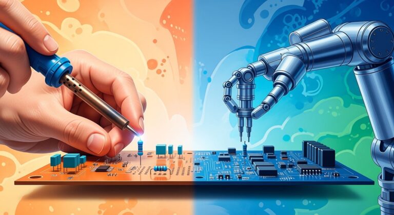
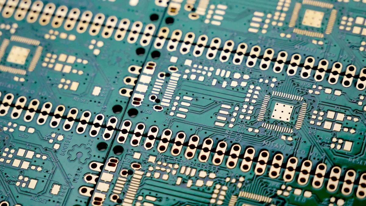
You begin circuit board assembly after the printed circuit board is made. Every step on the pcb assembly line is important. These steps help make electronics that work well. In mass production, you must follow exact steps to make strong printed circuit boards. The process has many stages. Here is what you see in a normal pcb line:
- Design for Assembly (DFA)
- Surface Mount Device (SMD) assembly
- Solder paste application and inspection
- Reflow soldering
- Board cleaning
- Through-hole component assembly
- Soldering non-washable components
- Circuit board testing
- Final inspection
If you know each pcb step, you can see how good products are made.
Key Takeaways
- Learn how the circuit board assembly works. Every step matters, from putting on solder paste to checking the board at the end. These steps help make electronics that work well.
- Use the right way to put on solder paste. Good printing makes strong solder joints. It also stops problems like solder bridges.
- Look closely at where you put each part. Make sure every piece faces the right way. This helps the circuit work as it should.
- Use quality checks often. Inspections like Automated Optical Inspection (AOI) find mistakes early. This keeps the work at a high level.
- Pack circuit boards safely for shipping. Use materials that keep out moisture and stop static. This protects the boards while they travel.
Solder Paste Application in PCB Assembly Line
Solder Paste Printing Process
You begin assembly after the pcb manufacturing process ends. The first thing you do is solder paste printing. This step gets the board ready for putting on parts. Most factories use a stencil to put on the solder paste. The stencil acts like a screen in screen-printing. It covers the pcb and lets paste go only where needed. You put the stencil on the board and spread the paste. The paste goes through the holes in the stencil. It lands on the pads of the pcb.
There are different ways to print solder paste. Here is a table that lists the most common ones:
| Method | Description | Advantages | Limitations |
|---|---|---|---|
| Direct Ink Writing | Advanced precision dispensing using a fine nozzle for controlled application. | High precision, minimal waste, good for complex PCBs | More expensive and complex than other methods |
| Screen Printing | Traditional method using a stencil to transfer solder paste. | High throughput, ideal for mass production | Less precision, needs high-precision stencils |
| Jet Dispensing | Uses a nozzle to jet droplets of solder paste without a stencil. | Flexible, good for small or odd areas | Higher cost, slower than other methods |
Screen printing is used the most for making many boards. Other ways work better for special boards or small batches.
Importance of Accurate Application
It is important to print solder paste carefully for a strong pcb. You must line up the stencil with the pcb using fiducial marks. If you do not line it up right, you can get problems like solder bridges. The stencil thickness matters too. For example, a 0.10 mm stencil is best for small parts. A 0.15 mm stencil is better for big pads.
You need clean and pure materials for this step. Dirty boards or paste can make weak solder joints. The table below explains why being clean is important:
| Aspect | Description |
|---|---|
| Clean Surfaces | Helps solder stick well and form strong joints |
| Contaminants | Dirt or oil can stop solder from sticking, causing weak joints |
| Recommended Solvents | Pure alcohol cleans surfaces for the best solder joint quality |
Tip: Always clean the pcb before you print solder paste. Use pure alcohol to get rid of oil and sweat.
You must watch each step in the process. Good solder paste printing makes boards work well and helps production go smoothly. If you follow these steps, you help make strong and high-quality electronics.
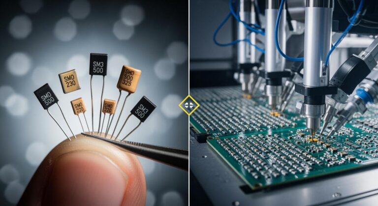
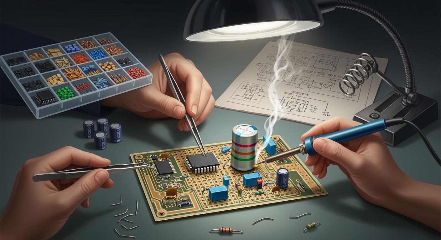
Component Placement on Printed Circuit Board
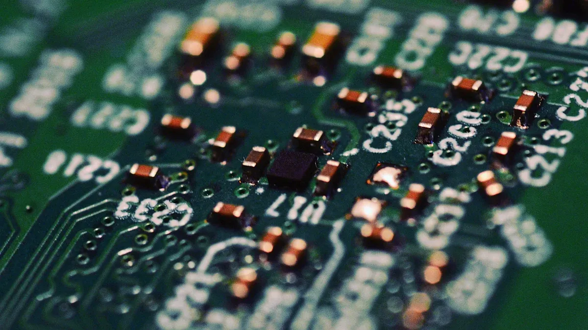
After you finish solder paste application, you start placing components. This step means putting each part on the pcb. You can use machines or do it by hand. You need to be careful so every part goes in the right spot.
Surface Mount Technology (SMT)
SMT is used for most mass production. Machines pick up tiny parts and put them on the pcb fast. These machines can place many parts quickly. For example, an SMT machine puts a two-pin part in 0.45 seconds. This speed helps you finish production faster.
| Component Type | Cycle Time (seconds) | Example Calculation |
|---|---|---|
| SMT (2 pins > 0402) | 0.45 | 37.35 seconds for 5 components on top and 78 on the bottom |
SMT works well because parts have standard sizes. This makes it easier to place them exactly right. You get more good boards and fewer broken parts. You must check the direction of each part. If you put a part the wrong way, signals can get messed up. This can make your printed circuit boards work badly.
Tip: Always check the direction of polarized parts like diodes and capacitors before you start.
Through-Hole Component Placement
Through-hole placement is for parts that need strong connections. You push the leads of each part through holes in the printed circuit board. You can do this by hand or with a machine. Hand placement is best for small batches or special boards. Machines help with big jobs, but they are slower than SMT machines. For example, a through-hole part with two pins takes about 60 seconds to place.
| Technology Type | Assembly Speed | Reliability | Notes |
|---|---|---|---|
| Surface Mount Technology (SMT) | Faster because of machines | Not as strong; failure rates around 0.5-1% in normal conditions | Needs good design for tough places |
| Through-Hole Technology (THT) | Slower | Stronger; failure rates below 1% in hard conditions | Best for places with lots of shaking or stress |
Through-hole placement gives more strength. You use it for connectors or parts that get bumped or moved. You must always check where and how you put each part. If you get it wrong, testing and soldering get harder. Your pcb will not be as reliable.
You need to place parts carefully for both SMT and through-hole. Good placement helps your process and keeps your printed circuit boards strong and working well.
Soldering Process in Circuit Board Assembly
After you finish component placement, you move to the soldering step. This part of the circuit board assembly process joins each component to the pcb. You use different soldering methods depending on the type of component and placement. The right soldering technique helps you avoid solder defects and keeps your printed circuit board strong.
Reflow Soldering for SMT
You use reflow soldering for most surface mount components. This method works well for mass production on the pcb assembly line. In reflow soldering, you heat the pcb in a special oven. The solder paste melts and connects each component to the board. You must follow a careful temperature profile to get good results.
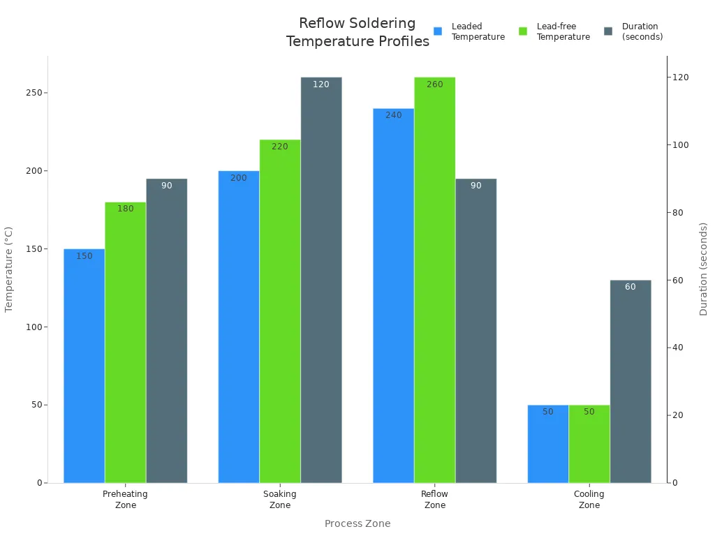
The reflow process has four main zones. Each zone has a different temperature and time. You can see the details in the table below:
| Zone | Temperature Range (°C) | Duration (seconds) | Key Notes |
|---|---|---|---|
| Preheating Zone | 25 to 150 (leaded), up to 180 (lead-free) | 60 to 90 | Ideal preheat rate: 1-3°C/s to avoid thermal shock. |
| Soaking Zone | 150 to 200 (leaded), 180 to 220 (lead-free) | 60 to 120 | Ensures flux activation and uniform temperature across the PCB. |
| Reflow Zone | 210 to 240 (leaded), 240 to 260 (lead-free) | 30 to 90 | Peak temperature should be 20-40°C above solder melting point. |
| Cooling Zone | Below 50 | 30 to 60 | Cooling rate: 2-4°C/s to prevent brittle joints. |
You can also look at this chart to see how the temperature changes during reflow soldering:
You have a few options for the reflow profile:
- Ramp-Soak-Spike (RSS) Profile: You control the temperature change step by step to prevent defects.
- Ramp-to-Spike (RTS) Profile: You increase the temperature steadily. This works well for lead-free soldering.
- Custom Profiles: You can adjust the profile for special boards or unique solder paste.
You must watch the temperature closely. If you heat the pcb too fast, you can damage components. If you heat it too slow, you may not get good solder joints. Good reflow soldering helps you avoid common problems like tombstoning, where a component lifts off the board, or cold joints, where the solder does not melt enough.
Wave and Hand Soldering for Through-Hole
For through-hole components, you use wave soldering or hand soldering. Wave soldering is common for large batches on the pcb assembly line. You move the pcb over a wave of hot solder. The solder flows around the leads and makes strong connections. You must set the right angle, wave height, and temperature for the best results.
Here are some best practices for wave soldering:
| Best Practice | Description |
|---|---|
| Process Optimization | Adjust conveyor angle, wave height, and temperature for complete joint coverage. |
| Precautions | Use solder mask to prevent unwanted solder adhesion and thermal relief pads to protect sensitive components. |
| Design Considerations | Provide thermal relief for plated through holes connected to large copper planes to ensure proper solder flow. |
| Process Considerations | Ensure adequate flux penetration and avoid excessive heat to improve solder fill. |
You can use tools like the Fluxometer and Waverider to check the process and make sure everything is even. If you have large copper planes, you should add thermal relief. This helps the solder flow better and gives you strong joints.
Hand soldering is important for small batches or special boards. You use a soldering iron to join each component by hand. You must hold the iron at a 45-degree angle for the best heat transfer. Use just enough solder to cover the joint. Do not use too much or too little.
Here are some common issues you may see during manual soldering and how to fix them:
- Cold Joints: Not enough heat. Make sure the iron is hot and touches both the lead and pad.
- Solder Bridges: Too much solder. Use less solder and keep the tip clean.
- Tombstoning: Component lifts up. Place the component flat and heat both sides evenly.
- Insufficient Wetting: Solder does not stick. Clean the surfaces and use quality solder.
- Excessive Solder: Too much solder. Remove extra solder with a clean tip.
Other problems include disturbed joints, icy joints, overheated joints, solder-starved joints, over-soldered joints, and untrimmed leads. You can fix most of these by reheating, adding or removing solder, and trimming leads after soldering.
Tip: Always keep your work area stable. Clean your pcb and tools before you start. Use the right soldering technique to avoid defects.
You must pay attention to every step in the soldering process. Good soldering keeps your circuit board assembly strong and reliable. If you follow these steps, you help your pcb assembly line run smoothly and get the best results from your pcb manufacturing process.
Quality Control and Inspection
You need to check quality at every step. This helps you find problems early. It keeps your printed circuit boards working well. Inspection systems use machines to look for mistakes. They check after soldering and after putting on parts. You can use different ways to make sure your printed circuit board is good.
| Quality Control Method | Description |
|---|---|
| Solder Paste Inspection (SPI) | Checks if solder paste is put on right before adding parts. Finds problems. |
| Automated Optical Inspection (AOI) | Uses cameras to spot missing parts or bad solder joints. |
| X-ray Inspection | Looks inside the board to check parts like BGAs you cannot see. |
| Functional Circuit Testing (FCT) | Tests the board in real-life ways to see if it works. |
| In-Circuit Testing (ICT) | Checks each circuit in the board to make sure it works. |
Automated Optical Inspection (AOI)
AOI uses cameras and machines to scan your pcb. It looks for missing parts, bad soldering, and wrong direction. AOI works fast, so you can use it for lots of boards. You get quick results and can fix mistakes before moving on.
You also use X-ray inspection for hidden parts like BGAs. X-rays show problems inside solder joints and layers. You can see cracks or solder bridges that you cannot see with your eyes. X-ray inspection does not hurt your board, so you can keep making boards.
Tip: Use AOI and X-ray inspection together for better quality and process control.
Functional Testing Procedures
You need to test your printed circuit boards to make sure they work. Functional testing acts like real life. You give power and signals, then check what comes out. This helps you find problems that other checks might miss, like software mistakes.
- Functional testing checks if the pcb works as a whole.
- It finds problems before you send the product out.
- This makes your boards better and customers happier.
- You can save money and have fewer problems by finding mistakes early.
- Testing helps you make your design and process better next time.
You can use different tests for your boards:
| Testing Method | Description |
|---|---|
| In-Circuit Testing (ICT) | Uses a tool to touch test spots and check parts and circuits. |
| Flying Probe Testing | Uses moving probes to check electricity without special tools. |
| Burn-In Testing | Runs boards for a long time under stress to find early problems. |
| Functional Circuit Testing | Checks if the board works by acting like real use and measuring results. |
You must follow rules for quality control. These rules include IPC-A-610, ISO certification, RoHS compliance, UL listing, and ITAR compliance. These rules help you keep your process strong and your products safe.
Remember: Good quality control and inspection keep your line working well and your customers happy.
Final Assembly and Packaging
Completing the Circuit Board Assembly
After soldering, inspection, and testing, you do the last steps. These steps get your printed circuit boards ready to ship. You need to follow each step in order. This helps you avoid mistakes and keeps your work safe.
- First, you look at the board one more time. This helps you find small problems that you missed before.
- Next, you put labels on every printed circuit board. Labels show things like serial numbers, revision levels, and date codes. This helps you track each pcb when you ship it and later.
- Then, you pick special packaging for your boards. You might use ESD-safe bags, foam inserts, or other things to keep the boards safe.
You must check everything before you start packaging. This helps your line work well and stops problems when you ship.
Packaging for Delivery
You need to keep your pcb safe when you move it. Good packaging stops damage, moisture, and static electricity. You can use different things to protect your boards:
- Moisture-resistant bags or boxes keep out water and stop rust.
- Thermal wraps help boards stay safe from hot or cold temperatures.
- Foam or bubble wrap cushions the boards and stops bumps.
- Anti-static packaging keeps away static electricity that can hurt parts.
- Custom trays hold each pcb still so it does not move.
You should also think about the environment. You can use packing peanuts made from cornstarch or recycled paper padding. Cardboard boxes made from recycled stuff help cut down on trash. Smaller packages save space and cost less to ship.
Manufacturers must follow shipping rules for electronics. Here are the main steps in a table:
| Step | Description |
|---|---|
| Detailed Inspection | You check that you packed the right items and that everything is tight. |
| Customs Pre-check | You look for customs problems with electronics and packaging. |
| Custom Crating | You build special crates for expensive boards to keep them safe. |
| Secure Packing | You use anti-static bubble wrap and foam to stop movement and damage. |
| Labeling | You put clear labels with instructions like ‘Fragile’ or ‘This Side Up.’ |
Tip: Always check your packaging twice before you ship. Good packaging keeps your boards safe and makes customers happy.
You finish by making sure every pcb is safe, labeled, and ready to go. Careful packaging keeps your printed circuit boards in great shape from the factory to their new home.
You make strong printed circuit boards by following each step. Quality control at every stage helps you reach high standards. It also keeps your pcb assembly line working well. The table below shows how inspection helps with quality and control:
| Purpose of Inspection | Description |
|---|---|
| Verification of Specifications | Checks if each PCB meets the needed conditions. |
| Monitoring and History of Problems | Finds repeating issues to make processes better. |
| International Compliance | Makes sure you follow IPC-A-610 and ISO 9001 rules. |
| Guarantee to Customer | Gives proof that you checked for quality. |
| Improved Productivity | Helps teams make production steps more efficient. |
Good quality control means your boards last a long time:
If you know the process and care about each step, your pcb assembly line makes great products for mass production and manufacturing.
FAQ
What is the first step in the pcb assembly process?
You start the pcb assembly process by applying solder paste. This step prepares the board for placing components. You use a stencil to put the paste only where you need it. Clean materials help you get strong solder joints.
Why is quality control important in pcb manufacturing?
You need quality control to catch mistakes early in the process. This keeps your pcb reliable. You use machines like AOI and X-ray to check for problems. Good quality control helps your line produce strong boards for mass production.
How does the pcb assembly process support mass production?
You follow a set process to make many boards quickly. Machines place and solder parts on each pcb. This method helps you keep up with high production needs. You get consistent results and reduce errors in every batch.
What makes the pcb assembly line different from manual assembly?
You use machines in the pcb assembly line to speed up the process. Machines place and solder parts faster than hands can. This approach works best for large manufacturing jobs and helps you meet strict production deadlines.
Can you use the same process for every pcb design?
You may need to change the process for special pcb designs. Some boards need extra steps or different tools. You adjust the process to fit the design and the needs of your production run.