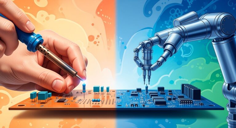
You notice a change when you look at an HDI PCB next to a regular PCB. HDI technology has special things like lots of wires, microvias, and making things smaller. These things help you build electronics that are tiny, light, and quick. Many businesses use HDI because it works well and lasts long. Engineers count on HDI to make new electronic devices better.
Key Takeaways
- HDI PCBs have more wires in a small space. This lets them make more connections. Devices can be smaller and lighter because of this.
- Microvias and special ways of making HDI PCBs help signals stay strong. They also stop signals from getting lost. This makes HDI boards good for fast and tricky circuits.
- HDI technology can make devices 30% to 50% smaller. This helps people make new things like smartphones and wearables.
- HDI PCBs are very dependable. They are tested carefully to make sure there are few mistakes. This is why they are used in cars and medical tools.
- Picking HDI PCBs can make your electronics work better and last longer. You can add more features without making the device bigger.
HDI PCB Basics
What Is HDI PCB
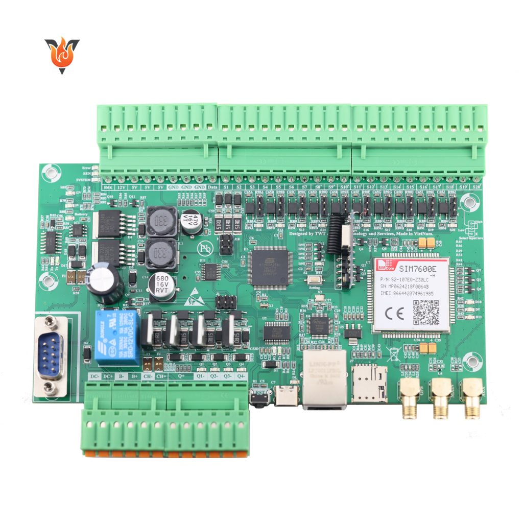
HDI PCB is a special kind of printed circuit board. It fits more wires into a small space than a regular PCB. These boards use very thin lines and spaces, less than 0.10mm wide. The vias are very tiny, usually under 150 micrometers. The capture pads are also small, less than 0.40mm. There are over 20 connection pads in each square centimeter. This high density helps make small and strong devices.
- HDI PCB has more wires in each area.
- Lines and spaces are very thin, at or below 0.10mm.
- Vias are smaller than 150µm.
- Capture pads are under 0.40mm.
- There are more than 20 pads in each cm².
HDI vs. Standard PCB
When you compare HDI and standard PCB, you look at their layers and vias. HDI uses more layers and special vias. Standard PCB has fewer layers and mostly uses through-hole vias. The table below shows the main differences:
| Comparison Factor | HDI PCBs | Traditional PCBs |
|---|---|---|
| Layer Count | More layers, up to 16+ | Fewer layers, usually 6 or less |
| Via Design | Smaller blind, buried, and micro vias | Mostly through-hole vias |
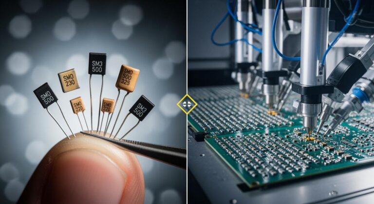
HDI Manufacturing Techniques
HDI boards are made with advanced methods. Laser drilling makes tiny microvias very accurately. mSAP lets you have thinner lines and more layers. FR4 material is popular because it is strong and works well. FR4 will likely be used in over 30% of boards soon. New ideas like microvias and special materials make boards work better. These methods help you build HDI boards that are strong and work well.
- Laser drilling makes tiny microvias.
- mSAP allows thinner lines and more layers.
- FR4 is a good, flexible material.
- New materials and ways make boards better.
Tip: Pick HDI if you want small size and high reliability in your electronics.
Key HDI Features
High Wiring Density
HDI PCBs have a lot more wires in a small space than regular boards. This lets you fit more connections and traces close together. You can make smaller and lighter electronics that still work really well.
- HDI PCBs have more wires and pads in each area than normal boards.
- These boards use blind and buried vias, and often have microvias that are .006 inches wide or less. This makes the circuits even denser.
- You get more wires in each spot than with regular boards.
Because of this, you can add more parts without making your device bigger. The table below shows how having more wires helps your device work better:
| Aspect | Description |
|---|---|
| Wiring Density | More wires in each area than regular PCBs. |
| Signal Integrity | Less signal loss and better electrical performance. |
| Miniaturization | Lets you put more parts in a small space, which is important for new devices. |
| Advanced Features | Helps with complex circuits and fast signals, making your device work better. |
Having wires closer together helps stop signal loss and board problems. HDI can keep signals strong up to 10 Gbps. This makes it great for fast and high-frequency signals.
Microvias and Vias Technology
Microvias and special vias make HDI different from other boards. Microvias connect layers without using much space. They are usually .006 inches wide or less. It is best to use staggered microvias, and only stack two blind steps unless you know taller stacks will work.
- Try to keep the aspect ratio for microvias at 0.75:1 for good strength.
- Always make sure there is enough copper on the side and top of each microvia.
- Make sure the rings around pads are big enough, because small pads can make the board weaker.
Blind and buried vias help you move signals better. Blind vias can make the board 20-30% smaller. In fast circuits, blind vias can lower signal loss by up to 0.5 dB for every inch of wire. You can also fit 50% more wires inside the board compared to just using through-hole vias. Making good microvias needs careful steps, like using the right laser, cleaning well, and making the surface flat.
Finer Lines and Spaces
HDI boards use very thin lines and small spaces. Most HDI boards have lines spaced 3 mil apart. Some special boards can go down to 2 mil/2 mil. Many HDI boards use 4 mil/4 mil as the smallest line and space.
- Thin lines and small spaces let you fit more wires, which helps keep signals strong.
- Smooth copper is needed for thin lines, but it can make the copper stick less to the board.
- If the copper is rough, it can hurt how well signals move, especially at high speeds.
The table below shows how smooth or rough copper changes how easy it is to make fine lines and how strong the copper sticks:
| Fine-line etching | Low roughness (smooth) | Weaker adhesion |
|---|---|---|
| High peel strength | Higher roughness | Harder to etch fine lines |
You need to make sure thin lines will not cause problems when making the board. Thin lines and spaces let you add more features, but you must check if your factory can make them.
HDI PCB Performance Benefits
Signal Integrity
You want your circuit board to send signals quickly and clearly. HDI technology helps by using smart ways to design the board. Microvias and blind vias help keep signals strong. You can also control how signals move on the board. This means you get less noise and fewer problems with crosstalk.
Here are the main problems with signal integrity in high density interconnector designs:
- You have to fit many parts and wires close together. This can make wires cross and signals mix.
- Short and long wires can make signals reach at different times.
- If wires are not sized right, signals can bounce and get weak.
- Power can jump around if you do not plan well.
- Fast signals can lose strength from heat and board material.
- Small parts and tight spaces can make the board hot, which can hurt chips.
You can fix these problems with good HDI design. The table below shows how different choices help electrical performance:
| Design Technique | Improvement in Signal Integrity |
|---|---|
| Optimal Layer Stack-Up | Helps stop interference and makes trace impedance better. It also lowers EMI. |
| Controlled Impedance Routing | Keeps impedance steady for fast signals. This lowers signal loss and reflection. |
| Vias Design and Positioning | Uses microvias and blind vias to keep signals steady. It also stops impedance problems. |
| Noise and Crosstalk Reduction | Adds space and ground planes to keep signals apart. This lowers crosstalk and keeps quality. |
| Proper Power Distribution Network | Keeps noise low and voltage steady. This helps power move better. |
| Considerations for Thermal Management | Fixes heat problems that can hurt signals. It uses thermal vias and good materials. |
Tip: You can keep signals clean and fast by planning your layers and using controlled impedance routing.
Miniaturization
You want your devices to be small and strong. HDI lets you shrink your printed circuit boards by 30% to 50%. For smart wearables, you can make the board over 40% smaller. This means you can fit more features in a tiny space.
You see this in new electronics like smartphones. These devices use HDI boards with 6 to 10 layers. You can put processors, cameras, and sensors all on one board. UHDI technology lets you fit even more in less space. You can make thin devices and still add bigger batteries or extra sensors.
- You can make your device up to half as small.
- You can add more layers and parts without making it bigger.
- You can design new products that were not possible before.
Miniaturization gives you more room to create new things. You can make lighter, thinner, and smarter products for your customers.
Reliability
You need your electronics to work every time. HDI PCB design gives you high reliability. You can trust your board to last longer and work better, even in tough places.
Manufacturers use strict tests to check each board. They use Automated Optical Inspection (AOI), X-ray checks for microvias, and flying probe testing for electrical performance. Top companies keep defect rates below 1%. Most others stay between 3% and 5%.
You also see strong reliability standards in HDI production:
| Metric Type | Description |
|---|---|
| Certifications | ISO 9001 (quality management), ISO 14001 (environmental), IPC-A-600 Class 3 (high-reliability electronics) |
| Inspection Methods | Automated Optical Inspection (AOI), X-ray for microvia strength, flying probe testing for electrical performance |
| Defect Rates | Top manufacturers have less than 1% defect rates. Most others have 3–5% defect rates. |
You get these benefits because HDI uses better materials and careful checks. Your circuit board stays strong, even with high density and small size. You can count on your electronics to work in cars, planes, and medical devices.
Note: High reliability means fewer failures and less downtime for your products.
You see that HDI PCB gives you better signal integrity, more miniaturization, and higher reliability. These benefits help you build advanced electronics that stand out in the market.
HDI PCB Applications
Consumer Electronics
You can find HDI PCB technology in many electronics today. Smartphones and tablets use these boards to work faster and better. More circuits fit in a small space, so your device does more things at once. HDI helps make phones and tablets lighter and thinner. These devices last longer because HDI helps control heat and stops signal problems.
- Your device works better because HDI PCB puts more circuits in less space.
- You get products that are thin and light, so they are easy to carry.
- Your electronics keep working well, even if you use them a lot.
Tip: HDI is used in wearables, smartwatches, and fitness trackers to give you strong features in small gadgets.
Automotive and Aerospace
HDI technology is important in cars and airplanes. Cars use HDI for safety, engine control, and smart driving systems. These boards handle fast data from sensors and other parts. Cars and planes are safer and lighter because of HDI.
- In airplanes, HDI makes small electronics that work in tough places.
- Car makers use HDI PCB to follow safety rules and help electric cars.
- You get boards with many layers that help with smart car checks and self-driving.
Note: NASA and other groups use HDI for new spacecraft, showing how important it is for space.
Medical Devices
Doctors and patients use HDI PCB technology in new medical tools. Wearable and implantable devices use HDI to get smaller and stronger. You get better test results from small machines because HDI keeps signals clear and saves power. Medical tools send data quickly and have less signal trouble.
- HDI helps make small, battery-powered devices for health care.
- You see better test results and safer tools for doctors and patients.
Callout: HDI circuit board technology helps make life-saving tools that fit in your hand or inside your body.
Design and Manufacturing Considerations
Design Challenges
Designing an HDI circuit board is not easy. There are many parts packed close together. This makes it hard to find space for every wire. You need to plan well so wires do not get crowded. If you put parts in the wrong spot, signals can get mixed up. Problems like EMI and crosstalk can happen. Wires might not match up, which hurts how the board works. When parts are close, heat builds up fast. It is harder to keep things cool. Making these boards is tricky. If you do not place things right, layers can be misaligned.
- Not much space makes routing tough.
- Signal problems can cause EMI and crosstalk.
- Heat is harder to control.
- Making mistakes can lead to defects.
The table below shows how HDI boards are different from regular boards:
| Aspect | Standard PCBs | HDI PCBs |
|---|---|---|
| Layer Count | 1 to 12 layers | 6 to 20+ layers |
| Trace Width/Spacing | Larger traces and spacing | Finer traces and spacing |
| Via Types | Through-hole vias | Microvias, blind vias, buried vias |
| Materials | Standard FR-4 | High-performance materials |
| Design Complexity | Simple, lower density | Complex, high density |
Cost and Complexity
HDI boards cost more to start making. You need special tools and materials. This makes the price go up. But if you make a lot of boards, you can save money. Big orders waste less material and take less time. Simple designs help you make more boards faster. Using standard steps makes things quicker and easier. If you pick only the features you need, you can make more boards without problems.
- Starting costs are higher.
- Making lots of boards saves money.
- Simple designs help you make more.
Tip: Choose a maker who knows HDI well to get good boards fast.
Future Trends
HDI boards will be used even more soon. The market will grow a lot by 2025. Smaller and smarter devices need HDI technology. New ideas like AI, flexible boards, and 3D printing are coming. Microvias will help make tiny and powerful products. People want small gadgets, so HDI will keep getting better.
Note: Learning about new HDI trends helps you make better boards for tomorrow.
You notice HDI PCBs are special in today’s electronics. These boards let you put more parts close together. They help signals stay strong and clear. They also help control heat better. You can make smaller devices that work fast and last longer.
- Ultra HDI PCBs let you fit more parts in tiny spaces. This helps you make small products.
- You get better signals with less loss, so things work well.
- Better heat control keeps your devices safe and working right.
Pick HDI PCBs if you want cool features in your next project.
FAQ
What does HDI mean in PCB design?
HDI means High-Density Interconnect. It lets you put more wires and parts on your circuit board. This helps you make smaller and faster devices. Your electronics also become more reliable.
Why should you choose HDI PCBs for your project?
You choose HDI PCBs if you want small, fast, and strong devices. HDI lets you add more features without making things bigger.
Tip: HDI is great for phones, wearables, and smart gadgets.
How do microvias improve your PCB?
Microvias use tiny holes to connect layers. This saves space and makes signals better.
- Microvias let you fit more parts.
- You get less signal loss and better performance.
Are HDI PCBs more expensive than standard PCBs?
HDI PCBs cost more because they need special materials and steps.
| PCB Type | Cost Level |
|---|---|
| Standard PCB | Lower |
| HDI PCB | Higher |
Can you use HDI PCBs in medical devices?
You can use HDI PCBs to make medical devices smaller and stronger. HDI helps you build safe monitors and tools that send clear signals.