How to Achieve the Best PCB Design for Large-Scale Production
You get the best pcb design for big production by thinking about how easy it is to make, making things better, and keeping good quality. If you use DFM rules, you work faster, spend less money, and make printed circuit boards better. Some engineers forget important steps that change how things are made and how they work. For instance, surveys show mistakes like uneven stack-up or missing mechanical details can hurt how things are made and their quality.
| Mistake Type | Description |
|---|---|
| Unbalanced stack-up | Bad stack-up notes can slow down making and cause problems. |
| Trace design mishaps | Trace design errors can break circuits and make building hard. |
| Incorrect via design choices | Wrong via design can mess up signals and how boards work. |
| Overlooked mechanical constraints | Missing mechanical details can cause bad routing and problems. |
| Missing or wrong information | Wrong info in files can slow things down and cause mistakes. |
You can stop these issues by making designs clear, writing good notes, and planning for making things early.
Key Takeaways
- Follow Design for Manufacturability (DFM) rules to make your PCB design easier. This can lower costs, make the quality better, and help finish production faster.
- Plan where you put each component. Make sure there is enough space between parts. This helps stop errors when soldering and putting things together.
- Use the same types of components and materials. Picking common parts makes it faster to get them. It also makes building the PCB less hard.
- Work with your manufacturer early in the design process. This helps find problems soon and makes sure your design works for them.
- Test your prototypes before making many PCBs. Testing early can find mistakes and make your PCB better.
Design for Manufacturability in PCB Production
Why DFM Matters
When you design a pcb for lots of production, you should use dfm rules. These rules help make sure your design works with machines and big batches. Dfm makes building easier and stops problems that slow things down. If you follow dfm, you can find mistakes early and fix them before they cost money.
Dfm rules help keep your design easy to understand. This helps machines build faster and better. Your team can work together well because everyone knows the plan and what to do.
Here is a table that shows why dfm is good for making lots of pcbs:
| Benefit | Description |
|---|---|
| Reduced Production Costs | Dfm lowers costs by making designs simple and cutting waste. |
| Shortened Time-to-Market | Dfm helps move from design to making faster. |
| Improved Product Quality | Simple designs mean fewer mistakes and better products. |
| Increased Production Efficiency | Simple designs help make more boards quickly and well. |
| Enhanced Collaboration | Dfm helps teams work together and reach goals. |
Impact on Cost and Reliability
Using dfm can save a lot of money when making many pcbs. Companies save thousands each year by fixing problems early in design. Dfm stops extra work and wasted parts, so costs stay low and work stays on time.
Reliability is also very important with dfm. If you use dfm, your pcb is strong for machines and tough places. Good part placement helps control heat and makes solder joints stronger. In big production, this means your boards can handle shaking and stress without breaking.
- Dfm fixes problems like tight spaces and wrong pad sizes.
- Good layout and spacing help machines build better and cut mistakes.
- Using dfm makes sure your pcb is always high quality.
By using dfm, you work faster, spend less, and make sure your pcb is strong for big production.
Key Principles of Best PCB Design
Component Layout and Clearance
It is important to put parts in the right places. You need to leave enough space between traces and parts. This helps stop mistakes when making the pcb. Soldering is easier if there is enough room. Short circuits are less likely to happen. The ‘3W principle’ helps set the right space between traces. For high voltage, you should make the space bigger. Use insulation to keep high and low-voltage parts safe.
Industry standards help you make good choices. IPC-2221 gives rules for heat and trace width. IPC-9592 tells you how far apart power devices should be. Here are some important standards:
| Standard | Description |
|---|---|
| IPC-2221 | Details requirements for thermal management and trace width to prevent overheating. |
| IPC-9592 | Establishes safety standards for power conversion devices, guiding spacing based on voltage. |
Do not use sharp corners in traces. Curved traces are better for signals. Always check the space between parts when planning your layout. This helps with dfm and makes your pcb ready for big production.
Standardization for Manufacturability
Using common parts is very important for big production. Standard parts make building faster and easier. This lowers risk and helps make more boards. Try not to use rare or custom parts. These can slow down buying and cost more money.
Standard materials and resistor values help you get parts faster. Here are some reasons why standardization is good:
| Benefit | Explanation |
|---|---|
| Faster Procurement | Standard materials are readily available, which shortens the time needed for material sourcing. |
| Reduced Manufacturing Complexity | Using standard materials simplifies processing and reduces setup time for manufacturing equipment. |
- Standard materials ship faster than special ones.
- Relaxed tolerances help avoid slowdowns in making.
- Panelization lets you make more boards at once.
- Good design files stop dfm problems.
By using dfm and standard parts, you help your layout and keep production on time.
Proper Dimensions and Spacing
You must check sizes and spaces for a good pcb. Wrong footprints can make parts not fit right. Bad solder joints can happen if things are not lined up. Trace width and space stop shorts and crosstalk. Always use industry rules for your design.
Here are some spacing rules for different classes:
| Standard | Class 1 & 2 Minimum Spacing | Class 3 Minimum Spacing | Additional Notes |
|---|---|---|---|
| J-STD-001 | 0.25mm (10 mil) | 0.18mm (7 mil) | Minimum spacing of 1.5mm (60 mil) between components and adjacent traces. |
| MIL-PRF-55110 | 0.25mm (10 mil) | 0.15mm (6 mil) | Spacing increases for higher voltage levels based on insulation requirements. |
| IPC-2221 | 0.25mm (10 mil) | 0.5mm (20 mil) | Minimum creepage and clearance distances specified for Class 3 PCBs. |
| IPC-2221A | N/A | N/A | Specific guidelines for high-speed digital signals to ensure signal integrity. |
| IPC-2222 | 0.25mm (10 mil) | 0.15mm (6 mil) | Guidelines based on voltage levels and current carrying capacity. |
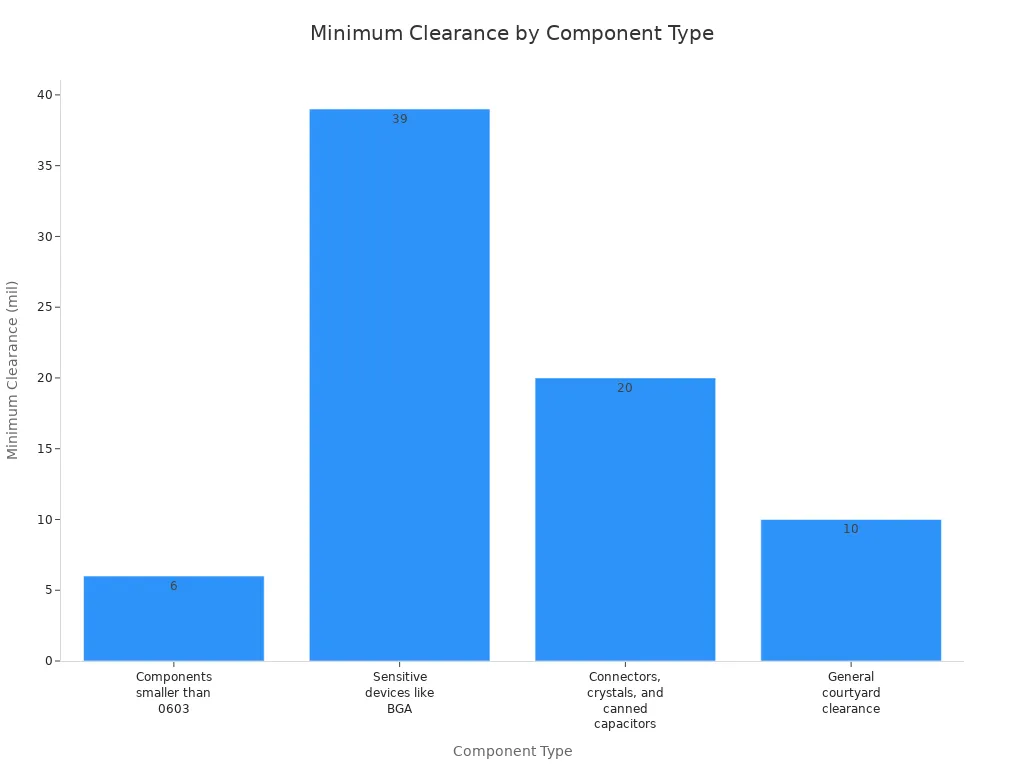
Use these clearances for different parts:
| Component Type | Minimum Clearance |
|---|---|
| Components smaller than 0603 | 6 mil |
| Sensitive devices like BGA | 39 mil |
| Connectors, crystals, capacitors | 20 mil |
| General courtyard clearance | 10 mil |
- Keep at least 8 mil between parts and holes.
- Leave 7 mil from pad to annular ring edge.
These steps help stop problems and follow dfm rules. Good spacing also helps signals and makes panelization easier.
Layer Stackup and Copper Weight
Layer stackup and copper weight are important for good pcb design. Start by thinking about what your pcb needs. Think about signal speed, power, and where it will be used. Count how many layers you need for all the pins and routes. Use good tools to plan your stackup and check impedance.
Pick the right substrate and copper foil for your board. Talk to your manufacturer early to see what they can do. Test your stackup with simulations and prototypes. Pick copper weight that matches your current needs. Use thick copper for power designs to carry more current. Use thin copper for fast signals to keep losses low.
Follow these tips:
- Make ground layers thick enough for return currents.
- Add more layers to help with noise and power.
- Put a solid ground under important signals for better quality.
- Simulate your design before making it.
- Check if your manufacturer can use special copper weights.
- Thick copper needs wider traces, which can make layouts harder.
Doing these things helps with dfm, makes your pcb better, and keeps production fast. Good stackup and copper weight also help with panelization and make building easier.
PCB Layout and Component Selection
High-Speed Component Placement
You must think carefully about where high-speed parts go. In big production, trace routing affects how signals move. If you put parts randomly, signals can get weak. This can cause delays and problems. Use dfm rules to keep signals strong. Engineers test and simulate to find issues like crosstalk. Good placement keeps signals safe and makes your design work well.
Tip: Always look for delay, impedance matching, and crosstalk when placing high-speed parts. This helps keep your pcb working well.
Grouping Interacting Components
You can make your layout better by putting parts that work together close. This helps you follow dfm rules and makes building easier. Logical groups mean fewer changes and faster production. Put surface mount devices on one side of the board. This makes building quicker and costs less.
| Strategy | Description |
|---|---|
| Group Components into Rooms | Put related parts together to manage traces and reduce changes. |
| Design Simplification | Keep your design simple to make building easier and cheaper. |
| Logical Layout Organization | Organize your layout so assembly is easy and yield is high, like grouping SMD parts. |
Use dfm rules to pick good materials and make traces better for building.
Material Selection for Reliability
Picking the right materials helps your pcb last longer in big production. Epoxy resin is strong and works for most boards. For HDI pcbs, use I-Speed or I-TeraMT40. These help your design stay good and last longer. Always check if your materials meet RoHS and REACH rules. Do not use parts that are old or not good for new designs. This keeps your production smooth and your pcb strong.
| Material | Characteristics | Recommended Use |
|---|---|---|
| Epoxy Resin | Cheap, strong, good for most boards | Industry standard |
| I-Speed | Good for HDI boards, handles complex designs | HDI PCBs |
| I-TeraMT40 | Reliable for high-density interconnects | HDI PCBs |
| OhmegaPly | Very reliable for advanced boards | HDI Boards |
If you use dfm rules and make smart choices, you can make your pcb better, stronger, and more reliable every time.
Avoiding Common PCB Design Mistakes
Overcomplicated Layouts
Some people think more features make a pcb better. But adding too many layers can cause problems. Complex layouts cost more money and lead to mistakes. Using lots of layers or rare parts makes building harder. This slows down how fast boards get made. It also means more defects can happen. The table below shows how complexity changes your project:
| Factor | Impact on Costs and Defect Rates |
|---|---|
| Design Complexity | Bigger parts and special orders cost more money. |
| Layer Count | More layers need extra materials and slow production. |
| Non-standard Components | Special parts need new steps, which causes errors and costs. |
| Trace Widths | Thin traces need fancy tools, so making costs go up. |
| Via Diameters | Tiny vias need special drills, which costs more. |
| Manufacturing Complexity | Extra layers and steps mean more mistakes can happen. |
You can stop these issues by keeping your layout simple. Use regular parts and do not add too many layers. This helps you save money and make better boards.
Ignoring Manufacturer Capabilities
If you do not check what your builder can do, you may have problems. Every builder has limits for things like trace width and layer count. If you ignore these limits, you might need to change your design later. Sometimes, your boards may not work at all. Here are some things that can go wrong:
| Consequence | Description |
|---|---|
| Increased Costs | Fixing mistakes or rushing orders costs more money. |
| Delays in Production | Hard designs slow down every step of making. |
| Design Failures | Not testing can make boards break more often. |
| Complications in Sourcing Components | Rare parts are hard to find and slow things down. |
| Reputational Harm | Bad designs can hurt your company’s name. |
- Making designs too hard slows down building.
- Changing designs at the last minute adds risk.
- Using dfm rules helps you find and fix problems early.
Always talk to your builder before you finish your design. This makes sure your pcb matches what they can do and keeps things running smoothly.
Poor Documentation
Good notes and drawings help make boards right. If you forget details, people get confused and make mistakes. More than half of new designs get delayed because notes are not clear. This can slow down your project and cost more money. Good documentation means you include drawings, lists, and instructions.
- Bad notes cause confusion and mistakes.
- Always give full and clear files to keep things moving.
When you write clear notes, everyone knows what to do. This helps your project stay on track and makes your pcb better.
Practical Tips and Tools for Manufacturability
DFM Checklists and Software
You can make your pcb easier to build by using DFM checklists and software. These tools help you spot problems early in your design. If you use them, you save time and avoid expensive mistakes. Many engineers use DFM software before sending their design to be built. This step helps you follow dfm rules and get your pcb ready for making.
| Software Tool | Description |
|---|---|
| DFMPro | Finds problems early, saves time, and cuts down on fixing. |
| DFMExpress | Works with CAD programs and gives quick feedback. |
| DFMNow | Free Gerber viewer with DFM checks for building. |
| PCBflow | Checks if your pcb and assembly are easy to make. |
| VayoPro-DFM Expert | Gives reports and checks for building and assembly. |
| Altium Designer | Professional pcb design tool with DFM features. |
| Autodesk Fusion 360 | Cloud platform with design, testing, and building tools. |
| SolidWorks | 3D CAD tool with DFM checks for building and assembly. |
| Inventor | Helps with DFM checks for strong designs. |
| Creo | Advanced DFM and design tools for checking parts. |
Tip: Use DFM software to find mistakes early and get quick feedback. This keeps your quality high and stops delays in making.
Early Collaboration with Manufacturers
You should talk to your builder early when you start your design. This helps you find problems before they get big. Working together lets you pick better parts and spend less money. Early teamwork helps you change your design so it is easier to build and lasts longer.
- You can find limits and hard-to-get parts early.
- Small changes at the start can save money and make your pcb stronger.
- Working together on dfm checks helps you stop slowdowns in making.
Note: Early talks with your builder help you fix problems before they slow down making. Teamwork leads to better designs and smoother building.
Prototyping and Feedback
Making a prototype is important for good quality and better designs. When you build and test a sample, you can find mistakes before making lots of boards. Early tests help you check for problems like wrong vias or bad solder joints. Studies show that testing can lower mistakes by 30-50%. For example, one company found a via problem during testing and stopped thousands of bad boards.
- Test your design with a sample to find mistakes early.
- Use feedback from tests to make your pcb easier to build and stronger.
- Change your design based on real results to keep your pcb ready for making.
Remember: Testing and feedback help you follow dfm rules and get the best pcb design.
You can get the best pcb design for big production by using dfm, making things easy to build, and working well with others. Dfm helps you spend less money, make boards faster, and keep them strong. You should put parts in smart places, use the same soldering steps, and check your design with dfm before you finish. Working with builders early and getting feedback helps your pcb get ready for making.
| Principle | Description |
|---|---|
| PCB layout | Put parts in good spots and keep away from the edges. |
| Signal integrity | Draw traces carefully so signals stay strong. |
| Thermal management | Control heat to make boards last longer. |
| Mechanical considerations | Spread out stress so boards do not break. |
To keep getting better, look at guides about making pcbs, picking materials, and learning IPC rules.
- Top DFM and DFA Mistakes that Delay Your PCB Production
- PCB Manufacturing Process
- PCB Material Selection
- PCB Stack-Up Resources
- PCB IPC Standards Resources
- How to Optimize Your PCB Prototype for Production
- Ready to Scale? Time to Optimize Your PCB Design
FAQ
What is the most important factor for PCB mass production?
You need to think about manufacturability. DFM helps you stop errors and slowdowns. DFM makes your design simple to build and test. This means you get faster production and better boards.
How can you avoid common PCB design mistakes?
Use a DFM checklist and look over your design files. Always check space, where parts go, and your notes. Getting feedback from your manufacturer early helps you find mistakes before making starts.
Why should you standardize components in your design?
Standard parts make building your PCB easier. You get parts faster and spend less money. Manufacturers can find standard parts quickly. This helps you avoid delays and finish your project on time.
When should you talk to your PCB manufacturer?
Talk to your manufacturer early when you start your design. Early talks help you learn what they can do. You can change your design to fit their process and avoid expensive changes later.