You might feel unsure when you start to design your first pcb circuit board. Many new people have problems like putting parts in the wrong place or forgetting important test points. You should learn basic pcb words before you start. You will make mistakes, but you can fix them and get better. The table below shows common problems and ways to help you avoid trouble as you go from your idea to a working board.
| Challenge | Problem | Solution |
|---|---|---|
| Improper Component Placement | Bad layouts, signal noise | Put parts in a smart order |
| Power and Ground Design Issues | Circuit does not work well | Use strong ground planes |
| Poor Routing Practices | Signal problems | Do not use sharp angles, keep good spacing |
| Soldering Issues | Weak solder joints, short circuits | Use the right way to solder |
PCB Circuit Board Basics
PCB Composition
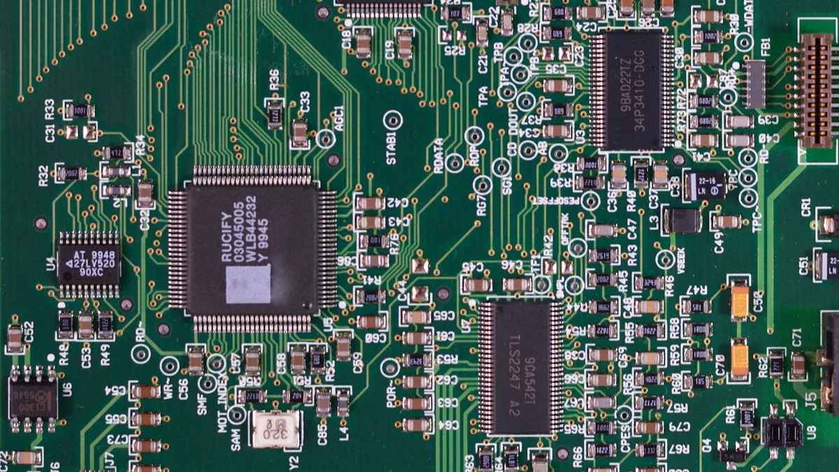
Before you start pcb design, you should know what is inside a pcb circuit board. A printed circuit board has different layers and materials. Each layer does something important. The core makes the board strong. It also stops electricity from leaking out. Most cores use FR-4. FR-4 is tough and safe. Some boards use polyimide. Polyimide works well with heat or when the board needs to bend.
Here is a table that shows the main layers and what they do:
| Layer Type | Description |
|---|---|
| Core | Solid, nonconducting base laminated with copper. |
| Copper Foil | Conductive layer for circuit designs. |
| Signal Plane | Carries electrical signals between components. |
| Power Plane | Distributes power supply voltages. |
| Ground Plane | Provides a return path for electrical currents. |
| Prepreg | Dielectric material that isolates and binds layers. |
| Routing Layer | Routes electrical traces between components. |
| Copper Pour | Copper-filled areas for extra conductivity. |
Most printed circuit boards have these layers. Each layer helps your board work well. They also help your board last a long time.
Key PCB Terminology
When you begin pcb design, you will see new words. Learning these words helps you read guides. It also helps you use design software. Here are some words you will need:
- Trace: Thin copper lines connect parts on the pcb.
- Via: Small holes link layers of the board.
- Pad: Metal spots let you solder parts onto the pcb.
- Silkscreen: Printed labels show where parts go.
Tip: If you know these words, you can talk about pcb design with others. You will not get confused.
You will use these words every time you work on a printed circuit board. Knowing them makes your work easier. It also helps you find mistakes early.
Step-by-Step Guide to PCB Design
Making your first pcb circuit board can seem hard. This guide will show you each step. You will learn how to set goals, pick parts, and use good schematics. Each step helps you feel more sure. You will also avoid mistakes in pcb design.
Define Project Goals
Start every pcb project with a clear goal. This guide helps you set strong goals for your pcb:
- Ask everyone in your project what they need.
- Find out what your pcb circuit board will be used for.
- Decide what you want your circuit to do.
- Think about how well your circuit should work.
- Know if you have limits like space or power.
- Plan your budget and how much time you have.
- See if you need to follow any safety or market rules.
Tip: Write your goals down. This helps you stay on track. You can use your goals to help you make choices as you design.
Select Components
Picking the right parts is important for pcb design. Your parts should match your project goals. The table below shows what to look for when you pick parts for your pcb:
| Criteria | Description |
|---|---|
| Electrical Specifications | Make sure parts match your circuit needs, like voltage and power. |
| Size and Package Type | Think about the size and how parts will be put on the board. |
| Availability and Cost | Pick parts that are easy to find and fit your budget. |
| Environmental Factors | Choose parts that work well in your board’s conditions, like heat or moisture. |
| Manufacturer Reliability | Buy parts from good suppliers so you do not get bad parts. |
Always check if your parts are easy to buy and not too expensive. Using common parts makes your pcb easier to build and fix.
Gather Reference Schematics
Reference schematics help you design your pcb with less worry. Schematics are like maps for your circuit. They show how to connect each part and help you not make mistakes. You can find good schematics from products and designs made by chip companies. These designs are tested, so you know they work.
Schematics also help you see how your pcb circuit board will work. They help you make Gerber files, which are needed to build your pcb. When you use reference designs, you learn the right way to use main parts. This makes your guide better and helps you learn good ways to design your pcb.
Note: Always make sure your schematic comes from a trusted place. This helps you avoid problems later when you design.
If you follow this guide, you will start your pcb project well. You will make better choices and build a pcb circuit board that works how you want.
PCB Board Design Software
Choosing the Right Software
You need to pick the best pcb board design software for your first project. Many tools help you create and test your pcb. Some popular choices include:
- Altium Designer offers powerful features for professionals.
- EAGLE is easy to use and works well for beginners.
- KiCad is free and open-source, perfect for hobbyists.
- OrCAD suits advanced engineers.
- Proteus helps with simulation and learning.
- EasyEDA is web-based and great for group projects.
When you choose pcb design software, look for features that match your needs. The table below shows what to consider:
| Feature | Description |
|---|---|
| Ease of Use | Simple tools and tutorials help you learn quickly. |
| Support and Community | Active forums and guides solve problems fast. |
| Key Software Features | Simulation and testing tools check your pcb board design. |
| Component Libraries | Large libraries save time when you add parts. |
| File Compatibility | Standard formats make manufacturing easier. |
| Collaboration Features | Cloud tools let you work with others. |
| Free Trials and Demos | Try before you decide. |
| Future-Proof Your Choice | Pick software that grows with your skills. |
Tip: Define your project scope, set your budget, and think about how you want to access your software.
Setting Up Your Tool
After you choose your pcb design software, you need to set it up. Follow these steps to start your pcb board design:
- Choose and install your software.
- Create your schematic by adding and connecting parts.
- Move to the pcb layout and arrange components.
- Route traces to connect everything.
- Finalize and export your design files.
- Review your work and order your pcb.
You should check each step for mistakes. Good setup helps you avoid problems later.
KiCad for Beginners
KiCad makes pcb board design easy for new users. You get open-source software with no cost. KiCad supports both schematic and pcb design in one place. You can use tools like a pcb calculator, Gerber viewer, and 3D viewer. These features help you see your design and fix errors before you build your pcb.
Note: KiCad has a friendly community and many guides. You can learn quickly and get help when you need it.
KiCad gives you everything you need to start pcb design. You can build your first pcb board design with confidence.
Create the Schematic
When you start pcb design, you need to create the schematic. This step helps you plan how each part connects. You use software to draw your circuit before you build the board. A good schematic makes your pcb easier to build and test.
Add Components
You begin by adding all the parts your circuit needs. Most pcb design software follows these steps:
- Create a new schematic file.
- Place each component on the schematic. Change the names and footprints so they match the parts you will use on your pcb.
- Link the schematic to the netlist. The netlist is a list of all the connections in your circuit.
- Start a new pcb project. Add both the schematic and pcb files to your project.
- Use the update tool to check if your schematic and pcb files match.
- Let the software compare the connections. Change your schematic if you find mistakes.
Tip: Place parts in a way that makes the circuit easy to read. Group related parts together.
Connect Wires
After you add components, you need to connect them with wires. Good wire connections make your schematic clear. Use these best practices:
| Best Practice | Description |
|---|---|
| Organization | Arrange wires neatly and label them to show their purpose. |
| Colours | Use different colors for wires like power, ground, or signals. |
| Terminations | Show clear connections with dots where wires meet parts. |
| Net label Routing | Use net labels to reduce clutter and show connections without extra wires. |
| Use Grid Snap | Turn on grid snap for straight and tidy lines. |
Note: A neat schematic helps you find errors and makes your pcb design process smoother.
Schematic Error Check
Before you move to the pcb layout, check your schematic for mistakes. Look for these common errors:
| Error Type | Description |
|---|---|
| Connectivity Errors | Check for pins that are not connected or wires that are shorted by mistake. |
| Missing Decoupling Capacitors | Make sure you add decoupling capacitors near power pins of chips to prevent noise. |
| Incorrect Component Values/Types | Double-check that you use the right values and types for resistors, capacitors, and other parts. |
- Make sure each voltage has a power source with a clear net name.
- Check that all power pins connect to the right voltage.
- Review all grounds and confirm each one has a ground source.
Tip: Careful checking now saves you time and money later.
You can now move to the next step in pcb design with confidence. A clear schematic helps you build a pcb that works well.
Convert Schematic to PCB Layout
After you finish your schematic, you need to define the pcb layout. This step turns your circuit diagram into a real board that you can build and use. You will work through assigning footprints, setting the board size and shape, and arranging your components for the best results.
Assign Footprints
You must link each part in your schematic to a physical shape, called a footprint, on the pcb layout. This step helps your design tool know where to place pads and holes for each component. Follow these steps to assign footprints:
- Learn the footprint naming rules in your design software, such as KiCad.
- Make a new pcb library to store your footprints.
- Add new footprints and set their properties in the Properties panel.
- Build a schematic library to keep your symbols.
- Match the pin numbers on your symbol to the pad numbers on your footprint.
Tip: Double-check that every pin lines up with the right pad. This prevents errors when you build your pcb.
Board Size and Shape
The size and shape of your pcb layout affect how well your board works and how easy it is to make. You should plan this early in your design process. The table below shows how different factors matter:
| Factor | Description |
|---|---|
| Routing and Spacing | Good spacing keeps signals clear and makes the board easier to build. |
| Custom PCB Sizes | Custom shapes give you options but can make design and manufacturing harder. |
| Electrical Properties | Bigger boards let you use wider traces, which lowers resistance and boosts conductivity. |
| Thermal Management | Large boards spread out heat better, so your parts stay cool. |
| Layer Stackup Planning | Careful planning of layers saves space and improves how your circuit works, especially for complex boards. |
Note: Always check your board outline before you start placing parts.
Component Placement
Smart component placement makes your pcb layout easier to build and helps your circuit work better. Use these steps for the best layout:
- Place large or high-pin-count parts first. These need more space and often have smaller parts around them.
- Keep digital and analog parts apart. This stops fast signals from causing noise in sensitive areas.
- Put clock drivers close to oscillators. This reduces signal problems and keeps timing accurate.
- Arrange parts in a logical order. This saves space and helps avoid mistakes during assembly.
- Leave at least 1 mm between parts and 2.5 mm from the board edge. This prevents errors when making the pcb.
- Place decoupling capacitors near power pins to keep power stable.
You should also:
- Set the board outline in your design tool first.
- Place connectors on the edge of the pcb layout.
- Put protection parts near connectors.
- Group power parts away from sensitive analog or RF areas.
Remember: Careful placement now saves time and trouble later.
PCB Trace Routing
Routing is an important part of pcb design. You must connect all the parts with copper traces. Good routing helps your circuit work well. It also makes building the board easier. You can use manual routing or auto-routing. Each way has good and bad points.
Manual vs. Auto-Routing
Manual routing lets you pick where every trace goes. You control each wire on your pcb. This way feels good, especially for hard circuits. You get to be creative, but it takes longer. Auto-routing uses software to connect the traces for you. It follows the rules and works quickly. Auto-routing is best for big or crowded boards. You still need to check important spots.
Here is a table that shows both ways:
| Method | Advantages | Disadvantages |
|---|---|---|
| Manual Routing | Creative control, fun for complex circuits | Time-consuming, less efficient for big boards |
| Auto-Routing | Fast, follows design rules | Needs oversight, not perfect for every board |
Tip: Use manual routing for small boards. Try auto-routing for bigger ones, but always check the work.
Avoiding Routing Mistakes
You can stop routing mistakes by following easy steps. Many problems happen if traces are too close or too thin. Plan your routing before you begin.
- Leave enough space between traces. This stops noise and cross-talk.
- Pick the right trace width for each signal. Strong signals need wider traces.
- Make sure vias are the right size. Small vias can break or cause trouble.
- Put decoupling capacitors near IC pins. This helps power get to the parts.
- Route traces from surface mount devices with care. Do not block the paths for other traces.
- Use design tools to check trace width and spacing.
- Leave enough room for routing, especially in tight spots.
- Use standard footprints for pads. This stops solder from joining pads by mistake.
- Use a solid ground plane to lower noise.
Note: Careful routing makes your pcb design better and stronger. You will save time and not make expensive mistakes.
Power and Ground Planes
Adding Planes
You need to add power and ground planes to your pcb layout to help your circuit work better. These planes are large areas of copper that cover parts or all of your board. They give your components a stable place to get power and return signals. You can follow these steps to add power and ground planes in your pcb design:
- Minimize the area where current loops travel. This helps control noise and keeps your signals clean.
- Place power and ground planes next to each other in the layer stack-up. This reduces electromagnetic interference (EMI).
- Use thin dielectric material, about 0.1–0.2 mm, between these planes. Thin layers increase capacitance and improve high-frequency decoupling.
- Make sure every signal layer has a continuous reference plane, usually a ground plane, above or below it.
Tip: Keep your ground plane as one solid piece. Do not split it. This keeps your signals strong and stable.
Here is a table that shows best practices for power and ground planes:
| Best Practice | Description |
|---|---|
| Layer Stack-Up | Power and ground planes should be adjacent to each other to reduce EMI. |
| Power Plane Size | Extend power planes to cover the entire PCB for low impedance and less voltage drop. |
Why Planes Matter
Power and ground planes play a big role in your pcb. The ground plane acts as a universal reference point for all signals. It gives a low-impedance path for return currents. This keeps voltage levels steady and helps your circuit avoid noise.
- The ground plane should be the most stable and complete layer in your pcb.
- Always keep at least one continuous ground plane in multilayer boards.
- Avoid splitting the ground plane. This keeps your signals safe and strong.
Power and ground planes also help with power delivery. They create a low-impedance network, which means less voltage fluctuation. Your components get steady power, even when the current changes quickly.
- These planes help with electrical and thermal management.
- They improve signal integrity and reduce EMI.
- Your pcb design will work better and last longer when you use strong power and ground planes.
Note: Good power and ground planes make your pcb more reliable. You will see fewer problems with noise and voltage drops.
Silkscreen and Markings
Silkscreen and markings help people know where parts go on your pcb. These printed labels show you how to place each part. Good silkscreen makes building, testing, and fixing your pcb easier.
Labeling Components
You should put clear labels on your pcb silkscreen. This helps you not make mistakes when you build or check your board. Here is a table that lists what you should add:
| Information to Include in Silkscreen and Markings |
|---|
| Reference designator for each component |
| Component values for passives |
| Pin-1 indicator for ICs |
| Polarity indicators for power and ground |
| Component outlines where needed |
| Part numbers for the assembly |
| Company and manufacturer logos |
| Serial and lot numbers |
| Regulatory markings |
| Connector pinouts |
| Notes for assembly, testing, or operation |
Always mark which way capacitors and diodes go. Show the first pin on connectors and ICs. Draw outlines for big or special parts. Add your company logo and part number if you want to keep track of your boards.
Tip: Clear silkscreen labels help you find problems and fix them quickly.
Best Practices
You can use these tips to make your silkscreen easy to read:
- Use lines at least 4 mils wide so words print well.
- Leave at least 6 mils between silkscreen and copper traces.
- Do not let silkscreen touch pads or traces.
- Put labels so you can read them easily on the board.
- Make sure each label matches the right part.
- Mark which way polarized parts go and how they face.
- Use mechanical layers for logos or pictures not needed for building.
- Mirror the bottom layer labels so they read the right way.
- Keep silkscreen away from RF traces to stop signal trouble.
- Label parts with many pins and show pin numbers for easy checking.
Do not put silkscreen under small parts. This can make soldering hard. Always check your board name, part number, and revision to make sure they are right.
Note: Good silkscreen and markings help everyone build and use your pcb without problems.
Design Rule Check (DRC)
Running DRC
You need to run a Design Rule Check before you finish your pcb design. This step helps you find mistakes that could cause your pcb to fail. Most pcb design software has a DRC tool that checks your board against a set of rules. You set these rules based on your project needs and manufacturing limits.
Here are the most important rules you should check:
- Minimum clearance between traces and pads to prevent short circuits.
- Trace width to make sure each trace can carry enough current without overheating.
- Proper component placement for good heat flow and signal quality.
- Via sizes and spacing to keep connections strong and reliable.
- Solder mask clearance to stop solder from bridging and causing shorts.
When you run DRC, the tool scans your pcb and lists any problems. You see warnings for things like traces that are too close, pads that overlap, or copper too near the board edge. You also get alerts for signal integrity issues in high-speed designs.
Tip: Always run DRC after every major change in your design. This helps you catch errors early.
Fixing Errors
You will find errors when you run DRC. Fixing these errors makes your pcb safe and ready for manufacturing. Common problems include:
- Inadequate trace widths that cannot handle the needed current. You should set trace width rules based on standards.
- Insufficient spacing between traces, which can cause shorts. Enforce minimum spacing rules in your design tool.
- Overlapping pads and vias that lead to solder bridges or bad connections. Set clearance rules for pads and vias.
- Annular rings that are too small, risking broken connections. Define a minimum annular ring size.
- Solder mask misalignment, which exposes copper or causes solder bridges. Make sure you set correct mask clearance.
- Silkscreen overlaps that interfere with soldering. Prevent silkscreen from covering pads or traces.
- Incorrect net connections that create unwanted shorts or open circuits. Compare your netlist with the layout.
- Poor component placement that makes assembly or inspection hard. Set spacing rules for components.
You should fix each error by following the suggestions from your design software. After you correct the problems, run DRC again to confirm your pcb is error-free.
Note: Careful DRC and error fixing help you build a reliable pcb that works as planned.
Gerber Files for PCB Manufacturing
When you finish your pcb design, you need to create Gerber files. These files tell the manufacturer exactly how to build your pcb. Gerber files use a special format that shows every layer of your board. You include details like copper traces, drill holes, solder masks, and silkscreen images. Manufacturers use these files to make sure your design becomes a real, working pcb.
Gerber files are open ASCII vector format files. They describe each physical layer of your pcb. You see objects like copper traces, vias, pads, and silkscreen images. Each object uses a flash or draw code and vector coordinates.
Gerber files help manufacturers around the world work together. They make the process faster and more accurate. You avoid mistakes and get a pcb that matches your design.
Exporting Gerber Files
You need to export Gerber files from your pcb design software before you send your board for manufacturing. Each software has its own steps. Here is a simple guide you can follow:
- Open your pcb layout in your design software.
- Go to the menu bar and find the export option for Gerber files.
- Choose the layers you want to include, such as copper, solder mask, and silkscreen.
- Set the parameters for line width and other details.
- Click the button to create the Gerber files.
- Rename the files so the manufacturer knows which layer each file represents.
You should always check the settings before you export. This helps you avoid missing important layers or details.
File Review
After you export your Gerber files, you need to review them. Use a Gerber viewer to open each file. Look for missing traces, wrong drill holes, or misplaced silkscreen markings. Make sure every layer matches your original design. If you find mistakes, go back to your pcb design software and fix them.
- Check copper layers for complete connections.
- Confirm drill files match your component holes.
- Review silkscreen for clear labels and correct placement.
Tip: Careful review of your Gerber files helps you avoid costly errors during manufacturing.
When you finish your review, you can send the files to your manufacturer. You know your pcb will match your design and work as planned.
PCB Manufacturing Process
Choosing a Manufacturer
You need to pick a manufacturer who can make your pcb circuit board. The right choice helps you avoid problems and waiting. Different manufacturers offer different help and services. You should think about a few things before you choose. Here is a table that shows what to look for:
| Criteria | Description |
|---|---|
| Material Handling Capabilities | Can the manufacturer work with the materials your pcb circuit board needs? |
| Surface Finish Options | Do they offer finishes like HASL, ENIG, or OSP for better soldering and durability? |
| Quality Standards and Certifications | Do they have certifications such as ISO 9001 or IPC for reliable quality? |
| Geographic Considerations | Is the manufacturer close to you for faster shipping and easier communication? |
| Communication and Customer Service | Will you get quick answers and good technical support? |
| Pricing Structure | Do you understand their pricing for your board size and features? |
| Scalability and Production Volume | Can they handle more boards if your project grows? |
| Lead Time and Delivery | How fast can they make and ship your pcb? |
Tip: Ask for sample boards or talk to other customers. Good support and clear answers make your project go smoother.
Submitting Files
After you pick your manufacturer, you need to send your design files. Most manufacturers want Gerber files, drill files, and a bill of materials. You should check your files for mistakes before you send them. Use a Gerber viewer to make sure your pcb looks right. Clear files help the manufacturer build your board without errors.
- Get your Gerber files ready and check each layer.
- Include drill files for holes and vias.
- Add a bill of materials with part numbers and values.
- Write notes if you have special instructions.
Note: Always check your files before sending them. Mistakes in your files can slow things down or cause bad boards.
What Happens Next
After you send your files, the manufacturer starts making your pcb. There are many steps before you get your finished board. Here is what usually happens:
- Pre-production engineering checks your files for mistakes and gets them ready.
- Inner layer imaging uses lasers to make the circuit pattern.
- Etching takes away extra copper, leaving only the needed traces.
- Design verification checks if your files match the rules.
- Material preparation picks the right base and copper layers.
- Imaging and etching put your design onto the copper.
- Drilling makes holes for vias and parts.
- Plating connects the layers with metal.
- Solder mask and silkscreen add protection and labels.
- Testing checks your pcb for electrical problems.
🛠️ You can ask your manufacturer for updates during these steps. Most companies will tell you how your board is doing and let you know if there are any problems.
When the process is done, the manufacturer ships your pcb circuit board to you. You can then put your project together and test it.


