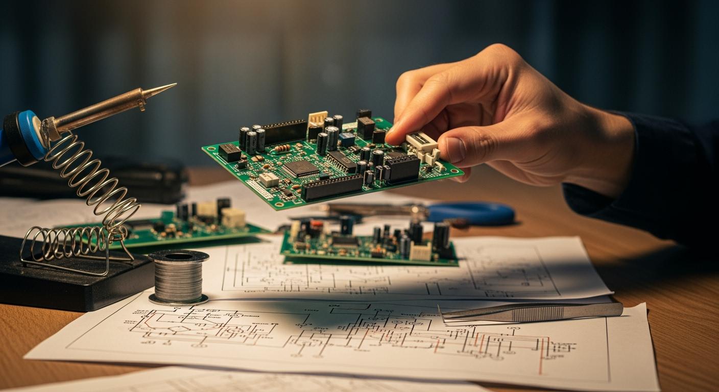
Imagine starting a pcb assembly project without a schematic diagram. You might place components in the wrong spots or connect traces incorrectly. A schematic gives you a clear map to follow during design and assembly. This diagram shows how each part works with others, so you avoid costly mistakes. You need the schematic diagram to check every connection and make sure your design matches the function you want. Without a good schematic, your diagram will confuse you and lead to errors.
Key Takeaways
- Schematic diagrams serve as essential blueprints for PCB assembly, guiding the placement and connection of components.
- Standardized symbols in schematics enhance clarity, making it easier for teams to understand and follow the design.
- Using automated checking tools can catch errors early, preventing costly mistakes during the assembly process.
- A well-organized schematic improves communication among designers and technicians, leading to a smoother assembly experience.
- Double-checking your schematic before moving to layout ensures accuracy and saves time during the design and assembly phases.
Why Schematic Diagrams Matter in PCB Assembly
Foundation of PCB Design
A schematic diagram gives you the foundation for every pcb assembly project. You use this diagram to see how each electrical part connects and interacts. The schematic shows you the logic behind the circuit, making it easier to understand the design and the pcb layout. When you start the design process, you rely on the schematic to organize components and plan the pcb layout. This step helps you avoid confusion and ensures that your pcb design matches the intended functionality.
A well-made schematic diagram acts as a blueprint. You can document every component and their relationships. This visual map helps you keep track of the design process and makes the pcb layout more accurate.
You benefit from standardized symbols and clear connections in the schematic. These features make the diagram easy to read and share. When you work with others on pcb assembly, everyone can follow the same schematic and understand the design. You use the schematic to guide the placement of parts and the routing of traces in the pcb layout. This approach helps you build a reliable pcb and reduces mistakes during the design process.
- Schematic diagrams provide a visual representation of electrical circuits.
- They use standardized symbols and connections, making it easier to understand the circuit’s function.
- They serve as a blueprint, ensuring accurate documentation of components and their relationships.
- Schematic diagrams illustrate how electrical components are interconnected.
- They facilitate the design, testing, and building of circuits.
- A solid understanding of electrical schematics is essential for creating effective PCBs.
You also use the schematic diagram to communicate with assembly technicians. The diagram gives a clear graphical view of the circuitry, which helps everyone understand the pcb layout and the design process. Good organization in the schematic, such as grouping sensitive components and keeping a consistent flow, makes the pcb assembly smoother.
Preventing Errors in PCB Assembly
You rely on the schematic diagram to prevent errors during pcb assembly. The diagram gives you a precise view of the circuit design, so you can identify each component and its location in the pcb layout. Unique labels for resistors, switches, and other parts help you avoid confusion. This clarity reduces mistakes and saves time during the assembly process.
Automated schematic checking tools can improve accuracy. You can use these tools to catch errors before you start the pcb assembly. Organized diagrams also make troubleshooting easier and minimize costly errors.
When you follow a clear schematic, you can compare the actual pcb layout with the intended design. This step helps you spot problems, such as missing components or incorrect connections. You can isolate defective sections and fix issues quickly. The schematic diagram also helps you during maintenance and repairs. You use the diagram to understand the layout and find faults in the pcb.
A good schematic diagram improves the quality of the finished pcb. You can identify mistakes early in the design process, such as wrong pin assignments or missing parts. This proactive approach prevents delays and costly respins. You get a reliable and manufacturable pcb when you use the schematic to guide the design process and the pcb layout.
- Schematic diagrams provide clear and precise representations of circuit designs.
- They ensure components are correctly identified, such as unique labels for resistors and switches.
- This clarity reduces misunderstandings and mistakes during the assembly process.
- Utilizing automated schematic checking tools improves accuracy.
- Maintaining organized diagrams aids in readability and minimizes costly errors.
- These practices save time during troubleshooting and ensure schematics are reliable.
You also use the schematic diagram to communicate with pcb designers and assembly technicians. The diagram helps everyone understand the logic and layout of the circuit. This shared understanding makes the pcb assembly process more efficient and reduces errors.
| Schematic Diagram Benefits | Impact on PCB Assembly |
|---|---|
| Clear component labeling | Fewer mistakes |
| Organized circuit flow | Easier troubleshooting |
| Accurate documentation | Reliable pcb layout |
| Standardized symbols | Better communication |
You see that the schematic diagram is not just a drawing. It is the key to successful pcb assembly, effective pcb design, and a high-quality pcb layout. You use it at every step of the design process, from planning to troubleshooting, to ensure the functionality and reliability of your pcb.
What Is a Schematic Diagram in PCB Design?
Definition and Key Elements
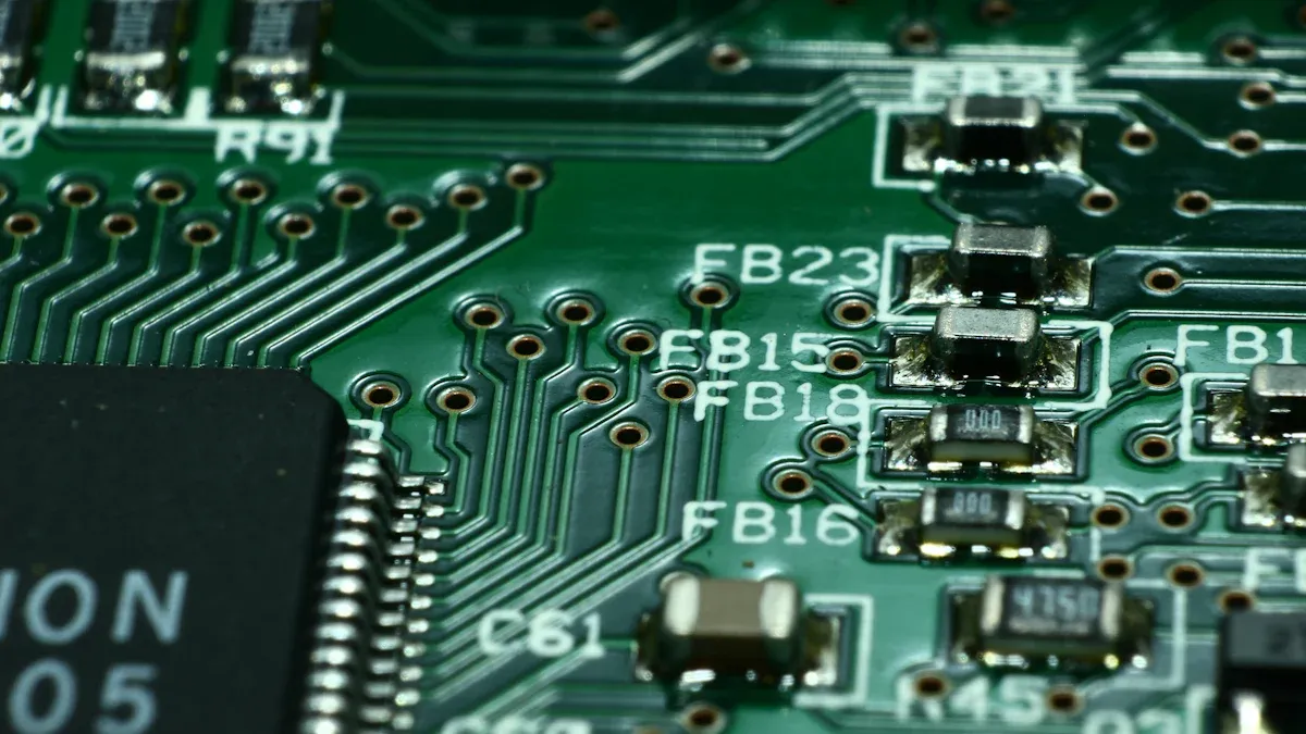
You need to understand the meaning of schematic diagram before you start any pcb project. In pcb design, a schematic diagram is a two-dimensional drawing that shows how electronic components connect to each other. This diagram uses standardized symbols for parts like resistors, capacitors, and transistors. You see the logic of the circuit before you move to the layout phase of the printed circuit board. The schematic helps you visualize the flow of signals and power across the circuit board.
When you create a schematic, you include several key elements to make sure your design is accurate and easy to follow. Here is what you should check in every schematic diagram:
- Verify pin numbering and labels for each component and match them with the datasheet.
- Conduct a polarity check for all polarized components in the schematic.
- Check for overlapping labels and pin numbers to keep the diagram readable.
- Validate the alignment of base, collector, and emitter pins of transistors with the datasheet, schematic symbol, and footprint package.
- Confirm the accuracy of component values, reference designators, and physical locations.
- Ensure the presence of schematic symbol descriptions, such as manufacturer part number, vendor name, and vendor part number.
- Check for the presence and accuracy of off-page connectors.
- Verify inter-sheet references for seamless connectivity.
- Conduct checks on decoupling capacitors for all ICs, ensuring proper ground pin separation based on signal type.
- Perform bill of materials checks, including package types, quantity, and part numbers.
Tip: Always double-check your schematic diagram before moving to the pcb layout. This step helps you avoid errors and saves time during assembly.
You use the schematic to guide the design of your printed circuit board. The diagram gives you a clear map of how each part works together. You rely on the schematic to communicate your ideas to other designers and technicians. The meaning of schematic diagram goes beyond just drawing lines and symbols. It represents the logic and function of your entire circuit board.
Schematic Diagram vs. Other Diagrams
You might wonder how a schematic diagram differs from other diagrams used in pcb design. You often see wiring diagrams and layout diagrams, but each serves a unique purpose.
Here is a comparison to help you understand the differences:
| Feature | Schematic Diagrams | Wiring Diagrams |
|---|---|---|
| Purpose | Focus on logical arrangement and functioning of components | Provide a pictorial view of components’ physical locations |
| Representation | Uses symbols to represent components and connections | Shows components in their approximate physical locations |
| Use Case | Useful for troubleshooting and understanding circuit logic | Used for wiring installation in homes and industries |
You use schematic diagrams to understand the logic and function of the circuit. Wiring diagrams show you where each part sits on the circuit board or in a system. You need both types, but the schematic is essential for pcb design because it helps you plan and troubleshoot the circuit.
Layout diagrams also play a role in pcb design. These diagrams show the physical placement of components on the printed circuit board. However, schematic diagrams offer several advantages over layout diagrams:
| Feature | Description |
|---|---|
| Component symbols and reference designators | Schematics use symbols to represent components, making it easier to understand circuit functionality. |
| Net names and signal flow paths | They illustrate how signals flow through the circuit, clarifying the logical relationships. |
| Hierarchical blocks or subsystems | This allows for better organization of complex circuits, enhancing readability and design clarity. |
| Power and ground connections | Clearly defined connections ensure proper circuit functionality and power distribution. |
| Pin numbers and annotations | These provide additional information for assembly and troubleshooting, aiding in the design process. |
You see that schematic diagrams help you organize complex circuits and make your pcb design process smoother. You use the schematic to check signal flow, power distribution, and component relationships. The diagram gives you the information you need to build a reliable printed circuit board.
Note: You should always start with a schematic diagram before creating wiring or layout diagrams. This approach ensures your circuit board works as intended and reduces errors during assembly.
You now know the meaning of schematic diagram in pcb design. You use the schematic to plan, organize, and communicate every detail of your circuit board. This diagram is the foundation for successful pcb projects and helps you avoid mistakes in both design and assembly.
Standards and Symbols in Schematic Diagrams
Common PCB Symbols
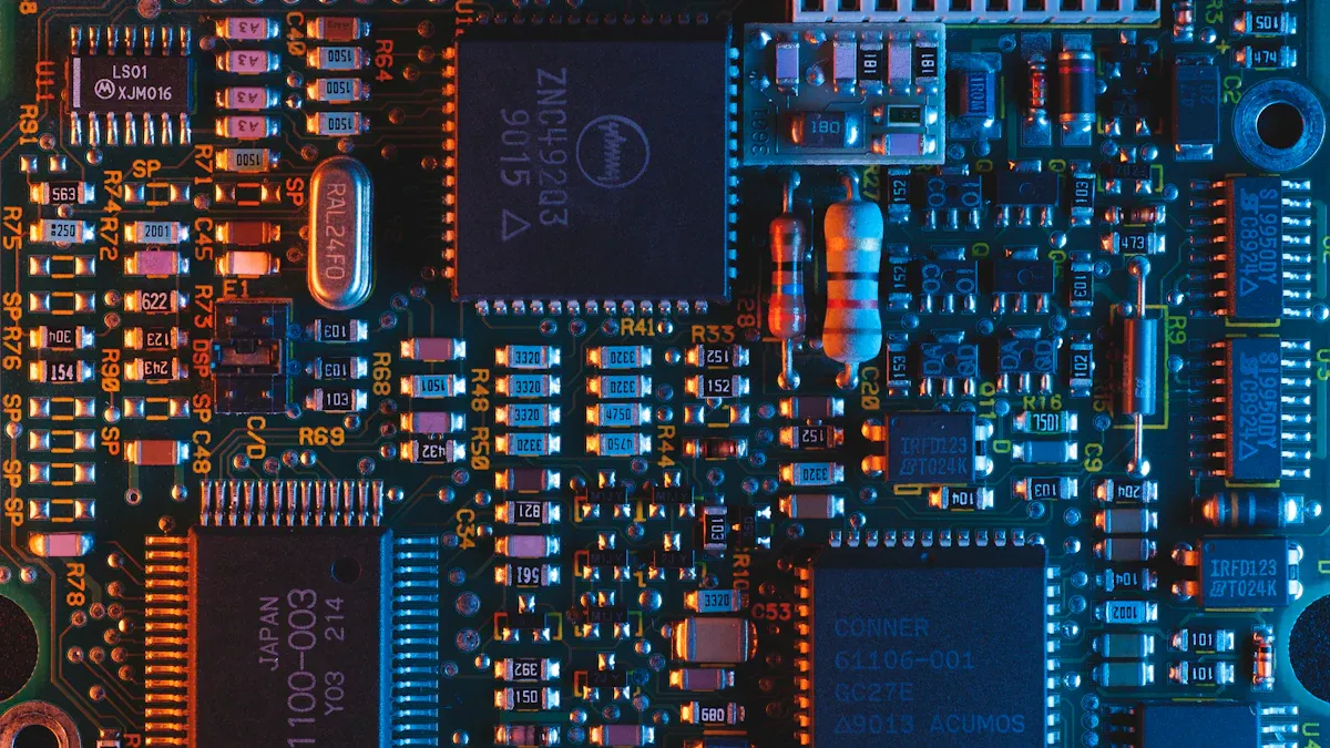
When you work with a schematic diagram, you rely on symbols to represent each part of the circuit. These symbols help you read and understand the schematic quickly. In pcb projects, you see these symbols in every schematic wiring diagram. Each symbol stands for a specific component or function. You use these symbols in cad tools to create your schematic design and to communicate with others.
Here is a table showing some of the most common symbols you will find in a pcb schematic diagram:
| Symbol Type | Description |
|---|---|
| AC | Represents Alternating Current, which changes direction over time. |
| DC | Represents Direct Current, which flows in only one direction. |
| Cell | Shows a single energy source with positive and negative ends. |
| Battery | Made of several cells connected together to provide more power. |
| Current Source | A circle with an arrow, showing the direction of current flow. |
| Voltage Source | A circle with a wave (AC) or plus/minus sign (DC) inside, showing the type of voltage. |
| Resistor | Limits the flow of current, with different symbols for types of resistors. |
| Capacitor | Stores electrical charge and filters signals, with unique symbols for each type. |
You use these symbols in every schematic wiring diagram you create in cad software. This makes your pcb design clear and easy to follow. When you share your schematic, others can understand your diagram without confusion.
Tip: Always double-check your schematic symbols in your cad tool before you finish your schematic design. This step helps you avoid mistakes in your pcb assembly.
Industry Standards for PCB Design
You need to follow industry standards when you create a schematic diagram for a pcb. These standards make sure your schematic wiring diagram is clear and accurate. Most cad programs for pcb use the same set of rules and symbols. This helps you work with other designers and technicians without confusion.
The most common standards for schematic diagrams in pcb design include:
- IEEE and IEC standards for schematic symbols and diagram layout.
- IPC-2221, which gives general requirements for pcb schematic design and layout.
- ANSI Y32.2, which covers graphic symbols for electrical and electronics diagrams.
You use cad and computer-aided design tools to follow these standards. These programs help you create a schematic diagram that meets industry rules. When you use cad for your schematic design, you make your pcb project easier to build and troubleshoot.
Note: Following standards in your schematic wiring diagram helps you avoid errors and makes your pcb more reliable.
You see that using cad and computer-aided design tools with the right standards and symbols is key to a successful pcb schematic. This approach helps you create a clear, accurate diagram that guides your pcb assembly from start to finish.
Reading and Creating Schematic Diagrams
How to Read a Schematic Diagram
When you start reading a pcb schematic, you need to look for the logical flow of the circuit. Begin by identifying the power sources and ground connections. Trace the signal paths from input to output. You should recognize the standardized symbols for electronic components and understand how they connect. Reading a pcb schematic requires you to pay attention to component labels and designators. These help you match each part to its place in the circuit design.
To interpret complex diagrams, you need several skills:
- Understand logical connections between components
- Know how to read component labeling and designators
- Organize schematics into functional sections
- Recognize standardized symbols for circuit elements
- Troubleshoot and draft accurate schematics
You can use examples of schematic diagrams to practice these skills. This will help you become more confident in reading and understanding any schematic diagram you encounter.
Best Practices for PCB Schematic Design
When creating a schematic diagram, you should follow best practices for drawing schematic diagrams. These practices help you avoid mistakes and make your design easy to read. A well-designed pcb schematic improves communication and reduces errors during assembly.
| Best Practice | Description |
|---|---|
| Move symbols and nets | Adjust symbols and nets for space and readability, avoiding overlap. |
| Create net and component classes | Set up classes early to help with layout constraints. |
| Include essential information | Add part numbers, product info, revision numbers, and company details. |
| Run design rule checks | Check for errors like missing connections during and before layout. |
| Maintain readability | Make sure the schematic is correct and legible for everyone. |
| Ensure logical flow | Arrange symbols and nets for clear logic, important for high-speed circuits. |
| Leave room for nets | Give enough space for nets, names, and pin numbers to stay clear. |
You should always check that your schematic matches the physical layout. This step helps you avoid confusion and supports custom pcb design projects.
Maintaining the correct pin order is crucial for ensuring that the schematic serves its purpose effectively. If the pins are not in their correct physical order, it can lead to mistakes and confusion when comparing the schematic with the actual PCB design.
Common Mistakes in PCB Assembly
You can avoid many common mistakes by following best practices and checking your schematic carefully. Some errors happen when you do not keep the schematic intuitive or do not match the pin order with the physical board. You should create schematics that resemble the physical layout of the pcb. Use a schematic where pins are in their original order to help with component placement and rotation. This approach makes the schematic useful for debugging and understanding circuit functionality.
When creating a schematic diagram, always double-check connections and component values. Missing or mislabeled parts can cause problems in the final circuit design. You should also make sure that all electronic components are included and clearly labeled. This attention to detail helps you build reliable circuits and supports successful pcb assembly.
You see that schematic diagrams are the starting point for every successful PCB design and assembly. These diagrams give you a clear visual map of circuit connections and guide each step in your project. When you focus on accuracy and clarity, you reduce mistakes and make your work easier to understand. Schematic diagrams help you follow standards and avoid costly errors.
To improve your skills, try these steps:
- Define your circuit and choose the right components.
- Add and label each part using your software’s library.
- Connect components with wires based on your circuit logic.
- Use error-checking tools to find and fix mistakes.
Remember, a strong schematic diagram leads to better results and helps you build reliable PCBs.
FAQ
What is the main purpose of a schematic diagram in PCB assembly?
You use a schematic diagram to show how each electronic part connects. This diagram helps you understand the circuit and guides you during assembly.
How do you read component symbols in a schematic diagram?
You look for standardized symbols in the diagram. Each symbol stands for a specific part, like a resistor or capacitor. You match symbols with the legend or reference table.
Why should you double-check your schematic before starting PCB design?
You catch errors early when you review your schematic. This step saves you time and prevents mistakes during the design and assembly process.
What tools help you create and check schematic diagrams?
You use CAD software to draw and review your schematic. These tools offer error-checking features and make your diagrams clear and accurate.
Can you use a schematic diagram for troubleshooting?
You can use the schematic to find faults in your circuit. The diagram helps you trace connections and locate problems quickly.


