Step-by-Step Guide to the BGA SMT Assembly Process
I approach every SMT PCB assembly process with a commitment to quality control and accuracy. In my experience with BGA SMT, I rely on data-driven methods to prevent defects and improve reliability.
- Decision tree classifiers help me evaluate and enhance quality control in SMT PCB assembly.
- SPI parametric data and package warpage analysis allow me to predict and avoid common defects.
- The interpretability of these models supports continuous improvement across every assembly process step.
Key Takeaways
- Start every BGA SMT assembly with thorough inspections of components and PCBs to catch defects early and ensure quality.
- Prepare boards and components carefully by baking to remove moisture and applying the right amount of flux for strong solder joints.
- Use high-quality stencils and control solder paste volume precisely to achieve consistent, reliable solder printing.
- Combine manual and automated inspections like SPI, AOI, and X-ray to detect defects at every stage and improve yields.
- Maintain precise alignment, temperature control during reflow, and thorough cleaning to protect solder joint integrity and long-term reliability.
Incoming Inspection
Component Check
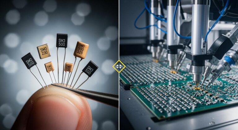
I always begin the BGA SMT assembly process with a thorough component check. This step sets the foundation for quality and reliability. I use both manual and automated methods to verify that every component meets strict standards before assembly. Automated Solder Paste Inspection (SPI) uses laser scanning and image processing to confirm solder paste volume, shape, and alignment. For the first assembled board, I perform a First Article Manual Inspection. This step verifies component placement and Bill of Materials (BOM) accuracy, creating a ‘golden’ reference board. Automated Optical Inspection (AOI) then compares production boards to this reference, detecting placement and solder defects. When I work with BGAs or complex packages, I rely on X-ray inspection and sometimes endoscopic inspection to check solder joint quality.
I tailor the incoming component inspection process based on component type, supplier history, and material sensitivity. This approach helps me catch issues early and control quality costs. I always keep in mind the industry benchmarks and acceptance criteria:
| Benchmark / Criterion | Description |
|---|---|
| Acceptable Quality Level (AQL) | Maximum defect rate accepted with 95% confidence; producer risk (α); 5% chance of rejecting good batches |
| Lot Tolerance Percent Defective (LTPD) | Defect rate at which 90% of batches are rejected; customer risk (β); 10% chance of accepting bad batches |
| Inspection Types | Full inspection (small quantity, high unit price), Sampling inspection (large quantity), Exemption (large quantity, low unit price, certified suppliers) |
| Inspection Items | Appearance, dimensional, characteristic, electrical, chemical, physical, environmental tests |
| Sampling Plans | Attribute data (counting defects), variable data (measurement-based), SPC software parameters include AQL, LTPD, producer and customer risk |
| IQC Role | Incoming Quality Control is critical for supplier evaluation and controlling quality cost |
PCB Inspection
I never skip PCB inspection, as it is essential for preventing downstream defects. I check each bare board for visual and dimensional accuracy. I follow IPC-6012 standards, which define qualification requirements for rigid PCBs. These standards cover material quality, workmanship, and reliability. I look for defects such as annular ring breakouts, misregistration, and solder mask issues. IPC-A-600 provides visual acceptance criteria, helping me judge whether a board meets the required quality level, such as Class 2 or Class 3. By referencing these standards, I ensure that every PCB meets electrical and mechanical performance expectations before moving forward with assembly. This attention to detail at the inspection stage helps me deliver reliable, high-performance assemblies every time.
SMT Preparation
Baking Process
I always start the SMT preparation by baking the printed circuit boards and moisture-sensitive components. Moisture can hide inside materials during storage or shipping. If I skip this step, trapped moisture may expand rapidly during reflow, causing delamination, popcorning, or microcracks. These issues often lead to defects in smt assembly and reduce long-term reliability. I set the baking temperature and duration based on the component’s moisture sensitivity level. For most chip mounting processes, I use a standard of 125°C for 8 to 24 hours. This step ensures that the boards and components remain dry and stable before mounting. I monitor the oven closely to avoid overheating, which could damage sensitive parts. By following this routine, I prevent moisture-related failures and improve the overall quality of the smt process.
Flux Application
Proper flux application plays a critical role in chip mounting and smt reliability. I select the flux type and amount based on the component and solder paste specifications. Too little flux can leave oxides on metal surfaces, while too much can cause excessive residue and require more solder paste. Both situations can compromise solder joint quality. I always aim for a balanced application to minimize voids and ensure strong electrical and mechanical connections.
Tip: I use automated dispensers for consistent flux coverage, especially for fine-pitch mounting and BGA packages.
The relationship between flux and solder joint reliability is clear. The table below summarizes key aspects:
| Aspect | Summary | Impact on Reliability |
|---|---|---|
| Flux Type and Amount | High-activity, correct quantity reduces voids in joints | Improves electrical, thermal, and mechanical performance |
| Void Formation Mechanism | Voids form from outgassing and oxide reduction; poor application increases voids | Higher resistance, thermal stress, and risk of joint failure |
| Void Location and Size | Small voids at pad boundaries are riskier than larger central voids | Boundary voids threaten mechanical integrity |
| Standards | IPC-A-610D sets acceptable void levels | Ensures voids do not compromise reliability |
| Flux Residues and Quantity | Excess flux leaves residues, may require more solder paste | Optimal amount balances void reduction and residue control |
I always check that my flux application meets IPC standards. This attention to detail helps me avoid common mounting problems and ensures that every smt assembly delivers reliable performance.
Solder Paste Printing
Stencil Printing
I always treat stencil printing as a critical step in the BGA SMT assembly process. The quality of the stencil directly affects the outcome of solder paste printing. I select stencils with precise apertures and high-quality materials to ensure consistent paste transfer. Nanocoated stencils have become my preferred choice because they reduce paste volume variation and improve print consistency. I monitor the process by checking the mean solder paste volumes and Cpk values. Stencil D, for example, consistently delivers the highest mean volumes and Cpk, which means it provides superior accuracy and reliability.
| Stencil Type | Mean Paste Volume | Cpk Value | Standard Deviation | Cp Value |
|---|---|---|---|---|
| Standard | Medium | 1.8 | Higher | 2.1 |
| Nanocoated | High | 2.9 | Lower | 3.2 |
| Stencil D | Highest | 3.1 | Lowest | 3.5 |
Tip: I always use statistical tests like ANOVA to compare stencil performance. This helps me select the best stencil for each project.
Paste Volume Control
Precise paste volume control is essential for reliable solder joints. I use advanced online learning models, such as Support Vector Regressor (SVR), to predict and adjust solder paste volume in real time. These models achieve R2 values of 92% for averages and 81% for standard deviations, which gives me confidence in their accuracy. By monitoring paste volume, I can quickly detect and correct any deviations during solder paste printing. This approach reduces defects and ensures every joint meets quality standards.
I always check the process capability index (Cp) for each print run. Cp values greater than 3 indicate excellent process consistency, especially when using nanostencils. I also pay close attention to the standard deviation, as lower values mean less variation and higher reliability.
- I recommend regular calibration of the printing equipment.
- I always verify paste volume after each batch to maintain high standards.
Solder paste printing remains one of the most important steps in BGA SMT assembly. My focus on stencil quality and volume control helps me deliver consistent, defect-free results.
Solder Paste Inspection
Manual SPI
I always start my solder paste inspection process with a manual check. This step gives me a direct look at the quality of the paste deposits before moving to automated systems. I use a magnifying glass or a low-power microscope to examine the solder paste on each pad. I look for issues like insufficient coverage, bridging, or misalignment. These problems can cause defects later in the assembly process.
I follow a simple checklist during manual SPI:
- Check for even paste distribution on all pads.
- Look for any smearing or bridging between pads.
- Confirm that the paste sits within the boundaries of each pad.
- Inspect for any missing or excess paste.
Tip: I always document any defects I find during manual inspection. This record helps me identify patterns and improve my printing process over time.
Manual SPI works best for small batches or prototype runs. It allows me to catch obvious errors quickly. However, I know that manual inspection has limits. Human eyes can miss subtle defects, especially on high-density boards.
Automated SPI
For larger production runs, I rely on automated Solder Paste Inspection (SPI) systems. These machines use 3D imaging and laser scanning to measure the height, area, and volume of each solder paste deposit. Automated SPI gives me precise, repeatable results that manual inspection cannot match.
Here is what I monitor with automated SPI:
| Parameter | Why I Check It |
|---|---|
| Paste Height | Ensures proper joint formation |
| Paste Volume | Prevents opens and shorts |
| Pad Alignment | Reduces placement errors |
| Area Coverage | Confirms full pad coverage |
Automated SPI alerts me to trends and process drifts. I can adjust my stencil printing parameters in real time. This proactive approach helps me maintain high yields and consistent quality.
Note: I always calibrate my SPI equipment regularly. Accurate measurements depend on well-maintained machines.
By combining manual and automated SPI, I ensure every board meets my strict quality standards before moving to the next step.
BGA SMT Placement
Pick-and-Place
I always treat the pick-and-place step as the heart of smt pcb assembly. My experience shows that automated component placement delivers the speed and accuracy needed for modern electronics. I rely on advanced pick-and-place machines to handle chip mounting, especially for bga smt packages. These machines use precision nozzles and feeders to pick each component and place it onto the prepared pads. I program the machine to follow exact coordinates, ensuring every chip lands in the right spot.
To reduce placement errors, I focus on several key areas:
- I calibrate and maintain my pick-and-place machines regularly.
- I select high-quality nozzles and feeders to prevent misalignment or dropping.
- I monitor placement accuracy with advanced vision systems.
- I optimize conveyor speed and secure PCB fixturing to minimize component movement.
- I program the machine carefully and monitor the process closely.
Tip: Regular calibration and vision system checks help me catch small shifts before they become big problems.
The benefits of these improvements are clear. I see up to a 50% reduction in rework rates when I detect defects early using AOI and ICT. Automation of high-volume tasks like pick-and-place cuts labor costs by as much as 40%. By using data analytics and statistical process control, I address tombstone effects, which account for about 15% of reworks. Machine calibration, vision systems, and quality nozzles minimize misalignment errors and reduce the need for rework. Automated placement with real-time feedback accelerates production and shortens time-to-market.
| Improvement Area | Method/Action | Benefit |
|---|---|---|
| Rework Rate Reduction | Early defect detection via AOI and ICT | Up to 50% reduction in rework rates |
| Labor Cost Reduction | Automation of high-volume tasks | Up to 40% reduction in labor costs |
| Defect Rate Reduction | Data analytics and SPC for tombstone effects | 15% of reworks addressed proactively |
| Placement Accuracy | Calibration, vision, nozzle/feeder quality, feedback | Minimizes misalignment errors and reduces rework |
| Time-to-Market | Automated placement with real-time feedback | Faster production throughput and delivery |
I always keep these statistics in mind when I set up my smt pcb assembly line. They guide my decisions and help me deliver consistent, high-quality chip mounting results.
Alignment
Precise alignment is critical in bga smt and smt pcb assembly. I use high-resolution vision systems to align each component before mounting. These systems capture images of the PCB and the component, then calculate the exact position for placement. I rely on several alignment error metrics to validate the precision of my process.
| Metric/Parameter | Description |
|---|---|
| Least-square circle fitting | Finds centers of holes and pads on PCB images for precise alignment |
| Alignment shift values | Quantifies positional deviations from multiple images |
| Concentricity evaluation | Measures how well pad and hole centers align, indicating placement accuracy |
| Annular ring requirement | Specifies pad-to-hole alignment tolerance (0.5 ± 0.1 mm) |
| Relative coordinates | ΔLi, ΔWi (pad to image center), Δxi, Δyi (hole to pad) quantify positional offsets |
| Local deviation inspection | Vision system inspects small deviations at specific PCB points using image processing |
I use least-square circle fitting to find the centers of holes and pads. This method gives me a reliable reference for alignment. I calculate alignment shift values from multiple images to spot any positional deviations. Concentricity evaluation tells me how well the pad and hole centers match up, which is crucial for bga smt. The annular ring requirement, set at 0.5 ± 0.1 mm, ensures that the pad-to-hole alignment stays within acceptable limits. I also track relative coordinates and inspect local deviations with my vision system.
Note: Small alignment errors can lead to open or short circuits, especially in dense chip mounting. I always double-check alignment before reflow.
By focusing on these metrics, I maintain tight control over the smt pcb assembly process. My attention to alignment ensures that every mounting step meets the highest standards for reliability and performance.
Pre-Reflow Inspection
Visual Check
Before I send any board through the reflow oven, I always perform a careful visual check. This step allows me to catch obvious placement errors, missing components, or misaligned parts. I use a magnifier and good lighting to inspect each board. My eyes focus on solder paste coverage, component orientation, and pad alignment. I know that human inspection can catch 80-90% of visible defects, but fatigue and distractions can lower accuracy over time. I often rotate inspectors or take short breaks to keep my attention sharp.
Tip: I keep a checklist handy during visual checks. This helps me stay consistent and avoid missing critical details.
Although visual inspection works well for small batches or prototypes, I recognize its limitations. Manual checks take more time and can miss subtle defects, especially on dense BGA layouts. I always document any issues I find, so I can trace problems back to their source and improve my process.
AOI
For high-volume production, I rely on Automated Optical Inspection (AOI) systems. These machines use cameras and advanced algorithms to scan every board quickly and accurately. AOI detects misplaced components, insufficient solder paste, and polarity errors with impressive consistency. In my experience, AOI achieves a defect detection rate of 95-99%, far surpassing manual inspection. The system never gets tired or distracted, so I trust it for critical quality control.
| Inspection Method | Defect Detection Rate | Notes |
|---|---|---|
| AOI | 95-99% | Consistent high accuracy, automated, not affected by fatigue |
| Human Visual Check | 80-90% | Accuracy can degrade due to fatigue, manual inspection |
AOI has transformed my workflow. I have seen defect escape rates drop by 85% after implementing AOI. My first-pass yield improved from 92% to 98%. I always review AOI reports to spot trends and make process adjustments. By combining visual checks and AOI, I ensure that every board meets the highest standards before reflow.
Reflow Soldering
Temperature Profile
I always treat the temperature profile as the backbone of successful reflow soldering in smt pcb assembly. Precise control over each thermal zone ensures that every solder joint forms correctly, especially for bga smt packages. I use a thermal profiler with an accuracy of ±0.5°C. This level of precision allows me to monitor even the smallest temperature fluctuations. My profiler supports up to 12 channels, and I can extend it to 24 or 36 channels for complex boards. I set the recording rate at 50 milliseconds per channel, which gives me real-time feedback during every run. The profiler covers a wide temperature range, from -200°C to 1300°C, so I can handle any smt process requirement.
| Parameter | Value/Range |
|---|---|
| Thermal profiler accuracy | ±0.5°C |
| Number of temperature channels | Up to 12 (extendable to 24 or 36) |
| Recording rate | 50 ms per channel |
| Temperature range | -200°C to 1300°C |
I divide the reflow oven into four main zones: preheating, soaking, reflow (peak), and cooling. Each zone demands careful attention. In the preheating zone, I set the ramp rate between 1 and 3°C per second. This step prevents thermal shock and allows the board to heat evenly. The soaking zone maintains a stable temperature, which activates the flux and removes oxides from the pads and leads. During the reflow zone, I target a peak temperature between 235°C and 250°C. This range ensures the solder paste melts completely and forms strong joints. The cooling zone follows, where I control the cooling rate between 2 and 4°C per second. Rapid cooling helps prevent the formation of large solder grains, which can weaken the joints.
| Reflow Zone | Temperature Control Parameter | Typical Value/Range |
|---|---|---|
| Preheating Zone | Temperature ramp rate | 1 to 3°C per second |
| Soaking Zone | Soaking temperature stability | Constant temperature |
| Reflow Zone (Peak) | Peak temperature | 235°C to 250°C |
| Cooling Zone | Cooling rate | 2 to 4°C per second |
Tip: I always use simulation modeling to fine-tune my thermal profiles. This approach helps me meet target specifications for every smt pcb assembly.
Process Control
I rely on statistical process control (SPC) to monitor every critical parameter during reflow soldering. I track peak temperature, soaking temperature, and preheating slope using control charts. This method allows me to detect any variability and maintain process consistency. I also use artificial intelligence tools to predict optimal heating parameters. These tools help me achieve uniform temperature distribution across the entire board, which is essential for high solderability and reliability.
Precise temperature control is not just a technical requirement—it is the key to avoiding defects in smt pcb assembly. If I allow the temperature to fluctuate outside the set limits, I risk introducing defects such as cold joints, voids, or component warpage. I have seen that even a small deviation can lead to costly rework or field failures.
The impact of reflow soldering on BGA solder joint integrity cannot be overstated. I have observed that aging at elevated temperatures, especially above 150°C, significantly reduces the shear strength and reliability of solder joints. For example, SAC105 solder reliability drops to nearly half after six months at 125°C. Thermal cycling with longer high-temperature dwell times or larger temperature ranges increases cyclic fatigue damage, which reduces solder joint durability. The package type and solder alloy also play a role. Plastic BGA packages show better fatigue life than chip array BGAs because they experience lower stress levels. I have learned that faster ramp rates during thermal cycling or thermal shock cause higher accumulated strain energy density. This leads to more severe solder joint damage than slower ramp rates.
Experimental tests on BGA208 assemblies using SAC305 and Sn37Pb solder alloys have shown that higher solidification temperatures lead to failures at corner joints due to warpage stresses. Lower solidification temperatures cause failures under die edges because of shear stresses. Finite element analysis confirms that SAC305 solder joints experience higher residual and maximum stresses at corner joints. These findings highlight the importance of carefully controlling reflow soldering parameters, especially solidification temperature, to protect BGA solder joint integrity.
Note: I always validate my reflow profiles with both SPC data and real-world failure analysis. This practice helps me deliver smt pcb assemblies that meet the highest standards for reliability and performance.
Post-Reflow Inspection
AOI
After reflow soldering, I always begin my inspection process with Automated Optical Inspection (AOI). This step allows me to catch surface-level defects quickly and efficiently. I rely on AOI to identify missing components, incorrect placements, and solder bridges. The system scans each board with high-resolution cameras and advanced algorithms. I have seen how AOI transforms defect detection rates. For example, one contract manufacturer reduced post-reflow defect parts per million (DPPM) from over 30 to below 10 within weeks by introducing pre-reflow AOI and using short feedback loops for root-cause analysis. In my own work, I have observed similar improvements. Early detection and process optimization lead to fewer defects and higher yields.
AOI not only improves quality but also saves money. Lowering DPPM from 36 to 8 can save tens of thousands of dollars annually in high-volume production. I always review AOI reports to spot trends and adjust my process. This approach helps me maintain consistent quality and reduce repair costs.
Tip: I recommend combining AOI with other inspection methods for the most comprehensive results.
X-ray
I never rely solely on AOI for post-reflow inspection, especially when working with BGA packages. X-ray inspection, or Automated X-ray Inspection (AXI), allows me to see inside solder joints and detect hidden defects. I use X-ray to find voids, cracks, and poor solder joint formation that AOI cannot reveal. This method gives me confidence that every connection meets reliability standards.
Here is how combining AOI and X-ray benefits my process:
- AOI detects visible defects like missing parts and solder bridges.
- X-ray uncovers internal issues such as voids and cracks.
- Using both methods reduces post-reflow DPPM from typical industry levels of 100–300 down to 8–10.
- Comprehensive inspection leads to higher yields and lower rework costs.
- Product reliability improves, and customer returns decrease.
I always integrate both AOI and X-ray into my post-reflow inspection routine. This strategy ensures that I deliver defect-free assemblies and maintain a reputation for quality.
Cleaning
Flux Residue Removal
I always treat flux residue removal as a critical step in the BGA SMT assembly process. Flux residues can cause electrical leakage, corrosion, and even dendritic growth if left on the board. I use both manual and automated cleaning methods, depending on the assembly volume and board complexity. For small batches or prototypes, I prefer manual cleaning with lint-free wipes and high-purity isopropyl alcohol. This method allows me to target specific areas and inspect the results closely.
For high-volume production, I rely on automated cleaning systems. These machines use deionized water, specialized solvents, and ultrasonic agitation to remove residues from every corner of the PCB, including under BGA packages. I always verify the effectiveness of cleaning by inspecting the boards under UV light. This step helps me spot any remaining flux that could compromise reliability.
Tip: I recommend checking the compatibility of cleaning agents with PCB materials and components before starting the process.
Reliability
Cleanliness directly impacts the long-term reliability of every assembly I produce. Residual flux can lead to intermittent failures, corrosion, and reduced insulation resistance. I have seen how even small amounts of residue can cause field failures months after deployment. To prevent these issues, I follow industry standards like IPC-5704 and IPC-A-610 for cleanliness requirements.
I use ionic contamination testers to measure the cleanliness level of each board. These testers provide quantitative data, helping me ensure that every assembly meets strict reliability standards. I also document my cleaning process and test results for traceability.
| Cleaning Method | Best Use Case | Reliability Impact |
|---|---|---|
| Manual (Alcohol) | Prototypes, small runs | High if done thoroughly |
| Automated (Aqueous) | High-volume, complex | Consistent, repeatable |
By prioritizing thorough cleaning, I protect my assemblies from latent defects and deliver products that stand the test of time.
SMT Testing
In-Circuit Test
I always start my testing process with the in-circuit test. This method checks each component and connection on the assembled board. I use a bed-of-nails fixture that presses test probes onto specific points on the PCB. The fixture connects to a tester that measures resistance, capacitance, and voltage at each node. I can quickly find open circuits, shorts, and incorrect component values. This step helps me catch assembly errors before the board moves forward.
I rely on in-circuit testing because it gives me fast feedback. I can test hundreds of points in seconds. If I find a problem, I can trace it back to the exact location. This approach saves time and reduces rework costs. I always keep my test fixtures clean and calibrated to ensure accurate results.
Tip: I recommend updating test programs whenever you change the smt layout or component list. This practice prevents false failures and missed defects.
Functional Test
After in-circuit testing, I move to the functional test. This step checks if the assembled board works as intended. I power up the board and run it through real-world scenarios. I use custom test jigs and software to simulate operating conditions. For example, I might send signals through input pins and measure the output response.
Functional testing helps me verify that the smt assembly meets design requirements. I look for issues like firmware errors, timing problems, or signal integrity faults. If the board passes this test, I know it is ready for deployment. I document all results and keep detailed records for quality assurance.
| Test Type | What It Checks | When I Use It |
|---|---|---|
| In-Circuit Test | Component placement, solder joints, shorts, opens | After smt assembly |
| Functional Test | Board operation, firmware, signal response | Before shipment |
I always combine both tests to ensure every smt board I produce is reliable and ready for the field.
Depanelization
PCB Separation
I always treat depanelization as a critical step in the BGA SMT assembly process. After completing all assembly and testing, I need to separate individual PCBs from the larger manufacturing panel. This step demands precision and care. If I rush or use the wrong method, I risk damaging delicate solder joints or introducing microcracks, especially around BGA packages.
In my experience, I choose the depanelization method based on the board design and production volume. Here are the main techniques I use:
- Manual Breaking: I use this for simple boards with pre-scored V-grooves. I apply even pressure along the score line. This method works best for prototypes or small batches.
- Depaneling Routers: For complex shapes or high-volume runs, I rely on CNC routers. These machines cut along precise paths, minimizing mechanical stress. I always check the router bit condition before each job.
- Laser Depaneling: When I work with sensitive or high-density boards, I prefer laser depaneling. The laser creates clean edges without physical contact. This method reduces the risk of stress fractures near BGA joints.
- Punching: For very high-volume production, I sometimes use punching dies. This method offers speed but requires careful die maintenance to avoid burrs or cracks.
Tip: I always support the PCB during separation to prevent flexing. I use fixtures or soft pads to absorb shock and protect components.
I inspect each board after depanelization. I look for edge chipping, solder joint cracks, or lifted pads. If I find any defects, I trace them back to the depanelization process and adjust my method. Clean separation ensures that every board maintains its electrical and mechanical integrity.
| Depanelization Method | Best Use Case | Risk Level |
|---|---|---|
| Manual Breaking | Prototypes, simple | Moderate |
| CNC Routing | Complex, high-volume | Low |
| Laser Depaneling | Sensitive, high-density | Very Low |
| Punching | Mass production | Moderate-High |
By focusing on careful PCB separation, I protect the quality of my assemblies and deliver reliable products to my customers.
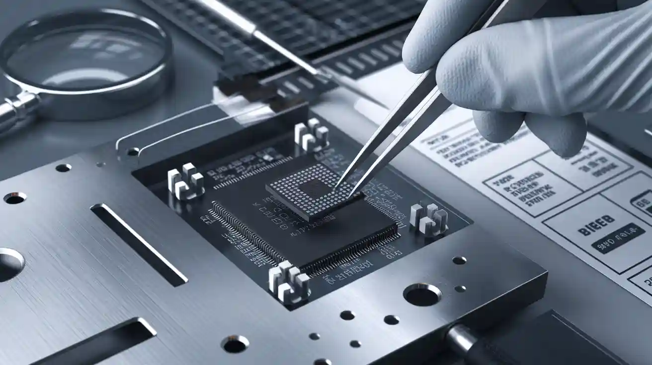
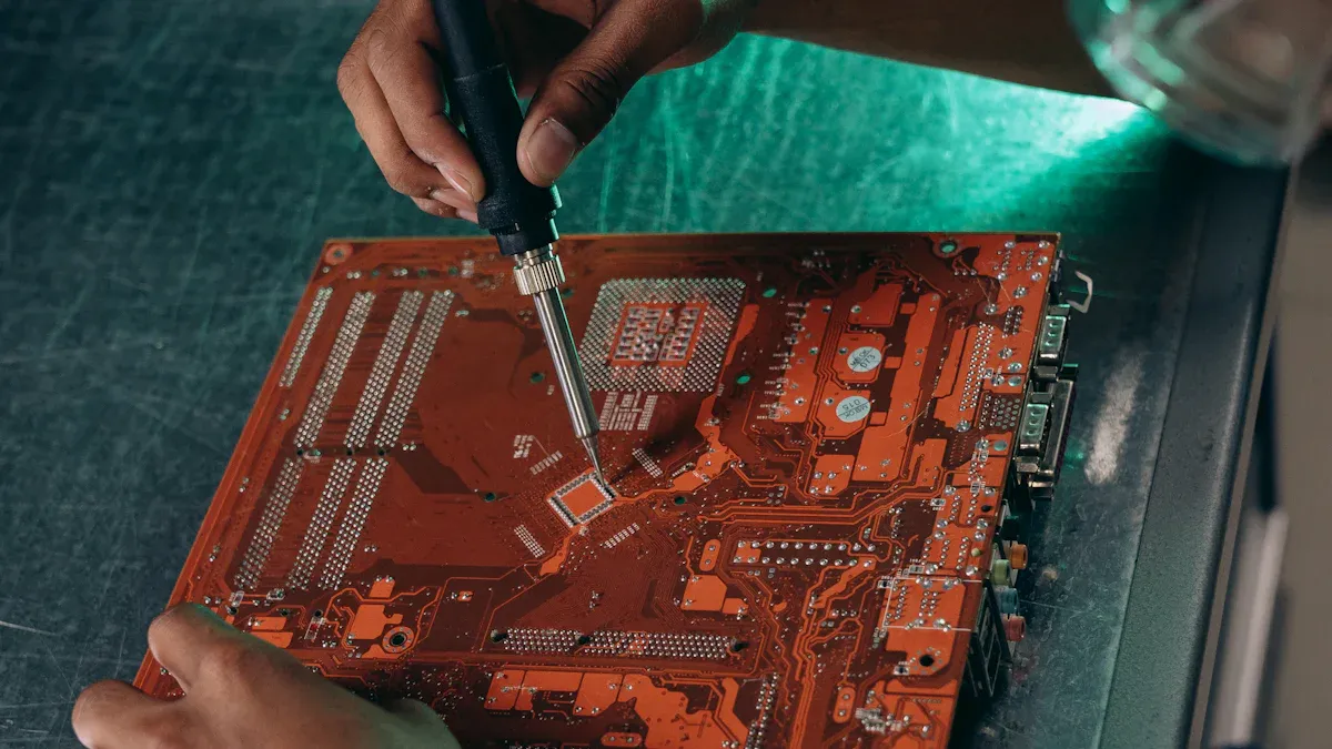
BGA Reballing
Removal
When I encounter a BGA component with faulty solder joints or need to replace it, I start with careful removal. I use a precision hot air rework station for this process. I set the temperature based on the solder alloy, usually between 220°C and 250°C for lead-free solder. I always shield nearby components with heat-resistant tape to prevent accidental damage.
I position the nozzle directly above the BGA package. I apply even heat until the solder balls melt. I gently lift the BGA using vacuum tweezers. I avoid twisting or prying, which can damage pads or traces. After removal, I inspect the PCB pads under a microscope. I look for lifted pads, solder mask damage, or leftover solder. If I find any issues, I repair them before moving forward.
Tip: I always let the board cool naturally after removal. Rapid cooling can stress the PCB and cause microcracks.
Reballing Steps
I follow a structured process to reball a BGA component. This ensures reliable connections and extends the life of the assembly. Here is my typical workflow:
- Clean the BGA: I remove old solder using solder wick and flux. I clean the surface with isopropyl alcohol and a lint-free wipe.
- Apply Flux: I spread a thin, even layer of flux on the BGA pads. This step improves solder wetting and ball adhesion.
- Place Solder Balls: I align a reballing stencil over the BGA. I place new solder balls into the stencil apertures, making sure each pad receives one ball.
- Reflow the Balls: I heat the assembly in a reflow oven or use a hot air tool. The solder balls melt and bond to the pads.
- Inspect and Clean: I check the new solder balls for uniformity and alignment. I clean off any flux residue.
| Step | Purpose | My Key Checkpoint |
|---|---|---|
| Clean the BGA | Remove old solder, debris | No residue or oxidation |
| Apply Flux | Promote solder adhesion | Even, thin coverage |
| Place Solder Balls | Prepare for reflow | All pads have one ball |
| Reflow the Balls | Form new solder joints | Balls fully melted, shiny |
| Inspect and Clean | Ensure quality, reliability | No bridges, no residue |
I always document each reballing job. This record helps me track quality and spot recurring issues. By following these steps, I restore BGA components to like-new condition and maintain high assembly standards.
I believe that a successful BGA SMT assembly process starts with careful inspection, continues with precise preparation, and ends with thorough testing. I always follow each step in the assembly process to ensure high reliability and performance. Attention to detail at every stage of the assembly process leads to fewer defects and better yields.
By following these best practices, I consistently deliver assemblies that meet the highest industry standards.
FAQ
What is the most common cause of BGA solder joint failure?
I often see moisture trapped in components or PCBs as the main cause. This moisture expands during reflow and creates microcracks or voids. Careful baking and moisture control prevent most failures.
How do I choose the right stencil for BGA SMT assembly?
I select stencils based on aperture size, thickness, and coating. Nanocoated stencils give me better paste release and consistency. I always check Cpk values and run statistical tests before finalizing my choice.
Can I skip X-ray inspection for small BGA assemblies?
I never skip X-ray inspection, even for small runs. X-ray reveals hidden defects like voids or cold joints that AOI cannot detect. This step ensures every assembly meets my reliability standards.
How do I prevent tombstoning during SMT assembly?
I balance solder paste volume, optimize reflow profiles, and calibrate my pick-and-place machine. I also monitor pad design and component placement. These steps help me reduce tombstoning and improve yields.
What cleaning method works best for removing flux under BGAs?
I use automated aqueous cleaning with ultrasonic agitation for BGAs. This method reaches under the package and removes residues. I always verify cleanliness with ionic contamination testing.