Step-by-Step Guide to PCB Etching for Beginners
PCB etching is a critical step in crafting custom printed circuit boards by removing unwanted copper to reveal your circuit design. This process allows you to create precise and functional layouts tailored to your electronics projects. Beginners find this technique approachable because it only requires basic tools like etching solutions and resist materials. Modern advancements, such as affordable laser cutters and detailed beginner guides, have further simplified the process. By mastering PCB etching, you can save costs, customize designs, and gain hands-on experience in electronics manufacturing.
Key Takeaways
- Collect basic tools like design software, a printer, and etching liquids.
- Stay safe by wearing gloves and working in fresh air.
- Clean your PCB well to remove dirt and rust.
- Watch the etching process carefully to avoid mistakes or damage.
- Try new designs and methods to improve and personalize your projects.
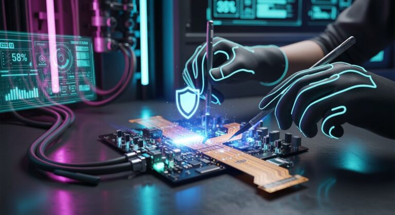
Tools, Materials, and Safety for PCB Etching
Essential Tools for the PCB Etching Process
To achieve precise results in the pcb etching process, you need the right tools. These tools help you design, transfer, and etch your circuit patterns effectively. Here’s a list of essential tools:
- Design Tools: Use CAD software to create and layout your circuit design. Tools like Altium Designer offer integrated environments for schematic capture and PCB layout.
- Transfer Tools: A laser printer or carbon-based toner photocopier is necessary for printing your design onto transfer paper. A laminator ensures proper adhesion of the design to the copper plate.
- Etching Tools: A glass dish or disposable plastic container (at least 6 inches square) is ideal for holding the etching solution. You’ll also need a brass brush for cleaning and scouring pads for surface preparation.
- Finishing Tools: A jeweler’s saw or metal shear helps trim the PCB to size. Sandpaper and a black permanent marker are useful for touch-ups.
These tools streamline the pcb manufacturing process, ensuring accuracy and efficiency.
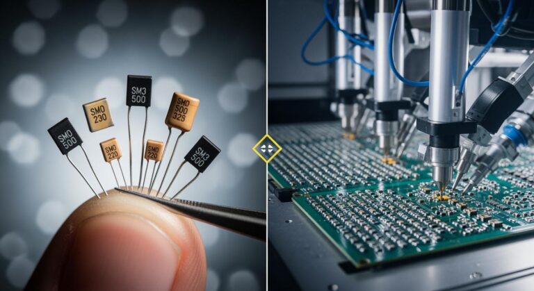
Materials Needed for PCB Etching
The materials you use directly impact the quality of your pcb. For top-notch pcb etching services, gather the following:
- Etching Solution: Ferric chloride is a popular choice for removing unwanted copper.
- Copper-Clad Board: Choose brass, copper, or nickel in 18, 20, or 22 gauge for etching.
- Resist Materials: PnP paper, nail polish, or contact paper can act as resist layers to protect areas of the board from the etching solution.
- Cleaning Supplies: Alcohol, baking soda, and water are essential for cleaning and neutralizing chemicals.
- Protective Gear: Nitrile gloves, safety glasses, and an apron protect you from harmful chemicals.
Using high-quality materials ensures durability and precision in your pcb fabrication process.
Safety Precautions for PCB Etching
Safety is paramount when working with chemicals during pcb etching. Follow these precautions to protect yourself and your workspace:
- Work in a Ventilated Area: Use a fan extraction hood to minimize exposure to fumes.
- Wear Protective Gear: Always wear nitrile gloves, goggles, and an apron to shield your skin and eyes.
- Handle Chemicals Responsibly: Store etching solutions securely and keep baking soda or diluted borax nearby to neutralize spills.
- Use Non-Metallic Containers: Avoid metal containers, as they can react with the etching solution.
- Dispose of Chemicals Properly: Follow local regulations for disposing of spent etching solutions to minimize environmental impact.
Adhering to these guidelines ensures a safe and efficient pcb manufacturing process, allowing you to focus on creating high-quality designs for your electronics projects.
Preparing Your PCB for the Etching Process
Cleaning and Prepping the PCB Surface
Before starting the etching process, you must ensure the PCB surface is clean and free of contaminants. Dust, grease, or oxidation can interfere with the adhesion of the resist layer and compromise the quality of your circuit. Follow these steps to prepare the surface effectively:
- Remove Oxidation: Use a fine scouring pad or brass brush to gently scrub the copper-clad board. This removes oxidation and creates a slightly rough surface for better resist adhesion.
- Clean the Surface: Wash the board with isopropyl alcohol to eliminate oils and debris. Avoid touching the copper surface with bare hands after cleaning.
- Dry Thoroughly: Use a lint-free cloth to dry the board completely. Any moisture left on the surface can affect the resist application.
A well-prepped PCB ensures that the copper traces remain intact during the etching process, leading to a precise and functional circuit.
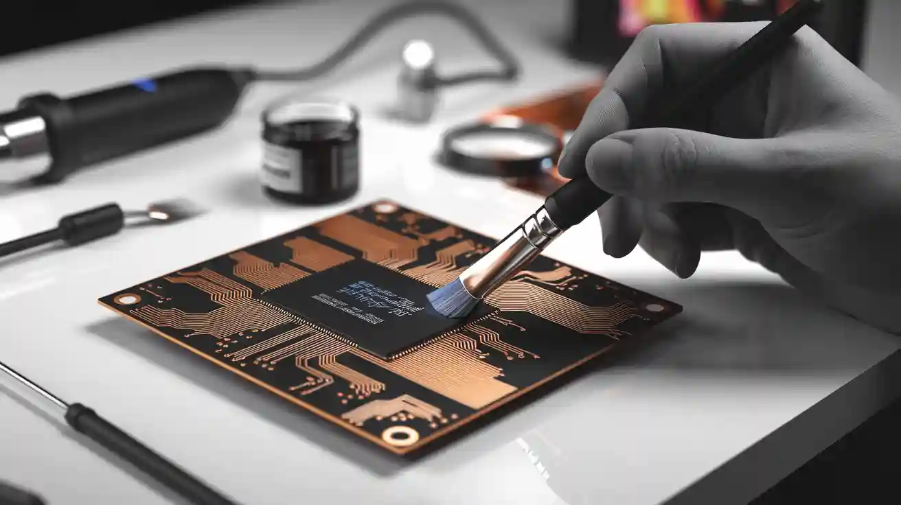
Applying the Resist Layer to the PCB
The resist layer protects the copper traces you want to keep while exposing unwanted areas to the etching solution. Several methods are available for applying the resist layer, each suited to different needs:
- Dry Film: This method provides uniform thickness and is ideal for intricate designs. It involves laminating a photosensitive film onto the PCB.
- Liquid Photoimageable (LPI): Known for its excellent resolution, this method uses a liquid polymer that hardens under UV light.
- Epoxy-Based Resists: These offer high chemical resistance and are suitable for harsh environments.
For beginners, using PnP (Press-n-Peel) paper or a permanent marker is a simpler alternative. These materials allow you to manually mask the copper traces, ensuring they remain protected during etching. Regardless of the method, ensure the resist layer adheres firmly to the board to prevent etching solution leaks.
Designing and Transferring the Circuit Pattern
Your circuit design determines the functionality of the PCB. Start by creating the design using CAD software, such as KiCad or Eagle. Once finalized, transfer the design onto the PCB:
- Print the Design: Use a laser printer to print the circuit pattern onto transfer paper. Ensure the design is mirrored so it aligns correctly on the board.
- Align the Design: Place the printed design face-down on the copper surface. Use tape to secure it in place.
- Transfer the Pattern: Apply heat using a laminator or iron to transfer the toner onto the PCB. The toner acts as a resist, protecting the copper traces during etching.
- Inspect the Transfer: Check for gaps or imperfections in the transferred pattern. Use a black permanent marker to touch up any areas where the toner did not adhere properly.
A precise transfer ensures that the copper traces match your circuit design, minimizing errors during the etching process.
Step-by-Step Guide to the PCB Etching Process
Setting Up the Etching Solution
The etching solution is the heart of the PCB etching process. It removes unwanted copper from the board, leaving behind the desired circuit traces. To set up the solution, follow these steps:
- Choose the Right Etchant: Ferric chloride is a popular choice due to its effectiveness and availability. Alternatively, a mixture of vinegar and hydrogen peroxide can serve as a safer, eco-friendly option.
- Prepare the Solution: Mix the etchant according to the manufacturer’s instructions. For ferric chloride, dilute the solution with water in a non-metallic container. If using vinegar and peroxide, combine them in a 2:1 ratio.
- Heat the Solution (Optional): Slightly warming the solution (to around 40°C) can speed up the etching process. Use a water bath to heat the container indirectly, ensuring even temperature distribution.
Tip: Always use a glass or plastic container to avoid chemical reactions with the etchant. Label the container clearly to prevent accidental misuse.
Properly setting up the etching solution ensures consistent results and minimizes the risk of errors during the process.
Immersing the PCB in the Etching Solution
Once the solution is ready, you can begin the etching process by immersing the PCB. This step requires precision and patience to achieve clean, well-defined copper traces. Here’s how to proceed:
- Submerge the PCB: Place the PCB into the solution with the copper side facing up. Ensure the board is fully submerged for uniform etching.
- Agitate the Solution: Gently stir or rock the container to keep the solution moving. This prevents stagnant areas and ensures even exposure to the etchant.
- Monitor the Time: The immersion time depends on the type of etchant and the method used. Refer to the table below for guidance:
Etching Solution Rubbing Method Time Immersion Method Time Ferric Chloride 3 minutes 10 minutes Vinegar and Peroxide 11 minutes 20 minutes
Note: Avoid over-etching, as it can damage the copper traces. Check the board periodically to assess progress.
By carefully immersing the PCB and monitoring the time, you can achieve precise results without compromising the integrity of the copper traces.
Monitoring and Controlling the Etching Process
Effective monitoring and control are essential for a successful PCB etching process. This ensures that the copper is removed evenly, leaving behind clean and accurate circuit patterns. Focus on these key aspects:
- Temperature Stability: Maintain a consistent temperature throughout the process. Fluctuations can affect the etching rate and lead to uneven results. Aim for a stability of ±1°C.
- Solution Concentration: Regularly check the concentration of the etchant. A deviation of more than ±5% can impact the etching quality.
- Etching Rate Consistency: Monitor the rate at which the copper dissolves. An inconsistent rate (beyond ±10%) may indicate issues with the solution or agitation.
- Spray Pressure Uniformity: If using a spray etching system, ensure the pressure is evenly distributed across the PCB.
The table below summarizes these critical control parameters:
| Critical Control Parameter | Specification |
|---|---|
| Temperature stability | ±1°C |
| Solution concentration | ±5% |
| Etching rate consistency | ±10% |
| Spray pressure uniformity | N/A |
To further enhance the process, consider these advanced techniques:
- Use closed-loop etching systems to reduce chemical consumption by up to 40%.
- Implement real-time monitoring tools to improve yield by 5-8%.
- Opt for advanced nozzle designs in spray systems to enhance uniformity by 15%.
Callout: Semi-additive processes are ideal for achieving ultra-fine features and precise thickness control, especially in high-density interconnect (HDI) applications.
By closely monitoring these parameters and adopting best practices, you can achieve consistent and high-quality results in your PCB etching process.
Removing Excess Copper from the PCB
Removing excess copper is a crucial step in the PCB etching process. It ensures that only the desired circuit traces remain intact, providing a clean and functional design. Follow these steps to effectively remove unwanted copper from your PCB:
- Inspect the PCB: Examine the board after etching to identify areas where excess copper remains. Pay close attention to edges and intricate patterns, as these areas are prone to incomplete etching.
- Neutralize the Etching Solution: Prepare a neutralizing bath using a mixture of baking soda and water. Submerge the PCB to halt the chemical reaction and prevent further copper removal.
- Clean the PCB Surface: Use a brass brush or fine scouring pad to gently scrub the surface. This removes residual copper particles and ensures the traces are well-defined.
- Re-Etch Problem Areas: If excess copper persists, reapply the etching solution to the affected areas. Use a small brush for precise application, minimizing the risk of over-etching.
Tip: Always rinse the PCB thoroughly after each step to remove chemical residues. This prevents contamination during subsequent processes.
Advanced Techniques for Copper Removal
Several advanced methods can enhance the efficiency of copper removal during PCB etching. These techniques are widely used in industrial applications and can be adapted for hobbyist projects:
- Ammoniacal Etching: This method preserves tin/lead solder while efficiently removing copper. It is ideal for close trace applications and offers a longer service life compared to acidic solutions.
- Cupric Chloride Etching: Known for its high efficiency, this solution works well for intricate designs. It also allows for easier regeneration, reducing waste.
- MECER Process: This innovative approach combines copper recovery with etchant regeneration. It is particularly useful for large-scale PCB production, offering both environmental and economic benefits.
These methods demonstrate the versatility of copper removal techniques, allowing you to choose the best option for your specific needs.
Common Challenges and Solutions
Removing excess copper can sometimes present challenges. Here are common issues and practical solutions:
- Incomplete Etching: If copper remains in unwanted areas, increase the agitation during the etching process. This ensures uniform exposure to the solution.
- Over-Etching: To avoid damaging the traces, monitor the etching time closely. Use a timer to maintain precision.
- Residual Copper Particles: After cleaning, inspect the PCB under a magnifying glass. Remove any remaining particles using a fine brush or compressed air.
By addressing these challenges proactively, you can achieve consistent and high-quality results in your PCB fabrication process.
Finishing and Testing the PCB
Stripping the Resist Layer
Stripping the resist layer is a critical step in the pcb etching process. This step involves removing the protective material that shielded the copper traces during etching. Proper resist removal ensures the board is ready for further processing and assembly.
To strip the resist layer effectively, use a chemical solution designed for this purpose. Submerge the pcb in the solution and gently agitate it to dissolve the resist. Monitor the process closely to avoid damaging the copper. After stripping, rinse the board thoroughly with water to remove any residue. Dry the pcb completely before proceeding to the next step.
Tip: Keep a log of the resist type, exposure level, and bath age. This helps maintain consistency and control during the stripping process.
Drilling Holes for Components
Drilling holes is essential for mounting components onto the pcb. Precision is key to ensuring the holes align perfectly with the circuit design and component leads. Use a drill press or CNC machine for accurate results.
Follow these guidelines for drilling:
- Match the drill diameter to the component lead width. This ensures a snug fit without damaging the copper traces.
- Maintain an aspect ratio of 10:1 for through-holes to enhance reliability.
- Inspect the drilled holes for uniformity and perpendicularity. Use tools like a coordinate measuring machine (CMM) or microscopy for quality assurance.
| Criteria | Details |
|---|---|
| Drill Diameter | Match drill sizes to component lead widths, maintain adequate annular ring distances. |
| Minimize Aspect Ratio | Target 10:1 ratio for typical through holes to avoid reliability risks. |
| Quality Standards | Hole Diameter Tolerance: +/- 10μm, Perpendicularity Rating: >89°, Hole Circularity: uniformity. |
| Inspection Methods | CMM Validation, Microscopy, Cross-Sectioning for quality assurance. |
Note: Use sharp drill bits and proper feed rates to prevent burrs or damage to the copper surface.
Inspecting and Testing the PCB for Functionality
Testing ensures the pcb meets design specifications and functions as intended. Begin with a visual inspection to identify visible defects like scratches or incomplete traces. For more detailed analysis, use automated optical inspection (AOI) to detect assembly issues such as insufficient solder or cracked joints.
Functional testing simulates the pcb’s operation within its intended device. This step verifies that all components work correctly and the circuit performs as expected. Additionally, environmental stress testing evaluates the pcb’s durability under extreme conditions like thermal shock or vibration.
| Inspection Method | Description |
|---|---|
| Visual Inspection | Manual checks for visible defects |
| Automated Optical Inspection | Machine-based inspection for non-visible issues |
| X-ray Inspection | Examination of inner layers and solder joints |
| In-Circuit Testing (ICT) | Verification of component functionality |
| Functional Testing | Simulation of PCB operation within its intended device |
| Environmental Stress Testing | Testing under extreme conditions to ensure durability |
Callout: Testing protocols like failure analysis and statistical trend analysis help identify defects and improve future designs.
By following these steps, you can ensure your pcb is not only functional but also reliable for long-term use.
Tips and Troubleshooting for the PCB Etching Process
Avoiding Common PCB Etching Mistakes
Mistakes during the PCB etching process can lead to defective boards and wasted materials. By understanding common errors and how to prevent them, you can improve your results and reduce frustration. Here are some frequent issues and their solutions:
- Improper Surface Preparation: Failing to clean the copper-clad board thoroughly can cause poor adhesion of the resist layer. Always scrub the surface with a fine scouring pad and clean it with isopropyl alcohol before applying the resist.
- Inconsistent Resist Application: Uneven or incomplete resist layers can expose unintended areas to the etchant. Use high-quality resist materials and ensure even coverage across the board.
- Overexposure to Etching Solution: Leaving the PCB in the etchant for too long can result in over-etching, which damages the copper traces. Monitor the process closely and remove the board as soon as the unwanted copper dissolves.
- Poor Agitation: Stagnant etching solution can lead to uneven copper removal. Gently agitate the solution or rock the container to ensure uniform etching.
The table below summarizes key factors that contribute to etching mistakes and how to address them:
| Issue | Prevention Method |
|---|---|
| Improper Surface Cleaning | Use alcohol and scouring pads to remove oxidation and contaminants. |
| Uneven Resist Application | Apply resist evenly and inspect for gaps before proceeding. |
| Overexposure to Etchant | Monitor the process and follow recommended immersion times. |
| Poor Agitation | Stir or rock the solution gently to maintain uniform etching. |
Tip: Train yourself to inspect each step of the process carefully. This habit minimizes errors and ensures consistent results.
Fixing Over-Etching or Under-Etching Issues
Over-etching and under-etching are two of the most common challenges in PCB fabrication. Both can compromise the functionality of your board. Here’s how to identify and resolve these issues:
Over-Etching
Over-etching occurs when the etching solution removes more copper than intended, thinning or breaking the traces. To fix this:
- Inspect the Damage: Use a magnifying glass to identify affected areas. Look for broken or excessively thin traces.
- Repair the Traces: Apply conductive ink or solder to rebuild damaged traces. Ensure the repair is smooth and continuous.
- Adjust Future Processes: Reduce the immersion time or use a less aggressive etchant to prevent over-etching in future projects.
Under-Etching
Under-etching happens when the solution fails to remove all unwanted copper. To address this:
- Re-Etch the Board: Submerge the PCB back into the etching solution, focusing on the areas with excess copper. Use a small brush for precise application if needed.
- Check the Solution: Ensure the etchant is still effective. Replace it if the concentration has weakened.
- Improve Agitation: Stir the solution more frequently to enhance its effectiveness.
Note: Maintaining proper temperature and solution concentration can significantly reduce the likelihood of over-etching or under-etching.
Best Practices for Consistent PCB Etching Results
Consistency is key to producing high-quality PCBs. By following best practices, you can achieve reliable results every time. Here are some proven methods:
- Proper Agitation: Keep the etching solution in motion to ensure even copper removal. This prevents stagnation and improves efficiency.
- Temperature Control: Maintain a steady temperature throughout the process. Use a water bath to heat the solution evenly and avoid overheating.
- Accurate Masking and Alignment: Ensure the resist layer is applied precisely and aligns perfectly with your circuit design. This minimizes errors and enhances the board’s functionality.
- Regular Solution Maintenance: Monitor the concentration of your etching solution and replace it when necessary. A well-maintained solution delivers consistent results.
The table below highlights the benefits of these best practices:
| Best Practice | Benefits |
|---|---|
| Proper Agitation | – Ensures uniform etching across the board. |
| – Prevents stagnation of the etchant solution. | |
| – Improves overall efficiency of the etching process. | |
| Temperature Control | – Maintains a steady etching rate for consistent results. |
| – Prevents overetching and damage to the PCB. | |
| – Enhances safety by reducing risks associated with overheating. | |
| Accurate Masking and Alignment | – Prevents unwanted etching and ensures precision in circuit paths. |
| – Minimizes misalignment errors, leading to functional PCBs. | |
| – Ensures consistency in quality across all produced PCBs. |
Callout: Consistency in your process not only improves the quality of your PCBs but also reduces material waste and production costs.
By implementing these tips and troubleshooting techniques, you can master the PCB etching process and produce reliable, high-quality boards for your projects.
Mastering the pcb etching process involves several key steps, from preparing the board to finishing and testing. Each stage, such as applying the resist layer and carefully removing unwanted copper, requires precision to achieve functional circuit patterns. These control points, like maintaining plating thickness and line width, are essential for quality outcomes. As a beginner, you’ll find this process both accessible and rewarding. Experimenting with your designs not only enhances your skills but also allows you to create customized solutions for your projects. Start small, stay consistent, and enjoy the journey of crafting your own circuits.
FAQ
What is the best etching solution for beginners?
Ferric chloride is the most beginner-friendly etching solution. It is widely available, effective, and easy to handle. For a safer alternative, you can use a mixture of vinegar and hydrogen peroxide. Always follow safety precautions when working with any etchant.
Tip: Label your etching solution container to avoid accidental misuse.
How can I fix mistakes in my PCB design after etching?
You can repair minor mistakes using conductive ink or solder to reconnect broken traces. For larger errors, it’s better to start over with a new copper-clad board. Always double-check your design before transferring it to the PCB.
Can I reuse the etching solution?
Yes, you can reuse etching solutions like ferric chloride until they lose effectiveness. Monitor the solution’s performance, and replace it when etching takes significantly longer than usual. Dispose of spent solutions responsibly according to local regulations.
Note: Reusing the solution reduces waste and saves costs.
How do I ensure my resist layer adheres properly?
Clean the copper surface thoroughly with isopropyl alcohol and a scouring pad. Avoid touching the cleaned surface with bare hands. For better adhesion, apply the resist layer evenly and inspect for gaps before proceeding to etching.
Is PCB etching safe to do at home?
Yes, but you must follow strict safety guidelines. Work in a well-ventilated area, wear protective gear, and handle chemicals responsibly. Keep neutralizing agents like baking soda nearby to manage spills. Proper disposal of chemicals is also essential to protect the environment.
Emoji Reminder: 🧤 Always wear gloves and goggles for safety!