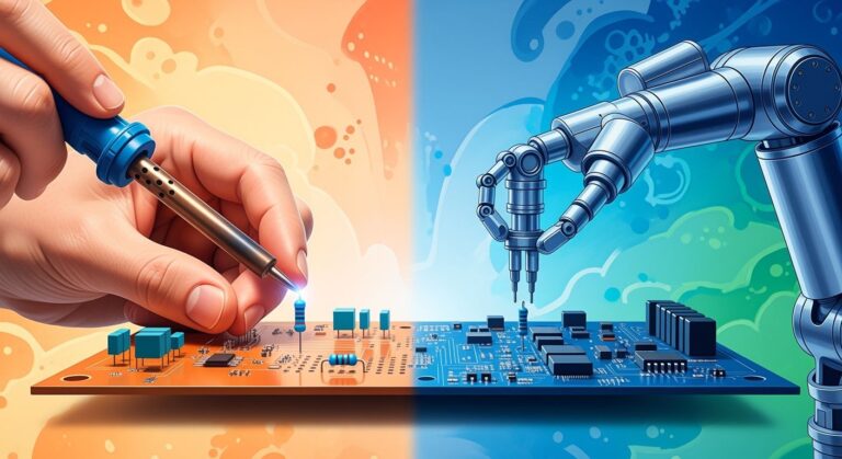
Top Tips for Optimizing PCB Assembly in 2025
In 2025, optimizing PCB assembly plays a pivotal role in transforming manufacturing efficiency and competitiveness. Tackling challenges like cost, speed, and reliability has become increasingly complex. For instance, PCB assembly planning is an NP-hard problem, requiring advanced strategies to streamline the process. Industry reports show that fully automated assembly lines can boost production capacity by up to 750%, cut defect rates to 0.02%, and reduce time-to-market by 65%. These advancements underscore the need for innovative solutions to meet evolving demands in assembly electronics manufacturing.
Key Takeaways
- Pick the right parts to save money and ensure reliability. Use common parts to make manufacturing easier and avoid supply problems.
- Use the same parts often to make work smoother. This lowers mistakes, improves quality checks, and cuts production costs.
- Plan for easy manufacturing from the start. This reduces waste and solves problems before they happen.
- Work with reliable PCB assembly companies. Their skills and quality checks make production better and prevent expensive mistakes.
- Use predictive maintenance to avoid breakdowns. This helps machines last longer and work more reliably.
Strategies for Cost-Effective PCB Assembly
Selecting Components for Cost and Reliability
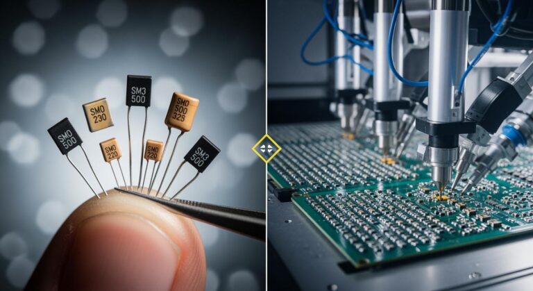
Choosing the right components is the cornerstone of cost-effective PCB assembly. I always emphasize the importance of planning during the design phase. This ensures that the selected components meet both performance and budgetary requirements. Engineers can optimize costs by using standard, widely available parts. These components not only simplify the manufacturing process but also reduce the risk of supply chain disruptions.
Additionally, collaborating with reliable suppliers is critical. High-quality components may seem expensive initially, but they minimize long-term costs by reducing failure rates and ensuring durability. Awareness of component lifecycles also helps avoid obsolescence, which can lead to costly redesigns. For example, a startup electronics company achieved a 30% cost reduction by optimizing component selection and leveraging flexible production setups, all without compromising quality.
Key strategies include:
- Simplifying the board design to reduce material costs.
- Using surface mount technology (SMT) to enhance design density and lower labor expenses.
- Minimizing the number of components to streamline assembly and testing.
These practices not only improve cost efficiency but also enhance the reliability of printed circuit boards.
Standardizing Components for Efficiency
Standardization is a game-changer in PCB assembly. By using uniform components, manufacturers can streamline operations and reduce production errors. This approach also simplifies quality checks, which is crucial for industries like healthcare and aerospace. For instance, standardization allows for economies of scale, reducing inventory complexity and lowering production costs.
| Benefit | Description |
|---|---|
| Enhanced Efficiency | Streamlines operations, reduces errors, and minimizes time for quality checks. |
| Improved Quality | Establishes clear benchmarks, reducing variability in critical applications. |
| Increased Competitiveness | Encourages innovation while ensuring compliance with industry norms. |
| Economies of Scale | Lowers costs by reducing inventory complexity and leveraging bulk purchasing. |
| Streamlined Operations | Simplifies supply chains and reduces the learning curve for new employees. |
Standardization also fosters continuous improvement by creating a framework for innovation. It ensures that the manufacturing process remains adaptable to new technologies while maintaining cost-effectiveness.
Designing for Manufacturability (DFM)
Design for manufacturability (DFM) is a vital strategy for optimizing the PCB assembly process. By integrating DFM principles early in the design phase, engineers can identify potential manufacturing constraints and address them proactively. This reduces production waste and improves overall efficiency.
| Principle | Impact on Production Waste |
|---|---|
| Material Conservation | Efficient use of materials reduces waste and costs. |
| Minimization of Waste | Optimized designs lead to less waste generation. |
For example, sustainable DFM practices align with circular economy goals by emphasizing resource optimization. This not only minimizes waste but also supports eco-friendly manufacturing. Incorporating DFM into the product lifecycle ensures that the final design is both cost-effective and reliable.
Key DFM practices include:
- Optimizing PCB layouts to reduce board size and material usage.
- Ensuring proper footprints for components to simplify assembly.
- Designing for test (DFT) to facilitate efficient testing and inspection.
These strategies enhance production efficiency while maintaining high-quality standards. A research institution, for instance, implemented advanced DFM techniques and rigorous testing procedures, achieving a 20% cost reduction compared to competitor quotes.
Partnering with Trusted PCB Assembly Providers
Partnering with trusted PCB assembly providers is essential for achieving consistent quality and reliability in manufacturing. I have seen firsthand how working with experienced providers can streamline production processes and reduce costly errors. These partnerships offer access to advanced technologies, skilled personnel, and rigorous quality assurance practices that are difficult to replicate in-house.
Why Trusted Providers Matter
Reliable PCB assembly providers bring expertise and infrastructure that enhance production efficiency. Their repeatability ensures consistent results across tests, while their versatility accommodates diverse PCB designs. Scalability is another advantage, as these providers can adapt to both small-scale prototypes and large-scale production runs.
| Performance Indicator | Description |
|---|---|
| Repeatability | Ensures consistent results across tests. |
| Versatility | Applicable to various PCB designs. |
| Scalability | Adaptable for both small and large production needs. |
These attributes make trusted providers invaluable for manufacturers aiming to meet tight deadlines without compromising quality.
Quality Assurance Practices
Trusted providers implement rigorous testing protocols to uncover latent defects. They simulate operating environments through methods like thermal cycling and vibration testing. This approach ensures that PCBs perform reliably under real-world conditions. Consistency across batches is another hallmark of quality providers. They maintain uniform standards across multiple production runs, which is critical for industries like automotive and aerospace. Certifications such as ISO 9001 and IPC-A-610 further demonstrate their commitment to quality assurance.
| Measure Type | Description |
|---|---|
| Testing Rigor | Simulates operating environments to uncover latent defects. |
| Consistency Across Batches | Ensures quality is maintained across multiple production runs. |
| Certifications | Compliance with standards like ISO 9001 and IPC-A-610. |
These practices not only enhance reliability but also build trust with clients who demand high-performance PCBs.
Quantifiable Benefits
Partnering with trusted providers delivers measurable benefits. Their defect detection rate identifies approximately 30% of PCB flaws, while high-fault coverage detects up to 90% of issues. Advanced testing methods allow simultaneous evaluation of multiple boards, significantly speeding up the process.
| Benefit Type | Quantitative Measure |
|---|---|
| Defect Detection Rate | Identifies approximately 30% of PCB flaws. |
| High-Fault Coverage | Detects up to 90% of issues. |
| Speed | Allows for simultaneous testing of multiple boards. |
These metrics highlight the tangible advantages of collaborating with experienced providers. I have observed how these benefits translate into reduced downtime, improved product reliability, and enhanced customer satisfaction.
Choosing the Right Partner
Selecting the right PCB assembly provider requires careful evaluation. I recommend assessing their track record, certifications, and technological capabilities. Providers with a proven history of delivering high-quality results and adhering to industry standards are ideal. Additionally, their ability to scale operations and adapt to evolving design requirements ensures long-term compatibility with your manufacturing goals.
By partnering with trusted providers, manufacturers can focus on innovation and growth while leaving the complexities of PCB assembly to experts. This collaboration fosters efficiency, reliability, and competitiveness in an increasingly demanding market.
Enhancing Speed in the PCB Assembly Process
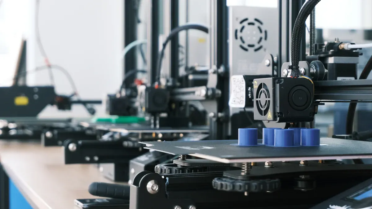
Leveraging Automation-Compatible Assembly Methods
Automation has revolutionized the PCB assembly process, enabling manufacturers to achieve unprecedented speed and efficiency. I have observed that adopting automation-compatible assembly methods is no longer optional—it is essential for staying competitive in modern manufacturing. By designing PCBs with automation in mind, manufacturers can streamline workflows and reduce manual intervention.
One effective approach is to prioritize surface mount technology (SMT) in the design phase. SMT allows components to be mounted directly onto the PCB surface, eliminating the need for through-hole drilling. This not only accelerates the assembly process but also enhances design density. For example, I’ve seen manufacturers reduce assembly times by up to 40% by transitioning from traditional methods to SMT-based designs.
Additionally, automated assembly systems thrive on consistency. Ensuring uniform component orientation and spacing simplifies the programming of automated pick-and-place machines, reducing setup times and errors. I always recommend collaborating with design teams to identify potential automation bottlenecks early in the process. This proactive approach minimizes disruptions and ensures a seamless transition to automated workflows.
Tip: Incorporate fiducial marks on PCBs to aid automated systems in accurate alignment and placement. This small design adjustment can significantly enhance assembly precision.
Optimizing Component Placement and Orientation
Efficient component placement and orientation are critical for speeding up the PCB assembly process. I’ve found that even minor adjustments in layout design can lead to significant improvements in assembly speed and quality.
To optimize placement, I recommend analyzing PCB designs for potential assembly issues. For instance, consistent component orientation facilitates automated assembly, reduces placement errors, and simplifies quality control inspections. Proper spacing between components also plays a vital role. It ensures that automated systems can operate without interference, minimizing the risk of errors.
Here’s a breakdown of key metrics that highlight the impact of optimized placement and orientation:
| Metric | Description |
|---|---|
| Consistent Component Orientation | Facilitates automated assembly, reduces placement errors, and simplifies quality control inspections. |
| Component Spacing | Optimizes the layout to enhance assembly speed and minimize errors. |
| Use of Fiducial Marks | Aids in accurate component placement and alignment during assembly. |
I always emphasize the importance of using fiducial marks. These visual alignment aids guide automated systems, ensuring precise placement even in high-speed operations. By addressing these factors during the design phase, manufacturers can achieve faster assembly times and higher yields.
Note: Regularly review and update design guidelines to align with the latest advancements in automated assembly technologies. This ensures that your processes remain efficient and competitive.
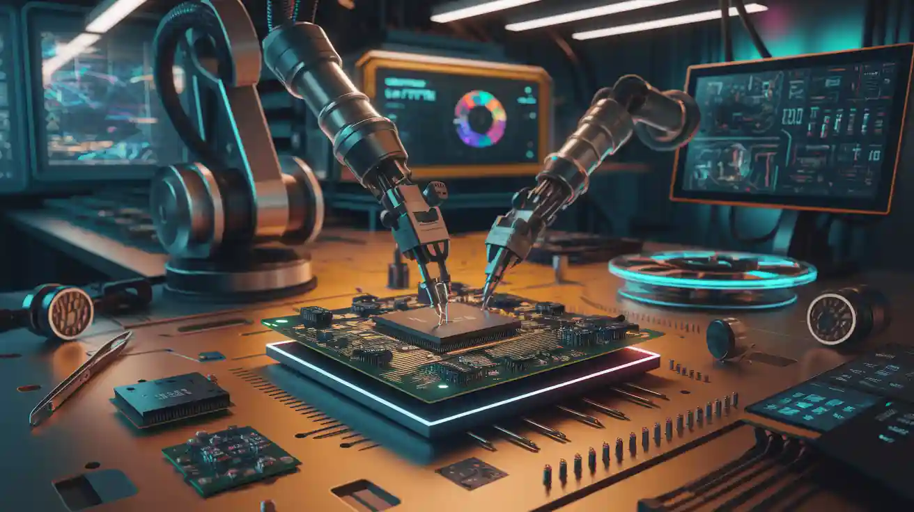
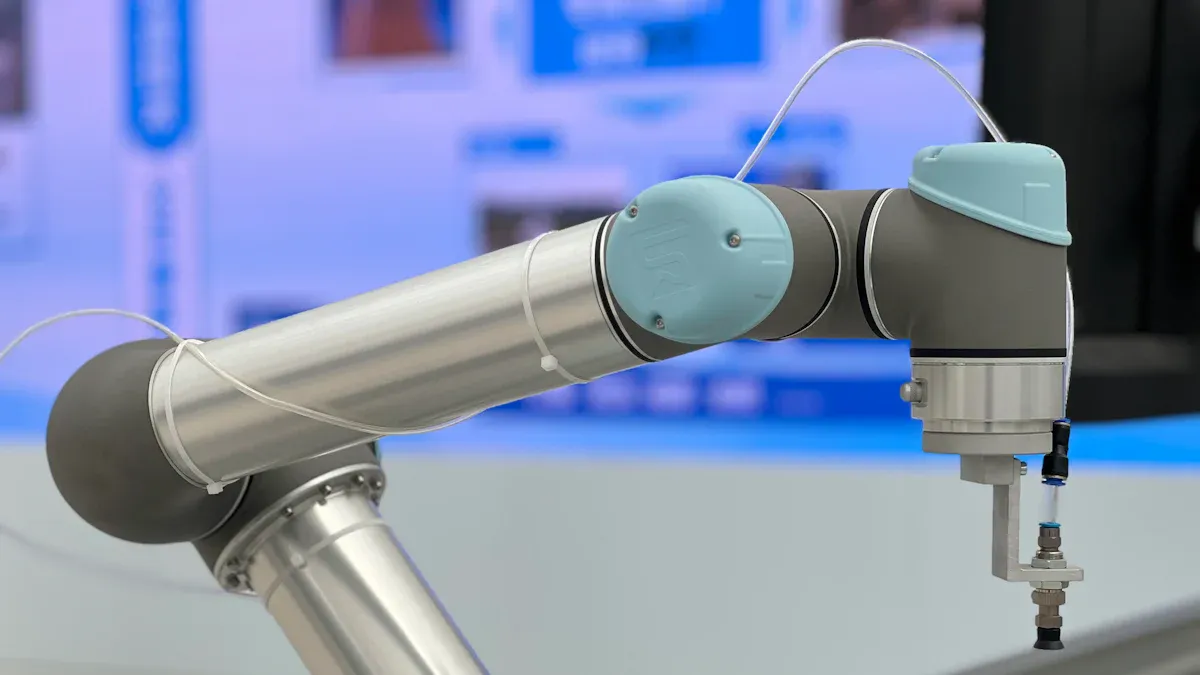
Implementing Advanced Pick-and-Place Machines
Advanced pick-and-place machines are the backbone of high-speed PCB assembly. These machines have evolved significantly, offering features that enhance both speed and accuracy. I’ve seen firsthand how investing in state-of-the-art equipment can transform the assembly process.
Modern pick-and-place machines, such as those equipped with MYCenter Analysis software, provide tools that help process engineers minimize component mispicks and rejects. This software enables real-time visualization of line performance, allowing manufacturers to identify bottlenecks and optimize equipment utilization. By leveraging data analysis, these machines ensure that every component is placed with precision, reducing rework and improving overall efficiency.
The benefits of automated pick-and-place systems extend beyond speed. They also enhance reliability by maintaining consistent performance across production runs. For example, I’ve worked with manufacturers who reported a 25% reduction in assembly errors after upgrading to advanced pick-and-place machines. These systems also support simultaneous placement of multiple components, further accelerating the assembly process.
Pro Tip: Regular maintenance and calibration of pick-and-place machines are essential for sustaining peak performance. Predictive maintenance tools can help identify potential issues before they disrupt production.
By integrating advanced pick-and-place machines into the assembly process, manufacturers can achieve faster turnaround times, higher accuracy, and improved product quality. This investment not only boosts operational efficiency but also strengthens competitiveness in a fast-paced market.
Reducing Downtime with Predictive Maintenance
Reducing downtime is critical in the PCB assembly process. I have observed that even minor disruptions can lead to significant delays and increased costs. Predictive maintenance has emerged as a powerful tool to address this challenge. By leveraging data-driven insights, manufacturers can anticipate equipment failures and schedule maintenance proactively, minimizing unplanned downtime.
One of the most effective ways to implement predictive maintenance is by using sensors and IoT-enabled devices. These technologies monitor equipment performance in real-time, identifying anomalies before they escalate into major issues. For example, vibration sensors can detect early signs of wear and tear in pick-and-place machines, allowing technicians to intervene before a breakdown occurs. This approach not only reduces downtime but also extends the lifespan of critical equipment.
Tip: Regularly analyze machine data to identify patterns and trends. This practice helps refine predictive models and improves maintenance accuracy.
The impact of predictive maintenance on downtime is significant. Studies show that it can increase equipment uptime and availability by 10% to 20%. This improvement translates into smoother operations and higher productivity. Here’s a quick overview of how predictive maintenance affects downtime:
| Statistic Description | Impact on Downtime |
|---|---|
| Reduction in production line uptime | 5% to 25% negative impact |
| Increase in equipment uptime & availability | 10% to 20% increase |
I have seen firsthand how predictive maintenance transforms the PCB assembly process. For instance, a manufacturer I worked with implemented predictive analytics on their assembly line. They reduced unplanned downtime by 15% within six months, resulting in faster production cycles and lower operational costs.
Key Benefits of Predictive Maintenance
- Improved Equipment Reliability: Predictive maintenance ensures that machines operate at peak efficiency, reducing the likelihood of unexpected failures.
- Cost Savings: By addressing issues early, manufacturers can avoid costly repairs and replacements.
- Enhanced Productivity: Minimizing downtime allows assembly lines to run smoothly, meeting tight deadlines and increasing output.
Note: Predictive maintenance requires an initial investment in technology and training. However, the long-term benefits far outweigh the upfront costs.
Incorporating predictive maintenance into the PCB assembly process is no longer optional. It is a necessity for manufacturers aiming to stay competitive in 2025 and beyond. By adopting this proactive approach, you can ensure that your assembly operations remain efficient, reliable, and cost-effective.
Improving Reliability in PCB Assembly
Using High-Quality Materials and Components
I always emphasize the importance of using high-quality materials and components in the PCB assembly process. These materials directly impact the reliability and performance of the final product. For instance, selecting materials with a high glass transition temperature (Tg) ensures that PCBs can withstand extreme thermal conditions, which is critical for high-performance applications. Similarly, materials with a low coefficient of thermal expansion (CTE) reduce stress on solder joints during thermal cycling, minimizing the risk of failure.
| Property | Importance |
|---|---|
| Glass Transition Temperature (Tg) | Ensures durability under extreme temperatures. |
| Coefficient of Thermal Expansion (CTE) | Reduces stress and failure in solder joints during thermal cycling. |
| Copper Thickness | Enhances current-carrying capacity, reducing electrical failure risks. |
Working with reliable suppliers who meet IPC-4101 standards for laminates and IPC-4552 for surface finishes is essential. This ensures that the materials used align with industry benchmarks, resulting in high-quality PCB assembly and improved reliability.
Tip: Uniform copper plating and precise layer alignment are critical for consistent electrical performance and signal integrity.
Ensuring Proper Footprints for Components
Proper footprints are the foundation of a reliable PCB layout. I always verify footprints against component datasheets to ensure correct pad sizes and spacing. This step prevents assembly errors and ensures that components fit perfectly during the manufacturing process. Adhering to design for assembly (DFA) benchmarks also helps identify potential footprint issues early, reducing production costs and avoiding delays.
Key considerations include:
- Ensuring the component courtyard meets IPC-7351 standards for adequate soldering clearance.
- Expanding the courtyard when necessary to prevent placement issues.
- Following footprint rules to maintain proper pad arrangement and spacing.
Accurate pad layouts are essential for avoiding misplacements and ensuring smooth assembly. By prioritizing these layout best practices, manufacturers can achieve high-quality products with fewer defects.
Conducting Rigorous Testing and Inspection
Rigorous testing and inspection are non-negotiable for ensuring PCB reliability. I recommend implementing a multi-step testing process that includes in-circuit testing (ICT), automated optical inspection (AOI), and functional testing. These methods identify defects at various stages of the PCB assembly process, ensuring that only high-quality products reach the market.
For example, ICT verifies electrical connections, while AOI detects visual defects like soldering issues or misaligned components. Functional testing simulates real-world operating conditions to confirm that the PCB performs as intended. Combining these techniques provides comprehensive quality assurance and minimizes the risk of field failures.
Note: Regularly updating testing protocols to align with industry standards ensures that your processes remain effective and reliable.
By focusing on high-quality materials, proper footprints, and rigorous testing, manufacturers can significantly enhance the reliability of their PCBs. These strategies not only improve product performance but also build trust with customers who demand excellence in every aspect of the assembly process.
Adopting Industry Standards and Certifications
Adopting industry standards and certifications is essential for ensuring consistent quality and reliability in PCB assembly. I always emphasize the importance of aligning with globally recognized benchmarks to meet customer expectations and regulatory requirements. Standards like IPC, ISO, and RoHS provide a framework for maintaining high build quality, environmental responsibility, and product safety.
| Standard | Last Update | Key Focus Areas |
|---|---|---|
| IPC | 2021 | High build quality, regular updates every two years |
| ISO 9001 | 2021 | Quality management systems |
| ISO 14001 | 2021 | Environmental management systems |
| RoHS | N/A | Restriction of harmful substances |
| UL | N/A | Product safety testing |
These certifications not only ensure compliance but also enhance customer trust. For example, IPC standards, updated every two years, address evolving challenges like lead-free soldering and high-density board assembly. ISO 9001 focuses on quality management, while ISO 14001 emphasizes environmental sustainability. RoHS and UL certifications further ensure that products meet safety and environmental guidelines.
I have observed that staying updated with these standards drives innovation and operational efficiency. Recent trends highlight the growing importance of flexible and rigid-flex PCB standards, which cater to unique assembly requirements. Industry 4.0 has also influenced standards by incorporating data exchange and automation. Additionally, there is a stronger focus on sustainable materials and energy-efficient processes.
- Lead-Free Soldering: Updates in IPC-J-STD-001 for lead-free solder joints.
- Miniaturization: Standards adapting to high-density board assembly and inspection.
- Flexible and Rigid-Flex PCBs: New standards for unique assembly requirements.
- Industry 4.0: Incorporation of data exchange and automation in standards.
- Environmental Considerations: Focus on sustainable materials and energy-efficient processes.
By adhering to these standards, manufacturers can achieve consistent quality, reduce defects, and enhance product reliability. I always recommend integrating these certifications into every stage of the PCB assembly process to remain competitive in a rapidly evolving market.
Future Trends in Assembly Electronics Manufacturing
Integration of AI and Machine Learning in PCB Assembly
Artificial intelligence (AI) and machine learning (ML) are transforming the landscape of PCB assembly. I have observed how these technologies streamline the process by automating complex tasks and improving decision-making. AI-powered systems analyze vast datasets to optimize component placement, predict potential defects, and enhance production efficiency. For instance, machine learning algorithms can identify patterns in manufacturing data, enabling real-time adjustments to assembly lines.
The market for assembly electronics manufacturing reflects this shift. Between 2025 and 2035, AI-powered industrial automation is expected to drive significant growth. This trend aligns with the increasing complexity of electronic components and the demand for faster, more reliable PCB prototyping. By integrating AI and ML, manufacturers can reduce errors, improve yield rates, and stay competitive in a rapidly evolving industry.
IoT-Enabled Smart Production Lines
The Internet of Things (IoT) is revolutionizing PCB prototyping and assembly by enabling smart production lines. I have seen how IoT devices provide real-time monitoring and analytics, enhancing operational efficiency and reducing downtime. Sensors embedded in equipment track performance metrics, such as temperature and vibration, to predict maintenance needs. This proactive approach minimizes disruptions and extends the lifespan of machinery.
Smart production lines also improve product quality. Advanced process control systems use IoT data to identify defects early, ensuring consistent results. For example, predictive maintenance reduces overall costs while improving equipment uptime. IoT-enabled systems also optimize energy consumption, contributing to sustainable manufacturing practices. These benefits make IoT an indispensable tool for modern PCB assembly.
| Operational Metric | Benefit Description |
|---|---|
| Predictive Maintenance | Reduces overall maintenance costs and improves equipment uptime. |
| Defect Reduction | Allows for real-time monitoring and analytics to identify and address defects quickly. |
| Energy Efficiency | Optimizes energy consumption, leading to cost savings and sustainability. |
Advancements in PCB Design Software
Advancements in PCB design software are accelerating the prototyping process and reducing errors. Modern tools now feature automated error detection, design rule checks (DRCs), and simulation capabilities. I have found these features invaluable for identifying design flaws early, preventing costly mistakes. For instance, simulation tools validate performance before manufacturing, avoiding delays and rework.
Collaboration tools in design software also enhance efficiency. Teams can iterate designs faster, ensuring that the final product meets specifications. These improvements have a measurable impact on the PCB prototyping process. Automated error detection and DRCs reduce design time, while simulation capabilities ensure compliance with industry standards.
| Feature | Impact on Design Time and Error Reduction |
|---|---|
| Automated Error Detection | Identifies design flaws early, preventing costly mistakes and ensuring compliance with specifications. |
| Simulation Capabilities | Allows for performance validation before manufacturing, avoiding costly rework and delays. |
| Enhanced Collaboration Tools | Facilitates faster design iterations and communication among team members, speeding up the design process. |
The future of assembly electronics manufacturing lies in leveraging these advancements. By adopting AI, IoT, and cutting-edge design software, manufacturers can achieve faster, more reliable PCB prototyping while meeting the demands of a competitive market.
Sustainability and Eco-Friendly Manufacturing Practices
Sustainability has become a cornerstone of modern PCB assembly. I’ve seen how adopting eco-friendly manufacturing practices not only reduces environmental impact but also enhances operational efficiency. By focusing on resource optimization and waste reduction, manufacturers can align with global sustainability goals while maintaining competitiveness.
One effective approach involves selecting materials with lower environmental footprints. For instance, using lead-free solder and recyclable substrates minimizes harmful emissions during production. Companies like Samsung have demonstrated the potential of automation in reducing energy consumption and waste. Their automated PCB assembly line achieved a 40% reduction in energy use and a 60% decrease in PCB scrap, setting a benchmark for sustainable manufacturing.
Tip: Prioritize materials with high recyclability and low toxicity to meet both environmental and regulatory standards.
Eco-friendly practices also extend to energy-efficient production techniques. I’ve observed how integrating renewable energy sources and optimizing equipment usage can significantly lower carbon footprints. For example, Company C implemented energy-efficient techniques and eco-friendly materials, showcasing the feasibility of sustainable PCB assembly without compromising quality.
| Impact Category | Description |
|---|---|
| Acidification Potential (AP) | Measures the potential for acid rain formation. |
| Global Warming Potential (GWP) | Assesses the contribution to climate change. |
| Eutrophication Potential (EP) | Evaluates nutrient enrichment in water bodies. |
| Human Toxicity Potential (HTP) | Indicates potential harm to human health. |
Recycling and reusing components also play a vital role. A smartwatch case study highlighted how recycling substrates and components reduced environmental impact while maintaining product performance. These strategies not only conserve resources but also lower production costs.
Sustainability in PCB assembly is no longer optional. It’s a necessity for manufacturers aiming to thrive in a competitive market. By adopting eco-friendly practices, we can create a greener future while delivering high-quality products.
Optimizing PCB assembly requires a strategic approach. Documenting project requirements, sourcing components efficiently, and implementing design for manufacturability (DFM) principles are essential steps. Collaborating with trusted manufacturers early in the process ensures smoother production and faster turnaround times. Staying ahead of industry trends, such as AI integration and eco-friendly practices, is equally critical for long-term success. I encourage you to adopt these strategies and partner with experts like King Field PCB to achieve superior results in cost, speed, and reliability.
FAQ
What is the most critical factor in optimizing PCB assembly?
The most critical factor is designing for manufacturability (DFM). I always recommend integrating DFM principles early in the design phase. This approach minimizes production constraints, reduces waste, and ensures a smoother assembly process.
How can I reduce costs in PCB assembly?
You can reduce costs by standardizing components, simplifying designs, and partnering with reliable suppliers. I’ve seen companies achieve significant savings by using widely available parts and optimizing layouts to minimize material usage.
Why is predictive maintenance essential for PCB assembly?
Predictive maintenance prevents unplanned downtime by identifying equipment issues early. I’ve observed how this proactive approach extends machine lifespan, reduces repair costs, and ensures consistent production efficiency.
What role does automation play in PCB assembly?
Automation accelerates the assembly process and improves accuracy. I always emphasize designing PCBs with automation in mind, as it reduces manual intervention, enhances consistency, and shortens production cycles.
How do industry standards improve PCB reliability?
Industry standards like IPC and ISO ensure consistent quality and compliance. I recommend adhering to these benchmarks to meet customer expectations, enhance product reliability, and stay competitive in the global market.