

Complex PCB
- Home
- Complex PCB
Rigid-Fkex PCB
- Home
- Rigid-Fkex PCB
Why do clients choose King Field to manufacture complex PCBs?
What types of Complex PCB We have solve !
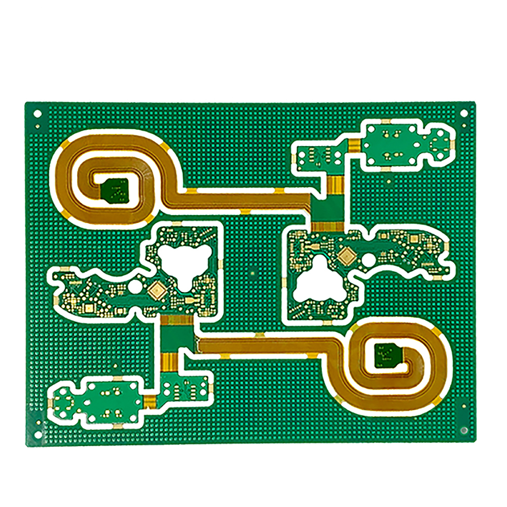
1-40 Layers Rigid Flex PCB
King Field is currently able to handle laminated multi-layer Rigid flex PCBs with up to 40 layers, and this is based on the premise that quality and delivery time can be guaranteed without mis-evaluation.Please tell us your length, size, number of layers, aperture, etc., and we will evaluate you immediately.
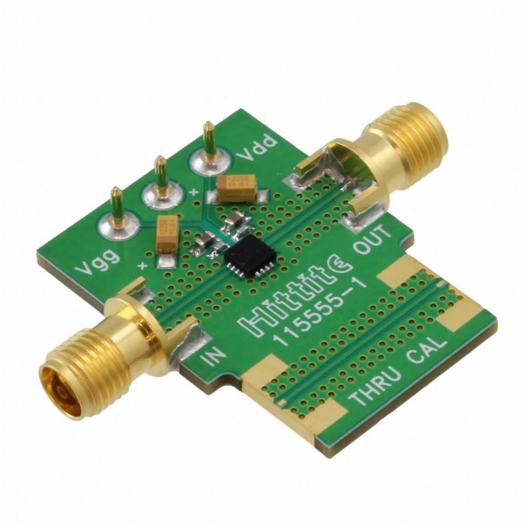
RF (Radio Frequency) PCB
RF PCBs are high-frequency PCBs with operating frequencies above 100MHz; anything above 2GHz is classified as a microwave PCB. The difficulty lies in the lamination process, and the layered structure is easily damaged during the perforation process. King Field has rich experience in solving these two problems and can provide you with the appropriate BOOM and GERBER file solutions.
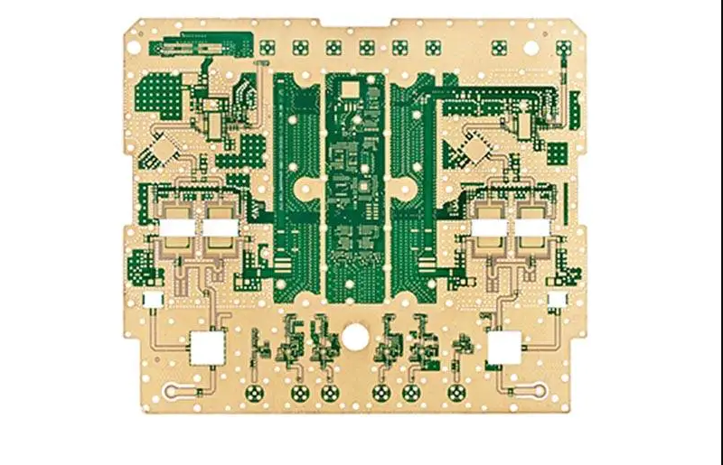
High Frequency PCB
Able to transmit high-frequency signals above 500MHz with minimal loss. Five significant advantages:
1. Reduce signal delay and improve frequency transmission.
2. Minimize signal loss and enhance signal transmission.
3. The size and shape of the PCB will not change with temperature changes, with super stability.
4. The PCB can withstand humid environments, waterproof and loss-resistant.
5. The generated material makes the PCB less prone to corrosion.
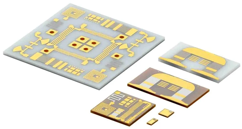
Ceramic PCB
Ceramic PCB has much better heat resistance and wear resistance than other types of PCB because of the layered structure materials including ceramics. Usually, it is subdivided into thick film ceramic PCB, thin film ceramic PCB, low temperature ceramic PCB, high temperature ceramic PCB, DPC ceramic PCBA, AMB ceramic PCB, etc. according to different processing technologies. King Field is the most outstanding supplier of ceramic PCB process capability solutions in China, and can solve problems that other factories cannot solve.
production capacity
| Items | Complex PCB |
| Material | PET/FR-4/Rogers/Ceramic/PCB Components/E-fibre glass/Arlon/Taconic |
| Layers | 1-40 Layers |
| Max cut lamination size | 500*420mm |
| Final board thickness | 0.20-6.0mm |
| Min Final Hole size | 0.075mm |
| Aspect Ratio | 14:01 |
| Inner layer Line Width/Space | 0.05mm |
| Copper Foil Thickness (Inner Layers) | 1/6oz-1oz |
| Min dielectric layer thickness | 20um |
| Copper Foil Thickness (Outer Layers) | 1/3oz-1oz |
| Copper to drill distance | 0.2mm |
| Out layer Line width/space | 0.035mm |
| Min SMD width | 0.05mm |
| Max Solder Mask Plug Hole Diameter | 0.5mm |
| solder mask strip width | 0.075mm |
| Final Set Size Tolerance | ±0.1mm/limit±0.05mm |
| Min Hole to board edge Distance | 0.075-0.15mm |
| Min Beveling angle Tolerance | ±3-5° |
| Layer to layer Tolerance | ≤0.075mm(1-6L) |
| Inner layer Min PTH Annular Ring | 0.15mm |
| Out layer Min PTH Annular ring | 0.15mm |
| Surface Treatment | OSP、HASL 、ENIG、Gold Finger、Plating Gold 、ENEPIG、IMM TIN、IMM AG |
| Warp&Twist | 0.5%(less than 45u) |
PCB factory display
Frequently Asked Questions
Our normal delivery time is very stable. If we encounter complex PCBs with special processes and performance, there will be a delay of 1-2 days.
No. We will provide a more cost-saving solution based on the existing BOOM. If you don’t have BOOM, you can enjoy King Field’s VIP service, a one-stop service to solve the “0-1” problem.
We provide design guidance, proofing, batch production, assembly, and material component purchasing services for complex PCBs. No matter which stage your project enters, we can provide you with effective solutions.
Of course. Compared to other companies, we follow up on business in shifts 24 hours a day, work 6 days a week, and the factory is open for manufacturing. This allows us to communicate more quickly and advance your project.
From the moment you send us your inquiry information via email, website form, online consultation, etc., we will provide you with PCB solutions for design, prototyping, manufacturing and assembly within one day at the earliest. All this is due to our integrated industry and trade company model and 20 years of industry experience.
Don't worry too much! Just provide as much existing information as possible, such as design or wiring files, material BOOM tables, generated GERBERs, performance parameter tables of finished products, etc.


